

Motorola MC1377P, MC1377DW Datasheet
Device
Operating
Temperature Range
Package
SEMICONDUCTOR
TECHNICAL DATA
COLOR TELEVISION
RGB to PAL/NTSC ENCODER
ORDERING INFORMATION
MC1377DW
MC1377P
TA = 0° to +70°C
SO–20L
Plastic DIP
Order this document by MC1377/D
P SUFFIX
PLASTIC PACKAGE
CASE 738
DW SUFFIX
PLASTIC PACKAGE
CASE 751D
(SO–20L)
20
1
20
1
1
MOTOROLA ANALOG IC DEVICE DATA
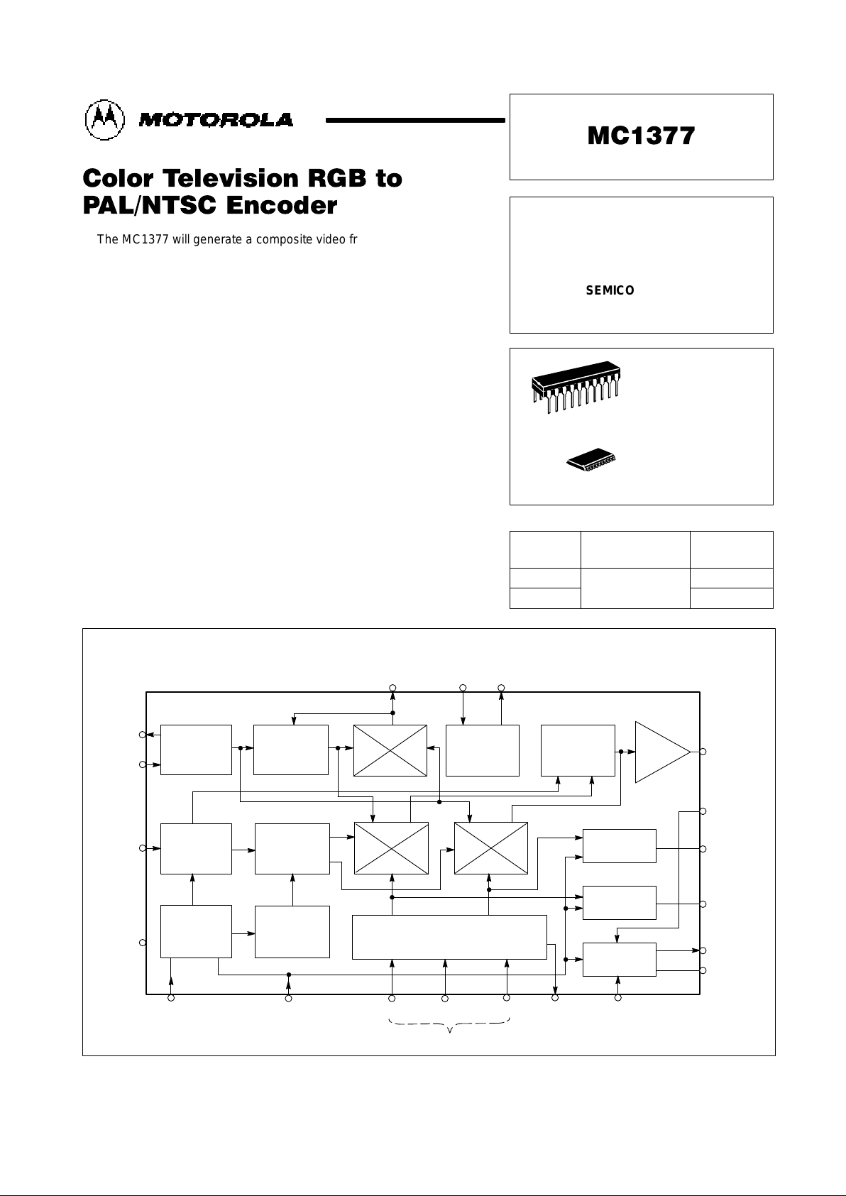
The MC1377 will generate a composite video from baseband red, green,
blue, and sync inputs. On board features include: a color subcarrier
oscillator; voltage controlled 90° phase shifter; two double sideband
suppressed carrier (DSBSC) chroma modulators; and RGB input matrices
with blanking level clamps. Such features permit system design with few
external components and accordingly, system performance comparable to
studio equipment with external components common in receiver systems.
• Self–contained or Externally Driven Reference Oscillator
• Chroma Axes, Nominally 90° (±5°), are Optionally Trimable
• PAL/NTSC Compatible
• Internal 8.2 V Regulator
Figure 1. Representative Block Diagram
Osc
out
Osc
in
NTSC/PAL
Select
Gnd
18
17
20
15
Quad
Decoup
V
CC
V
B
19 14 16
13
10
11
12
9
7
Chroma Out
Chroma In
B–Y Clamp
R–Y Clamp
Composite
Video Output
Video Clamp
1 2 3 4 5 6 8
T
rise
Composite
Sync Input
R G B
Inputs
–Y
out
–Y
in
Oscillator
Buffer
Voltage
Controlled
90
°
8.2V
Regulator
PAL
Switch
0/180
°
Chroma
Amp
B–Y
Clamp
R–Y
Clamp
Output Amp/
Clamp
Color Difference and
Luminance Matrix
Dual
Comparator
Latching
Ramp
Generator
PAL/NTSC
Control
Burst
Pulse
Driver
90
°
0
°
H/2
R–Y B–Y
R–Y B–Y
–Y
Motorola, Inc. 1995
MC1377
2
MOTOROLA ANALOG IC DEVICE DATA
MAXIMUM OPERATING CONDITIONS
Rating Symbol Value Unit
Supply Voltage V
CC
15 Vdc
Storage Temperature T
stg
–65 to +150 °C
Power Dissipation Package
Derate above 25°C
P
D
1.25
10
W
mW/°C
Operating Temperature T
A
0 to +70 °C
RECOMMENDED OPERATING CONDITIONS
Characteristics Min Typ Max Unit
Supply Voltage 10 12 14 Vdc
IB Current (Pin 16) 0 – –10 mA
Sync, Blanking Level (DC level between pulses, see Figure 9e)
Sync Tip Level (see Figure 9e)
Sync Pulse Width (see Figure 9e)
1.7
–0.5
2.5
–
0
–
8.2
0.9
5.2
Vdc
µ
s
R, G, B Input (Amplitude)
R, G, B Peak Levels for DC Coupled Inputs, with Respect to Ground
–
2.2
1.0
–
–
4.4
V
pp
V
Chrominance Bandwidth (Non–comb Filtered Applications), (6 dB) 0.5 1.5 2.0 MHz
Ext. Subscarrier Input (to Pin 17) if On–Chip Oscillator is not used. 0.5 0.7 1.0 V
pp
ELECTRICAL CHARACTERISTICS (V
CC
= 12 Vdc, TA = 25°C, circuit of Figure 7, unless otherwise noted.)
Characteristics
Pins Symbol Min Typ Max Unit
SUPPLY CURRENT
Supply Current into V
CC,
No Load, on Pin 9. VCC = 10 V
Circuit Figure 7 VCC = 11 V
VCC = 12 V
VCC = 13 V
VCC = 14 V
14 I
CC
–
–
20
–
–
33
34
35
36
37
–
–
40
–
–
mA
VOLTAGE REGULATOR
VB Voltage (IB = –10 mA, VCC = 12 V, Figure 7)
Load Regulation (0 < IB ≤ 10 mA, VCC = 12 V)
Line Regulation (IB = 0 mA, 10 V < VCC < 14 V) ≤
16 V
B
Reg
load
Reg
line
7.7
–20
–
8.2
120
4.5
8.7
+30
–
Vdc
mV
mV/V
OSCILLATOR AND MODULATION
Oscillator Amplitude with 3.58 MHz/4.43 MHz crystal 17 Osc – 0.6 – V
pp
Subcarrier Input: Resistance at 3.58 MHz
Subcarrier Input: Resistance at 4.43 MHz
17 R
osc
–
–
5.0
4.0
–
–
kΩ
Capacitance C
osc
– 2.0 – pF
Modulation Angle (R–Y) to (B–Y)
Angle Adjustment (R–Y)
DC Bias Voltage
–
19
19
∅m
∆∅m
V
19
–
–
–
±5
0.25
6.4
–
–
–
Deg
Deg/µA
Vdc
CHROMINANCE AND LUMINANCE
Chroma Input DC Level
Chroma Input Level for 100% Saturation
10 V
in
–
–
4.0
0.7
–
–
Vdc
V
pp
Chroma Input: Resistance
Chroma Input: Capacitance
R
in
C
in
–
–
10
2.0
–
–
kΩ
pF
Chroma DC Output Level
Chroma Output Level at 100% Saturation
13 V
out
8.9
–
10
1.0
10.9
–
Vdc
V
pp
Chroma Output Resistance R
out
– 50 –
Ω
Luminance Bandwidth (–3.0 dB), Less Delay Line 9 BW
Luma
– 8.0 – MHz
MC1377
3
MOTOROLA ANALOG IC DEVICE DATA
ELECTRICAL CHARACTERISTICS (V
CC
= 12 Vdc, TA = 25°C, circuit of Figure 7, unless otherwise noted.)
Characteristics
Pins Symbol Min Typ Max Unit
VIDEO INPUT
R, G, B Input DC Levels 3, 4, 5 RGB 2.8 3.3 3.8 Vdc
R, G, B Input for 100% Color Saturation – 1.0 – V
pp
R, G, B Input: Resistance
R, G, B Input: Capacitance
R
RGB
C
RGB
8.0
–
10
2.0
17
–
k
Ω
pF
Sync Input Resistance (1.7 V < Input < 8.2) 2
Sync
– 10 –
k
Ω
COMPOSITE VIDEO OUTPUT
Composite Output,
100% Saturation
(see Figure 8d)
Sync
Luminance
Chroma
Burst
9 CV
out
–
–
–
–
0.6
1.4
1.7
0.6
–
–
–
–
V
pp
Output Impedance (Note 1) R
video
– 50 –
Ω
Subcarrier Leakage in Output (Note 2) V
lk
– 20 – mV
pp
NOTES: 1. Output Impedance can be reduced to less than 10 Ω by using a 150 Ω output load from Pin 9 to ground. Power supply current will
increase to about 60 mA.
2.Subcarrier leakage can be reduced to less than 10 mV with optional circuitry (see Figure 12).
PIN FUNCTION DESCRIPTIONS
Symbol Pin Description
t
r
1 External components at this pin set the rise time of the internal ramp function generator (see Figure 10).
Sync
2 Composite sync input. Presents 10 kΩ resistance to input.
R 3 Red signal input. Presents 10 kΩ impedance to input. 1.0 Vpp required for 100% saturation.
G 4 Green signal input. Presents 10 kΩ impedance to input. 1.0 Vpp
required for 100% saturation.
B 5 Blue signal Input. Presents 10 kΩ impedance to input. 1.0 Vpp
required for 100% saturation.
–Y
out
6 Luma (–Y) output. Allows external setting of luma delay time.
V
clamp
7 Video Clamp pin. Typical connection is a 0.01 µF capacitor to ground.
–Y
in
8 Luma (–Y) input. Presents 10 kΩ input impedance.
CV
out
9 Composite Video output. 50 Ω output impedance.
Chroma
In
10 Chroma input. Presents 10 kΩ input impedance.
B–Y
clamp
11 B–Y clamp. Clamps B–Y during blanking with a 0.1 µF capacitor to ground.
Also used with R–Y clamp to null residual color subcarrier in output.
R–Y
clamp
12 R–Y clamp. Clamps R–Y during blanking with a 0.1 µF capacitor to ground.
Also used with B–Y clamp to null residual color subcarrier in output.
Chroma
Out
13 Chroma output. 50 Ω output impedance.
V
CC
14 Power supply pin for the IC; +12, ± 2.0 V, required at 35 mA (typical).
Gnd 15 Ground pin.
V
B
16 8.2 V reference from an internal regulator capable of delivering 10 mA to external circuitry.
Osc
in
17 Oscillator input. A transistor base presents 5.0 kΩ to an external subcarrier input, or is available for
constructing a Colpitts oscillator (see Figure 4).
Osc
out
18 Oscillator output. The emitter of the transistor, with base access at Pin 17, is accessible for completing the
Colpitts oscillator. See Figure 4.
∅
m
19 Quad decoupler. With external circuitry, R–Y to B–Y relative angle errors can be corrected. Typically,
requires a 0.01 µF capacitor to ground.
NTSC/PAL
Select
20 NTSC/PAL switch. When grounded, the MC1377 is in the NTSC mode; if unconnected, in the PAL mode.
MC1377
4
MOTOROLA ANALOG IC DEVICE DATA
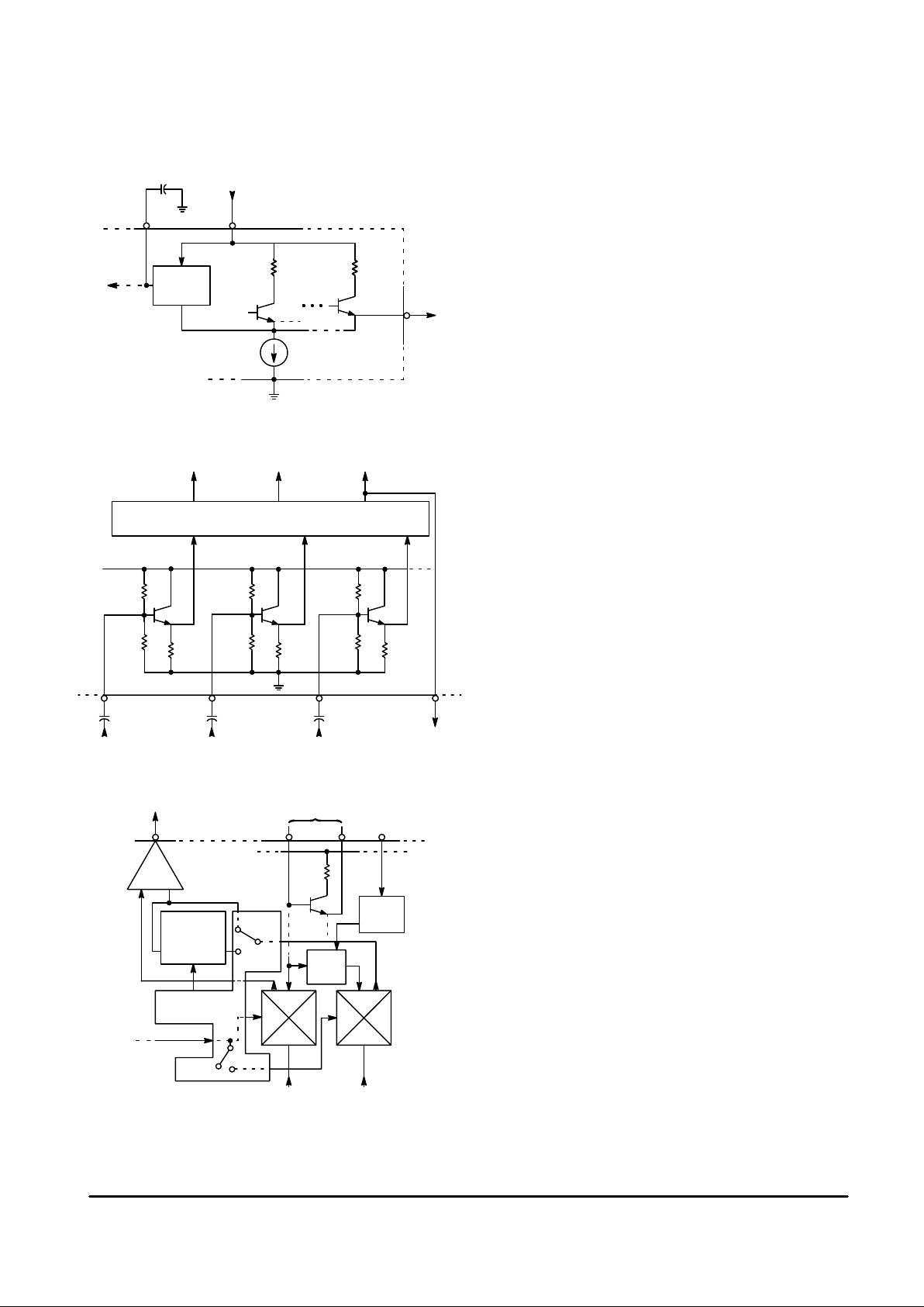
FUNCTIONAL DESCRIPTION
Figure 2. Power Supply and V
B
0.1
VCC = +12V
16
14
15
32mA
8.2V
Regulator
9
100
Figure 3. RGB Input Circuitry
13 17 18 19
Chroma
Out
Oscillator
Quad
Decoup
Amp/
Buffer
∆ Θ
PAL
Switch
0/180
°
NTSC
PAL
PAL/NTSC
Control
Burst
Flag
NTSC
PAL
B–Y R–Y
B–Y R–Y
+90
°
R
Figure 4. Chroma Section
R–Y
15µF
3
18k
B–Y –Y
RGB Matrix
18k
18k
15µF
4
G
15µF
5
B
6
–Y
27k 27k
27k
Power Supply and VB (8.2 V Regulator)
The MC1377 pin for power supply connection is Pin 14.
From the supply voltage applied to this pin, the IC biases
internal output stages and is used to power the 8.2 V internal
regulator (VB at Pin 16) which biases the majority of internal
circuitry. The regulator will provide a nominal 8.2 V and is
capable of 10 mA before degradation of performance. An
equivalent circuit of the supply and regulator is shown in
Figure 2.
R, G, B Inputs
The RGB inputs are internally biased to 3.3 V and provide
10 k
Ω of input impedance. Figure 3 shows representative
input circuitry at Pins 3, 4, and 5.
The input coupling capacitors of 15 µF are used to prevent
tilt during the 50/60 Hz vertical period. However, if it is desired
to avoid the use of the capacitors, then inputs to Pins 3, 4,
and 5 can be dc coupled provided that the signal levels are
always between 2.2 V and 4.4 V.
After input, the separate RGB information is introduced to
the matrix circuitry which outputs the R–Y, B–Y, and –Y
signals. The –Y information is routed out at Pin 6 to an
external delay line (typically 400 ns).
DSBSC Modulators and 3.58 MHz Oscillator
The R–Y and B–Y outputs (see (B–Y)/(R–Y) Axes versus
I/Q Axes, Figure 22) from the matrix circuitry are amplitude
modulated onto the 3.58/4.43 MHz subcarrier. These signals
are added and color burst is included to produce composite
chroma available at Pin 13. These functions plus others,
depending on whether NTSC or P AL operation is chosen, are
performed in the chroma section. Figure 4 shows a block
diagram of the chroma section.
The MC1377 has two double balanced mixers, and
regardless of which mode is chosen (NTSC or PAL), the
mixers always perform the same operation. The B–Y mixer
modulates the color subcarrier directly, the R–Y mixer
receives a 90
° phase shifted color subcarrier before being
modulated by the R–Y baseband information. Additional
operations are then performed on these two signals to make
them NTSC or PAL compatible.
In the NTSC mode, the NTSC/PAL control circuitry allows
an inverted burst of 3.58 MHz to be added only to the B–Y
signal. A gating pulse or “burst flag” from the timing section
permits color burst to be added to the B–Y signal. This color
burst is 180° from the B–Y signal and 90° away from the R–Y
signal (see Figure 22) and permits decoding of the color
information. These signals are then added and amplified
before being output, at Pin 13, to be bandpassed and then
reintroduced to the IC at Pin 10.
In the PAL mode, NTSC/PAL control circuitry allows an
inverted 4.43 MHz burst to be added to both R–Y and B–Y
equally to produce the characteristic PAL 225°/135 burst
phase. Also, the R–Y information is switched alternately from
180° to 0° of its original position and added to the B–Y
information to be amplified and output.
MC1377
5
MOTOROLA ANALOG IC DEVICE DATA
Timing Circuitry
The composite sync input at Pin 2 performs three
important functions: it provides the timing (but not the
amplitude) for the sync in the final output; it drives the black
level clamps in the modulators and output amplifier; and it
triggers the ramp generator at Pin 1, which produces burst
envelope and P AL switching. A representative block diagram
of the timing circuitry is shown in Figure 5.
In order to produce a color burst, a burst envelope must be
generated which “gates” a color subcarrier into the R–Y and
B–Y modulators. This is done with the ramp generator at
Pin 1.
The ramp generator at Pin 1 is an R–C type in which the
pin is held low until the arrival of the
leading
edge of sync. The
rising ramp function, with time constant R–C, passes through
two level sensors – the first one starts the gating pulse and
the second stops it (see Figure 10). Since the “early” part of
the exponential is used, the timing provided is relatively
accurate from chip–to–chip and assembly–to–assembly.
Fixed components are usually adequate. The ramp
continues to rise for more than half of the line interval, thereby
inhibiting burst generation on “half interval” pulses on vertical
front and back porches. The ramp method will produce burst
on the vertical front and back “porches” at full line intervals.
R–Y, B–Y Clamps and Output Clamp/Amplifier
The sync signal, shown in the block diagram of Figure 6,
drives the R–Y and B–Y clamps which clamp the R–Y and
B–Y signals to reference black during the blanking periods.
The output amplifier/clamp provides this same function plus
combines and amplifies the chroma and luma components
for composite video output.
Application Circuit
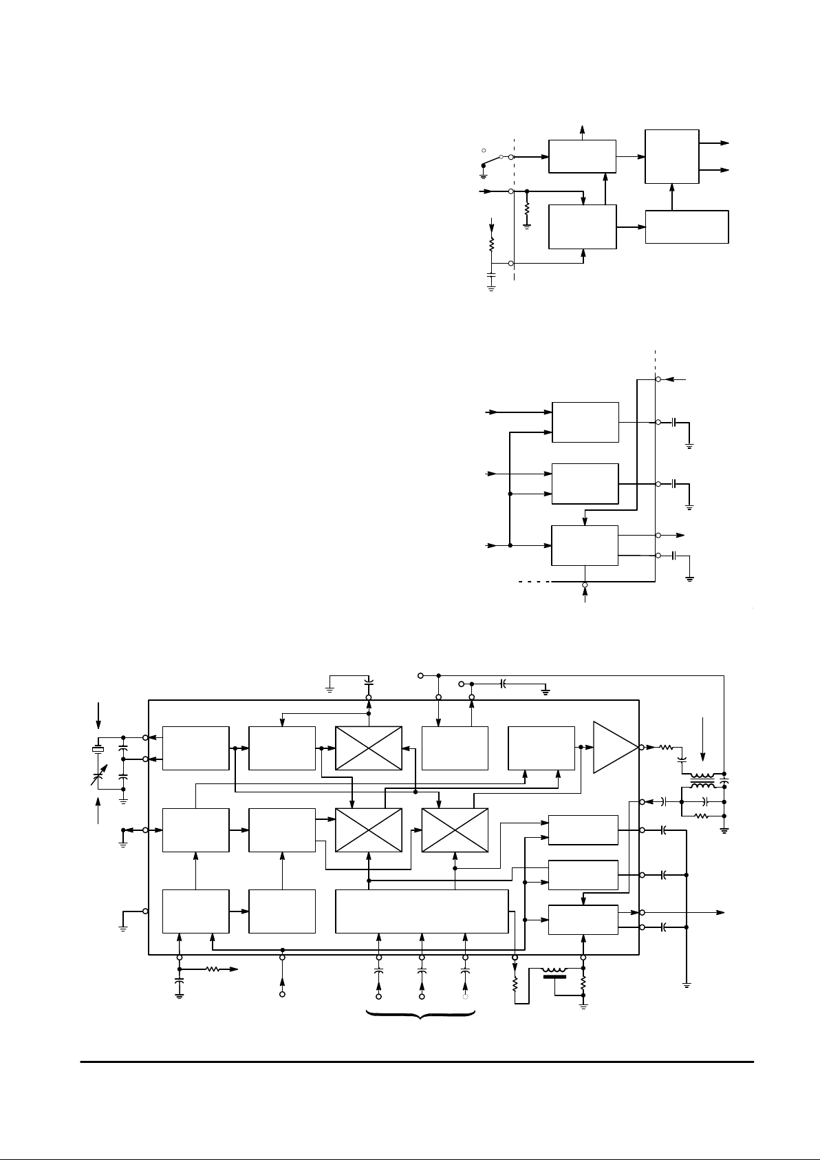
Figure 7 illustrates the block diagram of the MC1377 and
the external circuitry required for typical operation.
11
Sync
Input
Figure 5. Timing Circuitry
Figure 6. R–Y, B–Y and Output Amplifier Clamps
PAL/
NTSC
H/2
Line Drive
10k
Latching
Ramp
Generator
Dual
Comparator
Burst Flag
Burst
Pulse
Driver
PAL/NTSC
Control
20
2
1
B–Y
R–Y
Sync
B–Y
Clamp
R–Y
Clamp
Output
Amp/Clamp
Chroma
10
12
9
7
8
–Y
Composite
Video
V
B
R
C
0.1
0.1
0.01
Figure 7. Block Diagram and Application Circuit
R–Y B–Y
Osc/
Buffer
Voltage
Controlled
90
°
8.2V
Regulator
PAL
Switch
0/180
°
Chroma
Amp
B–Y
Clamp
R–Y
Clamp
Output Amp/
Clamp
Color Difference and
Luminance Matrix
Dual
Comparator
Latching
Ramp
Gen
PAL/NTS
C
Control
Burst
Pulse
Driver
0.01
19
V
CC
16
V
B
0.1
TOKO 166NNF
–10264AG
13
220
100/
62*
0.1
3.3k
47/33*
10
9
7
0.01
12
0.1
0.1
1000
3.58/
4.43*
MHz
220
220
5.0 to
25pF
20
15
1 2
3
4 5 6
8
56k
0.001
mica
Composite
Sync
Input
14
11
Composite
Video Output
1.0k
400ns
Y Delay
1.0k
+ + +
15
µ
F 15µF 15µF
V
B
R G B
R, G, B Inputs
H/2
90
°
0
°
NTSC/
PAL Select
17
18
* Refers to the choice NTSC/PAL
* (3.58 MHz/4.43 MHz).
R–Y
B–Y
–Y
–Y

MC1377
6
MOTOROLA ANALOG IC DEVICE DATA
10k
R29
R21
220
R161
15k
R127
27k
R129
18k
R126
2.7k
R123
3.9k
T111
T23
22k
R28
R4
2.0k
+12V
+8.2V
Gnd
PAL/NTSC
Comp Sync
T
RISE
R–IN
G–IN
B–IN
R6A 5.1k
Z1
R2
1.2k
R2A
1.0k
T1
R3
6.8k
R13
22k
R11
22k
R12
10k
R14
22k
R22
270
R9
22k
560
R25
560
R26
T22
T19 T20
R23
1.5k
R24
1.5k
R18
220
R20
220
T17
T15
T16
T24 T25 T26 T27
T10
T13
R16
1.0k
R17
1.0k
T9
T8T7
R8
220
R9
220
R5
470
T5T4
+
C1
5pF
R6
5.1k
R10
5.0k
R15
T2 T3
R7
4.0k
+
C2
18pF
T11 T12
T28
5.0k
R30
R162
R71
22k
R69
R70
10k
R72
22k
R73
22k
R74
10k
R75
10k
T79
T68
T69
R77
15k
R76
15k
R80A
4.0k
R81
22k
T71
T73
T74
R83
10k
R79
1.0k
R78
15k
Z2
T75
R86
10k
T76
R87
13.8k
R88
30.4k
T77
R95
18k
T82
T81
R94
2.2k
R93
2.2k
R92
2.2k
R91
10k
T78
T79
T80
R85
10k
T72
R82
22k
R100
22k
T91B
T91A
R96
22k
R101
10k
R97
22k
R102
1.0k
T90
R99
10k
R98
22k
T92 T93
T94
R160
22k
R104
2.0k
R104
15k
R108
2.7k
R164
4.7k
T102
T103
T104
T101T100
T99T98
R107
820
T95
R105
7.5k
R110
1.0k
T105
R111
4.7k
T107
R112
36k
R113
27k
R118
R117
10k
R120
27k
T110
T109
T108
R115
18k
R119
5.3k
R116
3.9k
R122
18k
T96
R106
9.1k
R109
22k
T206
T97
191817
14
16
15
20
2
1
3
4
5
Osc In Osc Out
Quad
Decoup
10k
R121
27k
22k
R90
R80 B
6.0k
T18
T6
T14
1.5k
220
R27
220
22k
10k
 Loading...