

Motorola MC1350P, MC1350D Datasheet
The MC1350 is an integrated circuit featuring wide range AGC for use as
an IF amplifier in radio and TV over an operating temperature range of 0° to
+75°C.
• Power Gain: 50 dB Typ at 45 MHZ
Power Gain: 50 dB Typ at 58 MHZ
• AGC Range: 60 dB Min, DC to 45 MHz
• Nearly Constant Input & Output Admittance over the Entire AGC Range
•
Constant ( –3.0 dB) to 90 MHz
Y21
• Low Reverse Transfer Admittance: < < 1.0 µmho Typ
• 12 V Operation, Single–Polarity Power Supply
MAXIMUM RATINGS
Power Supply Voltage V
Output Supply Voltage V1, V
AGC Supply Voltage V
Differential Input Voltage V
Power Dissipation (Package Limitation)
Plastic Package
Derate above
Operating Temperature Range T
(TA = +25°C, unless otherwise noted.)
Rating
25°C
Symbol Value Unit
+
AGC
in
P
D
A
8
+18 Vdc
+18 Vdc
+
V
5.0 Vdc
625
5.0
0 to +75 °C
Vdc
mW
mW/°C
IF AMPLIFIER
SEMICONDUCTOR
TECHNICAL DATA
8
1
D SUFFIX
PLASTIC PACKAGE
CASE 751
(SO–8)
ORDERING INFORMATION
Device
MC1350P
MC1350D
Temperature Range
Order this document by MC1350/D
P SUFFIX
PLASTIC PACKAGE
CASE 626
8
1
Operating
TA = 0° to +75°C
Package
Plastic DIP
SO–8
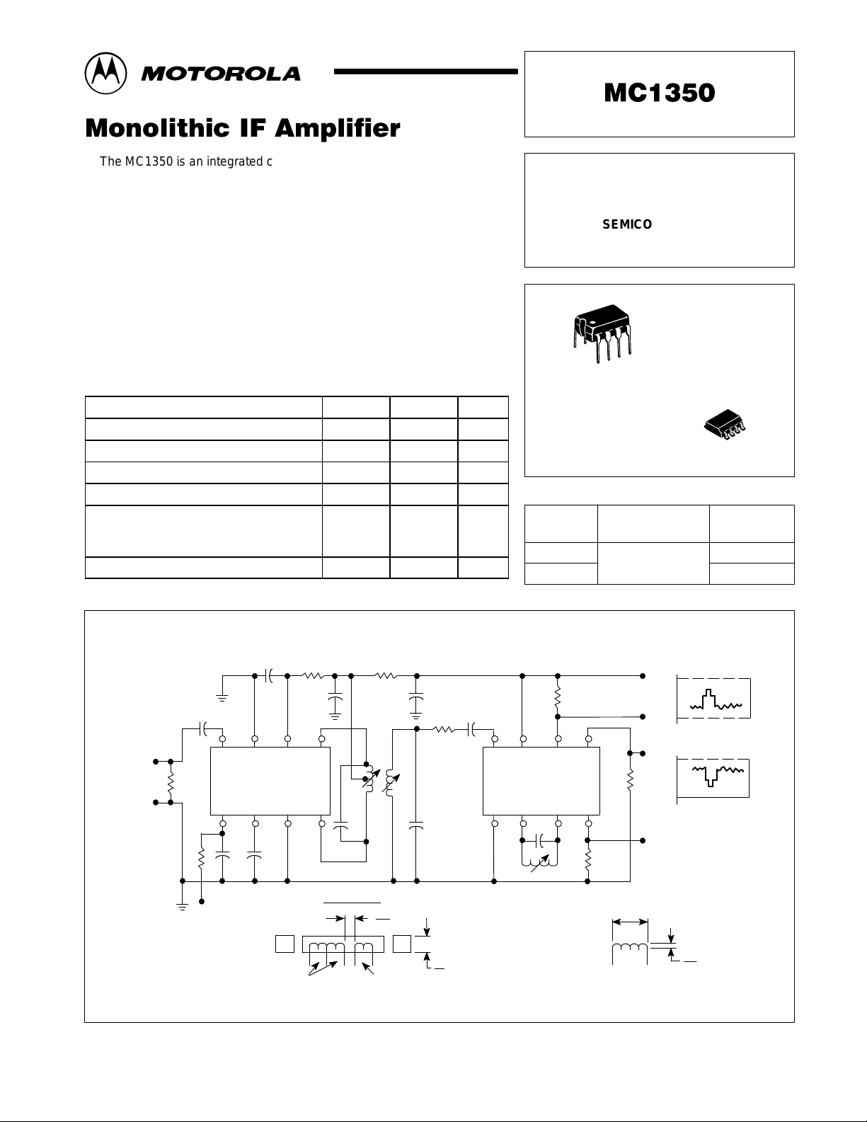
Figure 1. T ypical MC1350 Video IF Amplifier and MC1330 Low–Level Video Detector Circuit
45MHz
Input
0.001µF
4
50
567
5.0k
AGC
0.002µF
321
MC1350
F
µ
0.002
470 220
0.1
µ
22
12pF
1
″
4
F
µ
F
0.002
T1
8
F
µ
0.002
5
Turns
All windings #30 AWG tinned nylon acetate
wire tuned with Carbonyl E or J slugs.
T1
20pF
5
″
≈
16
Turns
6
3.3k
68pF
76 5 4
MC1330AP
83 2 1
33pF
L1
L1 wound with #26 AWG tinned nylon
acetate wire tuned by distorting winding.
+18Vdc
Auxiliary Video
Output
3.9k
3
″
16
10
Turns
18V
10V
Primary Video
and Sound Output
7.7V
3.9k
0
AFT Output
3
16
″
MOTOROLA ANALOG IC DEVICE DATA
Motorola, Inc. 1996 Rev 3
1
MC1350
ELECTRICAL CHARACTERISTICS
Characteristics
AGC Range, 45 MHz (5.0 V to 7.0 V) (Figure 1) 60 68 – dB
Power Gain (Pin 5 grounded via a 5.1 kΩ resistor)
f = 58 MHz, BW = 4.5 MHz See Figure 6(a)
f = 45 MHz, BW = 4.5 MHz See Figure 6(a), (b)
f = 10.7 MHz, BW = 350 kHz See Figure 7
f = 455 kHz, BW = 20 kHz
Maximum Differential Voltage Swing
0 dB AGC
–30 dB AGC
Output Stage Current (Pins 1 and 8) I1 + I
Total Supply Current (Pins 1, 2 and 8) I
Power Dissipation P
DESIGN PARAMETERS, Typical Values (V
Parameter Symbol 455 kHz 10.7 MHz 45 MHz 58 MHz Unit
Single–Ended Input Admittance g
Input Admittance Variations with AGC
(0 dB to 60 dB)
Differential Output Admittance g
Output Admittance Variations with AGC
(0 dB to 60 dB)
Reverse Transfer Admittance (Magnitude) |y12| < < 1.0 < < 1.0 < < 1.0 < < 1.0 µmho
Forward Transfer Admittance
Magnitude
Angle (0 dB AGC)
Angle (–30 dB AGC)
Single–Ended Input Capacitance C
Differential Output Capacitance C
(V+ = +12 Vdc, TA = +25°C, unless otherwise noted.)
Symbol Min Typ Max Unit
A
p
V
O
8
S
D
+
= +12 Vdc, TA = +25°C, unless otherwise noted.)
11
b
11
∆g
∆b
22
b
22
∆g
∆b
|y21|
< y
< y
11
11
22
22
21
21
in
O
0.31
0.022
–
–
4.0
3.0
–
–
160
–5.0
–3.0
7.2 7.2 7.4 7.6 pF
1.2 1.2 1.3 1.6 pF
–
46
–
–
–
–
– 5.6 – mA
– 14 17 mAdc
– 168 204 mW
Frequency
0.36
0.50
–
–
4.4
110
–
–
160
–20
–18
0.39
2.30
60
0
30
390
4.0
90
200
–80
–69
48
50
58
62
20
8.0
–
–
–
–
–
–
0.5
2.75
–
–
60
510
–
–
180
–105
–90
mmho
µmho
µmho
µmho
mmho
Degrees
Degrees
dB
V
pp
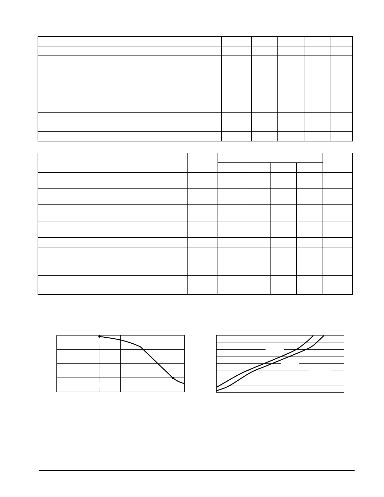
Figure 2. T ypical Gain Reduction Figure 3. Noise Figure versus Gain Reduction
0
I
= 0.1 mA
20
40
60
GAIN REDUCTION (dB)
80
4.0 5.0 6.0 7.0
AGC
(Figures 6 and 7)
V
, SUPPLY VOLTAGE (V)
AGC
I
AGC
= 0.2 mA
2
22
20
18
16
14
12
10
NOISE FIGURE (dB)
8.0
6.0
0 10203040
58 MHz
45 MHz
(Figure 6)
GAIN REDUCTION (dB)
MOTOROLA ANALOG IC DEVICE DATA
 Loading...