

Motorola MC13282AP Datasheet
Device
Operating
Temperature Range
Package
SEMICONDUCTOR
TECHNICAL DATA
100 MHz VIDEO PROCESSOR
WITH OSD INTERFACE
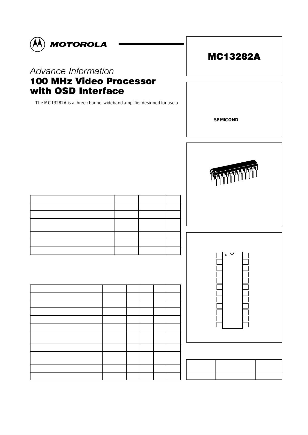
ORDERING INFORMATION
MC13282AP TA = 0° to +70°C Plastic DIP
P SUFFIX
PLASTIC PACKAGE
CASE 724
24
1
Order this document by MC13282A/D
PIN CONNECTIONS
124
23
22
21
20
19
18
17
2
3
4
5
6
7
8
(Top View)
R Subcontrast
R Input
G Subcontrast
B Input
Gnd
R
OSD
Blank
Video V
CC
16
15
14
13
9
10
11
12
G
OSD
OSD Contrast
B
OSD
Contrast
G Input
B Subcontrast
V
CC
Clamp
R Emitter
R Clamp
V5
G Emitter
G Clamp
Fast Commutate
B Clamp
B Emitter
NDIP–24
1
MOTOROLA ANALOG IC DEVICE DATA
The MC13282A is a three channel wideband amplifier designed for use as
a video pre–amp in high resolution RGB color monitors.
Features:
• 4.0 Vpp Output with 100 MHz Bandwidth
• 3.5 ns Rise/Fall Time
• Subcontrast Control for Each Channel
• Blanking and Clamping Inputs
• Contrast Control
• OSD Interface with 50 MHz Bandwidth
• OSD Contrast Control
• Package: NDIP–24
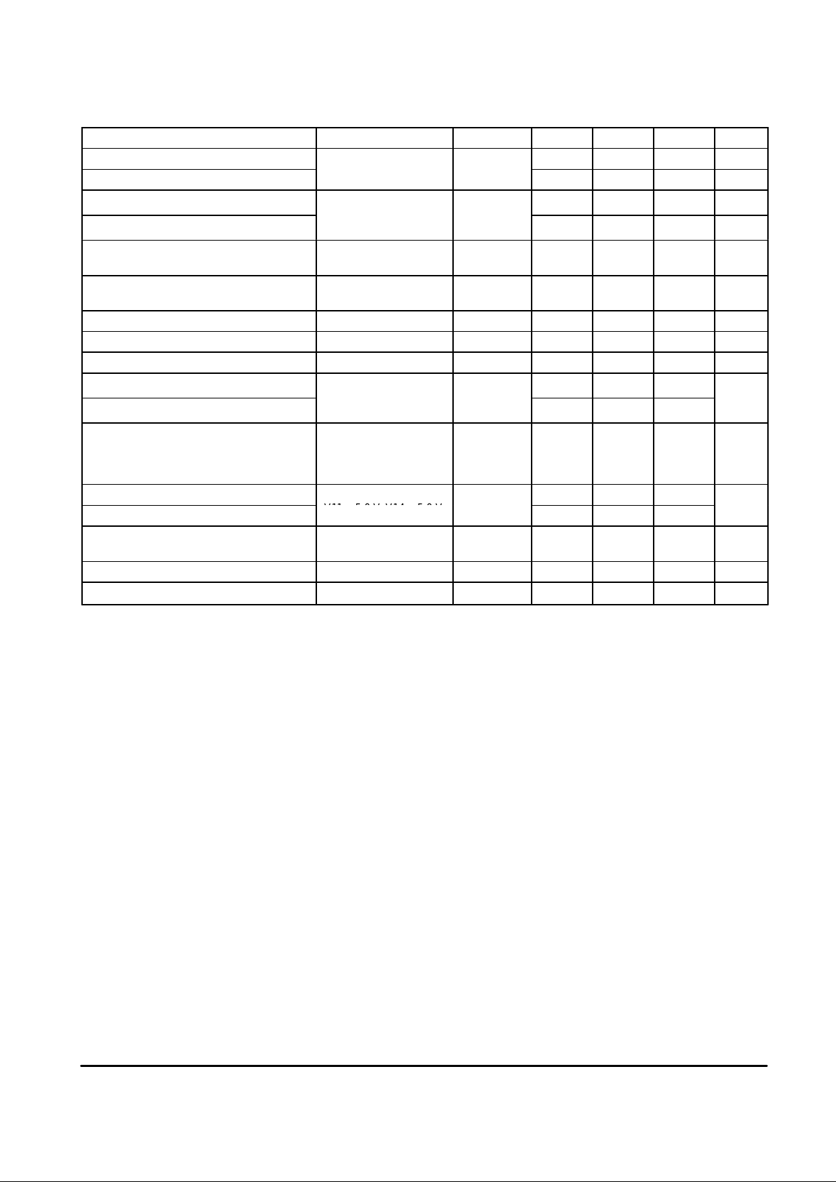
ABSOLUTE MAXIMUM RATINGS
Rating Pin Value Unit
Power Supply Voltage – V
CC
9 –0.5, 10 Vdc
Power Supply Voltage – Video V
CC
17 –0.5, 10 Vdc
Voltage at Video Amplifier Inputs 2, 4, 6, 8,
10, 12
–0.5, +5.0 Vdc
Collector–Emitter Current (Three Channels) 17 120 mA
Storage Temperature – –65 to +150 °C
Junction Temperature – 150 °C
NOTES: 1.Devices should not be operated at these limits. Refer to “Recommended
Operating Conditions” section for actual device operation.
2.ESD data available upon request.
RECOMMENDED OPERATING CONDITIONS
Characteristic Pin Min Typ Max Unit
Power Supply Voltage 9, 17 7.6 8.0 8.4 Vdc
Contrast Control 13 0 – 5.0 Vdc
Subcontrast Control 1, 3, 5 0 – 5.0 Vdc
Blanking Input Signal Amplitude 24 0 – 5.0 V
Clamping Input Signal Amplitude 23 0 – 5.0 V
Video Signal Amplitude
(with 75 Ω Termination)
2, 4, 6 – 0.7 1.0 Vpp
OSD Signal Input 8, 10, 12 – TTL – V
Collector–Emitter Current
(Total for Three Channels)
17 0 – 50 mA
Clamping Pulse Width 23 500 – – ns
Operating Ambient Temperature – 0 – 70 °C
This document contains information on a new product. Specifications and information herein
are subject to change without notice.
Motorola, Inc. 1996 Rev 0
MC13282A
2
MOTOROLA ANALOG IC DEVICE DATA
ELECTRICAL CHARACTERISTICS
(Refer to Test Circuit Figure 1, TA = 25°C, VCC = 8.0 Vdc.)
Characteristic
Condition Pin Min Typ Max Unit
Input Impedance
– 2, 4, 6
100 – – kΩ
Internal DC Bias Voltage
– 2.4 – Vdc
Output Signal Amplitude
V2, V4, V6 = 0.7 Vpp
15, 19, 22
3.6 4.0 – Vpp
Voltage Gain
V1, V3, V5, V13
= 5.0
V
V14 = 0 V
– 5.6 – V/V
Contrast Control V13 = 5.0 to 0 V
V1, V3, V5 = 5.0 V
13 – –26 – dB
Subcontrast Control V1, V3, V5 = 5.0 to 0 V
V13 = 5.0 V
1, 3, 5 – –26 – dB
Emitter DC Level – 15, 19, 22 1.0 1.2 1.4 Vdc
Blanking Input Threshold – 24 – 1.25 – V
Clamping Input Threshold – 23 – 3.75 – V
Video Rise Time
V2, V4, V6 = 0.7 Vpp
15, 19, 22
– 3.5 –
ns
Video Fall Time
V
out
=
4.0 V
pp
RL > 300 Ω, CL < 5.0 pF
– 3.5 –
Video Bandwidth V2, V4, V6 = 0.7 Vpp
V1, V3, V5, V13 = 5.0 V
V14 = 0 V
RL > 300 Ω, CL < 5.0 pF
15, 19, 22 – 100 – MHz
OSD Rise Time
V8, V10, V12 = TTL Level
15, 19, 22
– 7.0 –
ns
OSD Fall Time
V11 = 5.0 V, V14 = 5.0 V
– 7.0 –
OSD Bandwidth V8, V10, V12 = TTL Level
V11 = 5.0 V, V14 = 5.0 V
15, 19, 22 – 50 – MHz
OSD Propagation Delay – – – 17 – ns
Power Supply Current VCC, Video VCC = 8.0 V 9, 17 – 70 – mA
NOTE: It is recommended to use a double sided PCB layout for high frequency measurement (e.g., rise/fall time, bandwidth).
MC13282A
3
MOTOROLA ANALOG IC DEVICE DATA
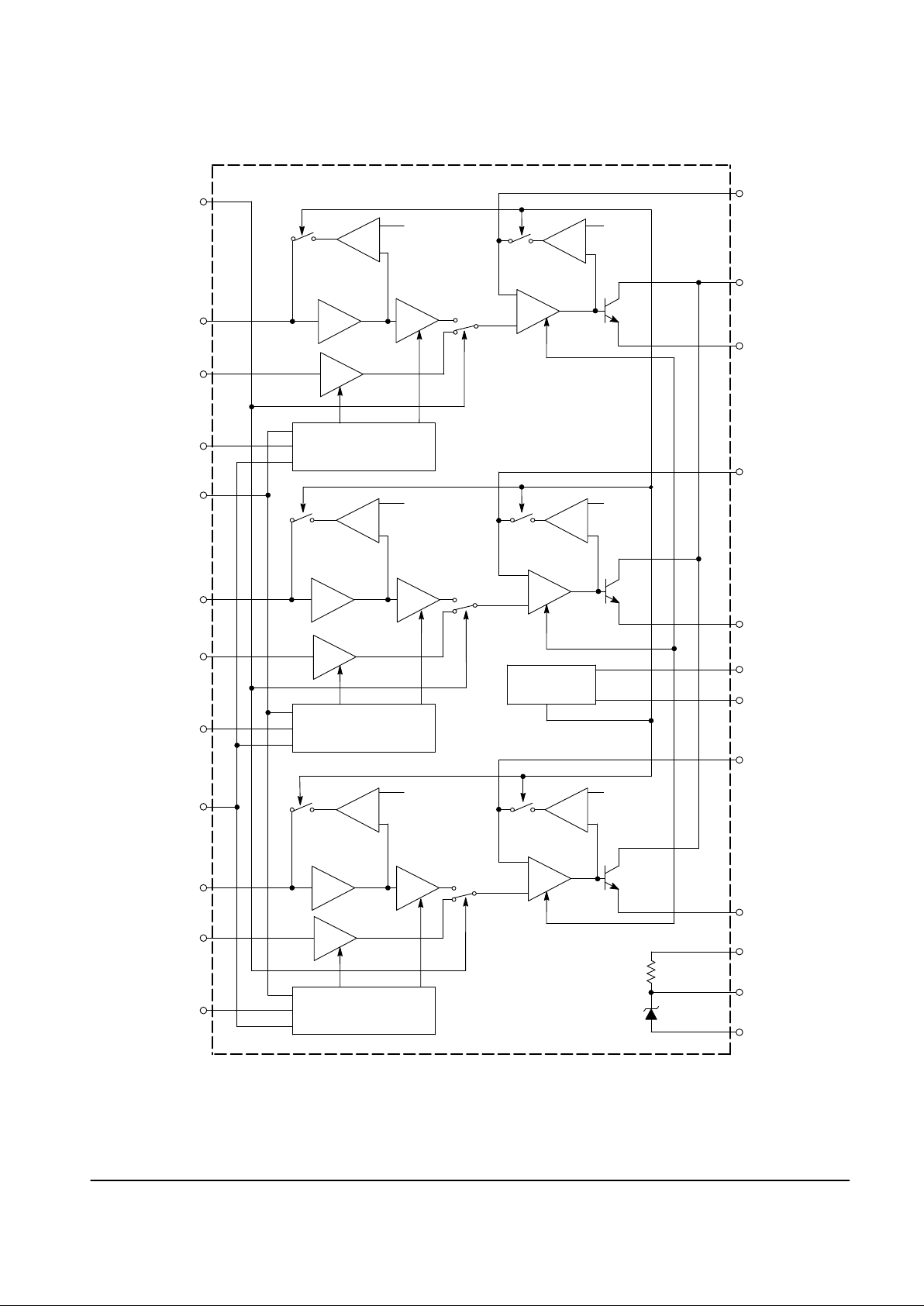
Figure 1. Internal Block Diagram
2
Fast Commutate
14
R Input
R
OSD
R Subcontrast
Contrast
G Input
G
OSD
G Subcontrast
OSD Contrast
B Input
B
OSD
B Subcontrast
R Clamp
Video V
CC
R Emitter
G Clamp
G Emitter
Blank
Clamp
B Clamp
B Emitter
V
CC
V5
Gnd
V
ref1
V
ref1
V
ref1
V
ref2
V
ref2
V
ref2
R Channel
G Channel
B Channel
Clamp Blank
Decoder
Contrast and Subcontrast
Control Processor
Contrast and Subcontrast
Control Processor
Contrast and Subcontrast
Control Processor
8
1
13
4
10
3
11
6
12
5
21
17
22
18
19
24
23
16
15
9
20
7
This device contains 272 active transistors.
MC13282A
4
MOTOROLA ANALOG IC DEVICE DATA
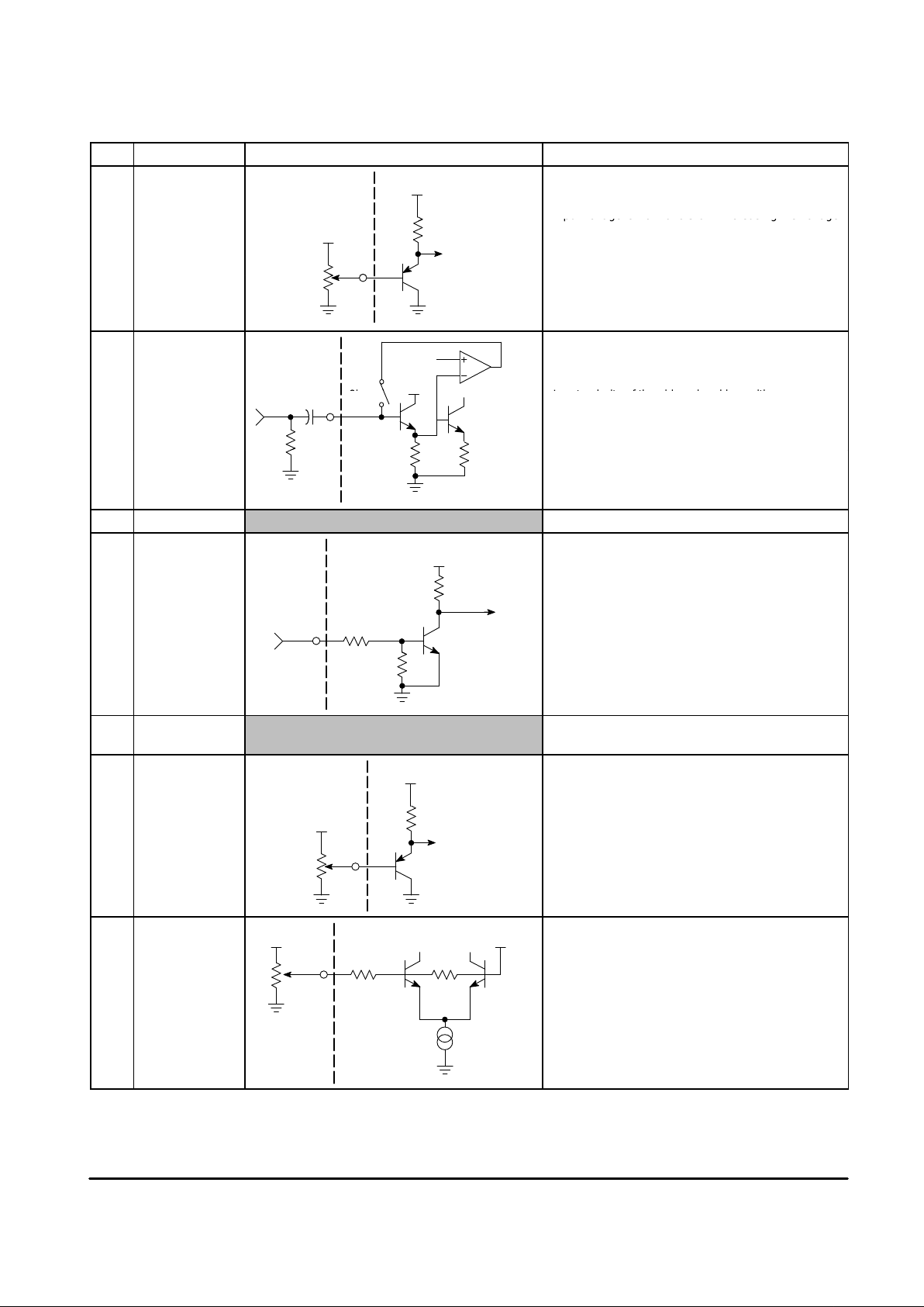
PIN FUNCTION DESCRIPTION
Pin Name Equivalent Internal Circuit Description
1 R Subcontrast
Control
V
CC
These pin provides a maximum of 26 dB attenuation
to vary the gain of each video amplifier separately.
Input voltage is from 0 to 5.0 V . Increasing the voltage
3 G Subcontrast
Control
5.0 V
50 k
Input voltage is from 0 to 5.0 V. Increasing the voltage
will increase the contrast level.
5 B Subcontrast
Control
2 R Input
5.0 V
V
ref
The input coupling capacitor is used for input
clamping storage. The maximum source impedance
is 100 Ω.
4 G Input
5.0 V
Clamp
75
Ω
0.1
Input polarity of the video signal is positive.
Nominal 0.7 Vpp input signal is recommended
(maximum 1.0 Vpp).
6 B Input
1.0 k10 k
75
Ω
7 Ground Ground pin. Connect to a clean, solid ground.
8 R
OSD
Input
V
CC
These inputs are standard TTL level.
10 G
OSD
Input
80 k
12 B
OSD
Input
60 k
9 V
CC
Connect to 8.0 Vdc supply, ±5%. Decoupling is
required at this pin.
11 OSD Contrast
5.0 V
V
CC
3.5 k
On Screen Display contrast control.
Input voltage is from 0 to 5.0 V . Increasing the voltage
will increase the contrast of the OSD signal.
13 Contrast
2.5 V
42 k
5.0 V
2.0 k
Overall Contrast Control for the three channels.
The input range is 0 V to 5.0 V . An increase of voltage
increases the contrast.
 Loading...