

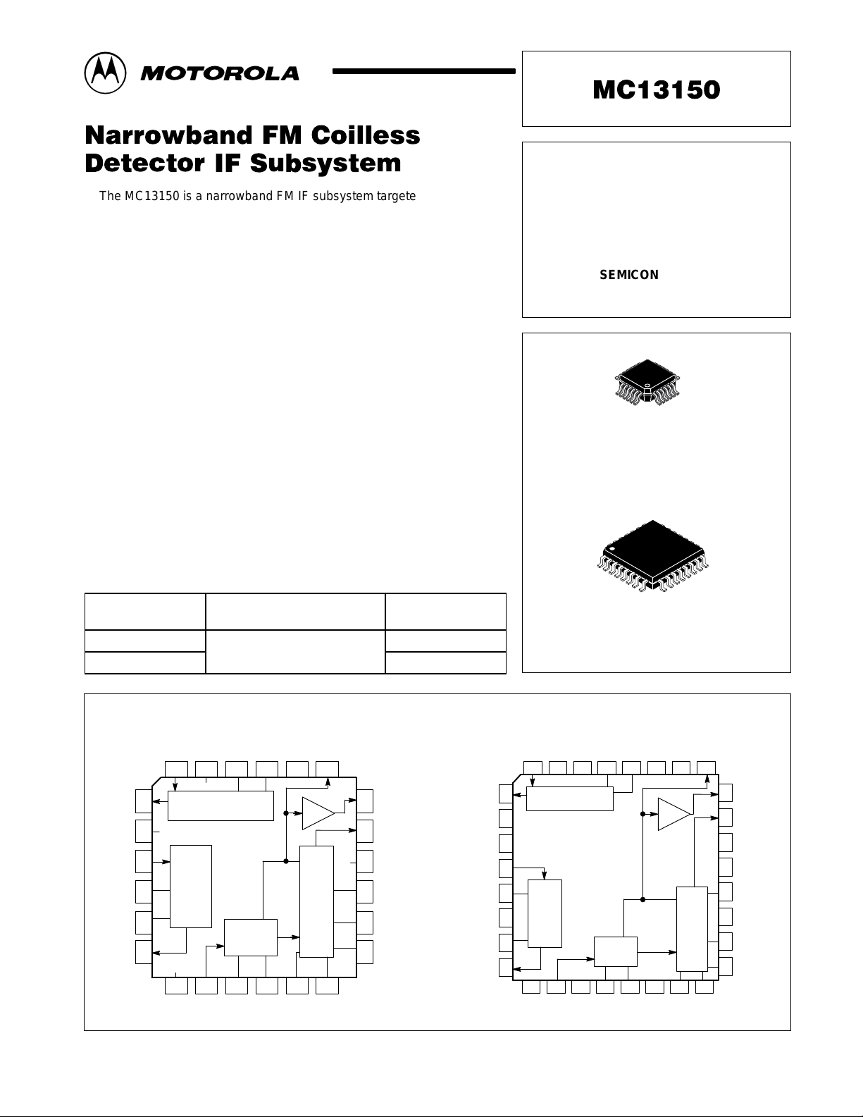
Motorola MC13150FTB, MC13150FTA Datasheet
T
85°C
Order this document by MC13150/D
The MC13150 is a narrowband FM IF subsystem targeted at cellular and
other analog applications. Excellent high frequency performance is
achieved, with low cost, through use of Motorola’s MOSAIC 1.5 RF bipolar
process. The MC13150 has an onboard Colpitts VCO for Crystal controlled
second LO in dual conversion receivers. The mixer is a double balanced
configuration with excellent third order intercept. It is useful to beyond
200 MHz. The IF amplifier is split to accommodate two low cost cascaded
filters. RSSI output is derived by summing the output of both IF sections. The
quadrature detector is a unique design eliminating the conventional tunable
quadrature coil.
Applications for the MC13150 include cellular, CT–1 900 MHz cordless
telephone, data links and other radio systems utilizing narrowband FM
modulation.
• Linear Coilless Detector
• Adjustable Demodulator Bandwidth
• 2.5 to 6.0 Vdc Operation
• Low Drain Current: <2.0 mA
• Typical Sensitivity of 2.0 µV for 12 dB SINAD
• IIP3, Input Third Order Intercept Point of 0 dBm
• RSSI Range of Greater Than 100 dB
• Internal 1.4 kΩ Terminations for 455 kHz Filters
• Split IF for Improved Filtering and Extended RSSI Range
ORDERING INFORMATION
Operating
Device
MC13150FT A
MC13150FTB
Temperature Range
–
°
= –40 ° to +
A
°
Package
LQFP–24
LQFP–32
NARROWBAND FM COILLESS
DETECTOR IF SUBSYSTEM
FOR CELLULAR AND
ANALOG APPLICATIONS
SEMICONDUCTOR
TECHNICAL DATA
24 1
FTA SUFFIX
PLASTIC PACKAGE
CASE 977
(LQFP–24)
32
1
FTB SUFFIX
PLASTIC PACKAGE
CASE 873
(LQFP–32)
LQFP–24 LQFP–32
PIN CONNECTIONS
Mix
V
out
CC1
IF
IF
IF
IF
out
d1
d2
in
EE1
V
Mix
24 23 22 21 20 19
1
2
3
in
4
5
6
Mixer
IF
789101112
in
CC2
LIM
V
LOeLO
Limiter
LIMd1LIM
d2
b
Enable
RSSI
Detector
AdjFAdj
BW
18
17
16
15
14
13
RSSI
DET
V
EE2
DET
AFT
AFT
b
out
Gain
Filt
out
Mix
Out
V
CC1
VCC (N/C)
IF
in
IF
d1
VCC (N/C)
IF
d2
IF
out
MOTOROLA ANALOG IC DEVICE DATA
in
Mix
32 31 28 27 26 2530 29
1
2
3
4
5
IF
6
7
8
910 1314151611 12
CC2
V
Motorola, Inc. 1997 Rev 2
EE1
V
Mixer
in
LIM
V
V
CC
CC
(N/C)
(N/C)
LOeLO
Limiter
LIMd1LIM
d2
b
CC
V
Enable
V
CC
(N/C)
(N/C)
Detector
AdjFAdj
BW
RSSI
24
23
22
21
20
19
18
17
RSSI
DET
VEE (N/C)
V
DET
VEE (N/C)
AFT
AFT
b
out
EE2
Gain
Filt
out
1
MC13150
Á
Á
Á
Á
Á
Á
Á
Á
ÁÁÁÁ
Á
Á
Á
Á
Á
Á
ÁÁÁÁ
Á
Á
Á
Á
Á
ÁÁÁÁ
Á
Á
Á
Á
Á
ÁÁÁÁ
Á
Á
Á
Á
Á
ÁÁÁÁ
Á
Á
Á
Á
Á
Á
Á
Á
Á
Á
Á
Á
Á
Á
Á
Á
Á
Á
Á
Á
Á
Á
Á
Á
Á
Á
Á
Á
Á
Á
Á
Á
Á
Á
Á
Á
Á
Á
Á
Á
Á
Á
Á
Á
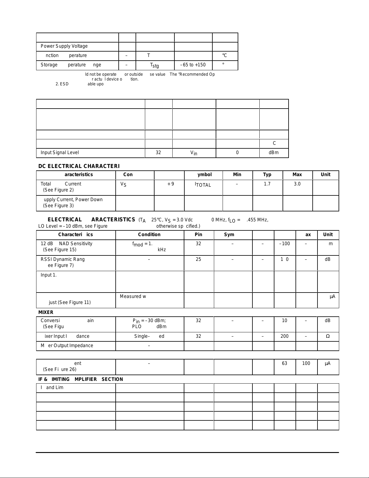
MAXIMUM RATINGS
Rating Pin Symbol Value Unit
Power Supply Voltage
Junction Temperature
Storage Temperature Range
NOTE: 1. Devices should not be operated at or outside these values. The ”Recommended Operating
Limits” provide for actual device operation.
2.ESD data available upon request.
RECOMMENDED OPERATING CONDITIONS
Rating Pin Symbol Value Unit
Power Supply Voltage TA = 25°C
БББББББББББ
(See Figure 22)
БББББББББББ
Input Frequency
БББББББББББ
Ambient Temperature Range
БББББББББББ
Input Signal Level
БББББББББББ
–40°C ≤ TA ≤ 85°C
2, 9
–
–
VCC(max)
T
Jmax
T
stg
2, 9
21, 31
ÁÁ
ÁÁ
32
ÁÁ
–
ÁÁ
32
ÁÁ
6.5
+150
–65 to +150
V
CC
V
ÁÁÁÁ
EE
ÁÁÁÁ
f
in
ÁÁÁÁ
T
A
ÁÁÁÁ
V
in
ÁÁÁÁ
Vdc
°C
°C
2.5 to 6.0
0
ÁÁÁÁ
ÁÁÁÁ
10 to 500
ÁÁÁÁ
–40 to +85
ÁÁÁÁ
0
ÁÁÁÁ
Vdc
ÁÁÁ
ÁÁÁ
MHz
ÁÁÁ
°C
ÁÁÁ
dBm
ÁÁÁ
DC ELECTRICAL CHARACTERISTICS (T
Characteristics
Total Drain Current
(See Figure 2)
ББББББББ
Supply Current, Power Down
Condition Pin Symbol Min Typ Max Unit
VS = 3.0 Vdc
ÁÁÁ
–
= 25°C, V
A
ÁÁ
CC1
2 + 9
2 + 9
= V
CC2
ÁÁÁÁ
(See Figure 3)
AC ELECTRICAL CHARACTERISTICS (T
= 25°C, VS = 3.0 Vdc, fRF = 50 MHz, fLO = 50.455 MHz,
A
LO Level = –10 dBm, see Figure 1 Test Circuit*, unless otherwise specified.)
Characteristics
12 dB SINAD Sensitivity
ББББББББ
(See Figure 15)
RSSI Dynamic Range
(See Figure 7)
ББББББББ
Input 1.0 dB Compression Point
Input 3rd Order Intercept Point
ББББББББ
(See Figure 18)
Coilless Detector Bandwidth
Adjust (See Figure 11)
ББББББББ
Condition Pin Symbol Min Typ Max Unit
f
= 1.0 kHz;
mod
ББББББ
f
= ±5.0 kHz
dev
ÁÁÁ
–
ББББББ
ÁÁÁ
–
ББББББ
–
ÁÁÁ
Measured with No IF Filters
ББББББ
ÁÁÁ
MIXER
Conversion Voltage Gain
(See Figure 5)
Mixer Input Impedance
Mixer Output Impedance
Pin = –30 dBm;
PLO = –10 dBm
Single–Ended
–
LOCAL OSCILLATOR
LO Emitter Current
ББББББББ
(See Figure 26)
ББББББ
–
ÁÁÁ
IF & LIMITING AMPLIFIERS SECTION
IF and Limiter RSSI Slope
IF Gain
IF Input & Output Impedance
Limiter Input Impedance
Limiter Gain
* Figure 1 Test Circuit uses positive (VCC) Ground.
Figure 7
Figure 8
–
–
–
= 3.0 Vdc, No Input Signal.)
I
TOTAL
–
32
25
–
–
–
32
32
1
29
25
4, 8
4, 8
10
–
–
ÁÁÁ
–
–
ÁÁÁ
–
ÁÁÁ
1.0 dB C. Pt.
IIP3
ÁÁÁ
∆BW adj
ÁÁÁ
–
–
–
–
ÁÁÁ
–
–
–
–
–
1.7
ÁÁ
40
–
Á
–
Á
–
–
Á
–
Á
–
–
–
30
Á
–
–
–
–
–
–100
Á
100
Á
–11
–1.0
Á
26
Á
10
200
1.5
63
Á
0.4
42
1.5
1.5
96
3.0
ÁÁ
–
ÁÁ
ÁÁ
ÁÁ
ÁÁ
ÁÁ
–
–
–
–
–
–
–
–
100
–
–
–
–
–
mA
ÁÁ
nA
dBm
Á
dB
Á
dBm
Á
kHz/µA
Á
dB
Ω
kΩ
µA
Á
µA/dB
dB
kΩ
kΩ
dB
2
MOTOROLA ANALOG IC DEVICE DATA
MC13150
AC ELECTRICAL CHARACTERISTICS (continued) (T
LO Level = –10 dBm, see Figure 1 Test Circuit*, unless otherwise specified.)
Characteristics UnitMaxTypMinSymbolPinCondition
DETECTOR
Frequency Adjust Current Figure 9,
Frequency Adjust Voltage Figure 10,
Bandwidth Adjust Voltage Figure 12,
Detector DC Output Voltage
(See Figure 25)
Recovered Audio Voltage f
* Figure 1 Test Circuit uses positive (VCC) Ground.
fIF = 455 kHz
fIF = 455 kHz
I15 = 1.0 µA
– 23 – – 1.36 – Vdc
= ±3.0 kHz 23 – 85 122 175 mVrms
dev
= 25°C, VS = 3.0 Vdc, fRF = 50 MHz, fLO = 50.455 MHz,
A
Figure 1. T est Circuit
LO Input
Local
Oscillator
Limiter
Mixer
In
IF
In
49.9
IF Amp
Out
Mixer
Out
220 n
220 n
10
1:4
Z Xformer
220 n
1.5 k
220 n
220 n
220 n
1.5 k
µ
+
V
EE1
220 n
100 n
31 30 29 28 27 26 25
32
V
EE1
1
2
3
4
5
6
7
8
Mixer
V
CC1
IF
V
CC2
910111213141516
16 – 41 49 56 µA
16 – 600 650 700 mVdc
15 – – 570 – mVdc
100 n
Enable
49.9
RSSI
Buffer
V
(6)
Detector
EE2
24
23
22
21
20
19
18
17
100 p
100 k
RSSI
Buffer
V18–V17 = 0;
fIF = 455 kHz
RSSI
Detector
Output
R
L
100 k
R
S
100 k
220 n 10
+
V
EE2
µ
Limiter
In
MOTOROLA ANALOG IC DEVICE DATA
220 n
49.9
This device contains 292 active transistors.
220 n
220 n
220 n
I16I15
3

MC13150
MC13150 CIRCUIT DESCRIPTION
General
The MC13150 is a very low power single conversion
narrowband FM receiver incorporating a split IF. This device
is designated for use as the backend in analog narrowband
FM systems such as cellular, 900 MHz cordless phones and
narrowband data links with data rates up to 9.6 k baud. It
contains a mixer, oscillator, extended range received signal
strength indicator (RSSI), RSSI buffer , IF amplifier , limiting IF,
a unique coilless quadrature detector and a device enable
function (see Package Pin Outs/Block Diagram).
Low Current Operation
The MC13150 is designed for battery and portable
applications. Supply current is typically 1.7 mAdc at 3.0 Vdc.
Figure 2 shows the supply current versus supply voltage.
Enable
The enable function is provided for battery powered
operation. The enabled pin is pulled down to enable the
regulators. Figure 3 shows the supply current versus enable
voltage, V
device. Note that the device is fully enabled at VCC – 1.3 Vdc.
Figure 4 shows the relationship of enable current, I
enable voltage, V
Mixer
The mixer is a double–balanced four quadrant multiplier
and is designed to work up to 500 MHz. It has a single ended
input. Figure 5 shows the mixer gain and saturated output
response as a function of input signal drive and for –10 dBm
LO drive level. This is measured in the application circuit
shown in Figure 15 in which a single LC matching network is
used. Since the single–ended input impedance of the mixer is
200 Ω, an alternate solution uses a 1:4 impedance
transformer to match the mixer to 50 Ω input impedance. The
linear voltage gain of the mixer alone is approximately 4.0 dB
(plus an additional 6.0 dB for the transformer). Figure 6
shows the mixer gain versus the LO input level for various
mixer input levels at 50 MHz RF input.
(relative to VCC) needed to enable the
enable
.
enable
enable
to
The buffered output of the mixer is internally loaded,
resulting in an output impedance of 1.5 kΩ.
Local Oscillator
The on–chip transistor operates with crystal and LC
resonant elements up to 220 MHz. Series resonant, overtone
crystals are used to achieve excellent local oscillator stability .
3rd overtone crystals are used through about 65 to 70 MHz.
Operation from 70 MHz up to 200 MHz is feasible using the
on–chip transistor with a 5th or 7th overtone crystal. To
enhance operation using an overtone crystal, the internal
transistor’s bias is increased by adding an external resistor
from Pin 29 (in 32 pin QFP package) to VEE to keep the
oscillator on continuously or it may be taken to the enable pin
to shut it off when the receiver is disabled. –10 dBm of local
oscillator drive is needed to adequately drive the mixer
(Figure 6). The oscillator configurations specified above are
described in the application section.
RSSI
The received signal strength indicator (RSSI) output is a
current proportional to the log of the received signal
amplitude. The RSSI current output is derived by summing
the currents from the IF and limiting amplifier stages. An
external resistor at Pin 25 (in 32 pin QFP package) sets the
voltage range or swing of the RSSI output voltage. Linearity
of the RSSI is optimized by using external ceramic bandpass
filters which have an insertion loss of 4.0 dB. The RSSI circuit
is designed to provide 100+ dB of dynamic range with
temperature compensation (see Figures 7 and 23 which
show the RSSI response of the applications circuit).
RSSI Buffer
The RSSI buffer has limitations in what loads it can drive.
It can pull loads well towards the positive and negative
supplies, but has problems pulling the load away from the
supplies. The load should be biased at half supply to
overcome this limitation.
4
MOTOROLA ANALOG IC DEVICE DATA
MC13150
Figure 2. Supply Current
versus Supply V oltage
2.0
1.6
1.2
0.8
, SUPPLY CURRENT (mA)
0.4
SUPPLY
I
0
1.5 2.5 3.5 4.5 5.5 6.5 7.5
V
, SUPPLY VOLTAGE (Vdc)
ENABLE
TA = 25°C
Figure 4. Enable Current
versus Enable V oltage
70
60
µ
50
40
30
20
, ENABLE CURRENT (
10
0
ENABLE
IA)
–10
0 0.4 0.8 1.2 1.6 2.0
V
, ENABLE VOLTAGE (Vdc)
ENABLE
VCC = 3.0 Vdc
TA = 25
Figure 3. Supply Current
versus Enable V oltage
°
C
Measured
CC
0.7 0.9 1.1 1.3 1.5
V
, ENABLE VOLTAGE (Vdc)
ENABLE
, SUPPLY CURRENT (A)
SUPPLY
I
10
10
10
10
10
10
10
10
10
–2
–3
–4
–5
–6
–7
–8
–9
–10
VCC = 3.0 Vdc
TA = 25
V
ENABLE
Relative to V
0.5
Figure 5. Mixer IF Output Level versus
RF Input Level
20
VEE = –3.0 Vdc
°
C
10
0
–10
–20
–30
MIXER IF OUTPUT LEVEL (dBm)
–40
–50
–50 –40 –30 –20 –10 0
TA = 25
°
C
fRF = 50 MHz; fLO = 50.455 MHz
LO Input Level = –10 dBm
(100 mVrms)
(Rin = 50
RF INPUT LEVEL (dBm)
Ω
; R
= 1.4 k
out
Ω
10 20
Figure 6. Mixer IF Output Level versus
Local Oscillator Input Level
20
VEE = –3.0 Vdc
°
C
TA = 25
0
–20
–40
–60
MIXER IF OUTPUT LEVEL (dBm)
–80
–60 –50 –40 –30 –20 –10 0
fRF = 50 MHz; fLO = 50.455 MHz
Ω
Rin = 50
LO DRIVE (dBm)
; R
out
= 1.4 k
RF In = 0 dBm
MOTOROLA ANALOG IC DEVICE DATA
–20 dBm
–40 dBm
Ω
Figure 7. RSSI Output Current
versus Input Signal Level
50
VCC = 3.0 Vdc
f = 50 MHz
40
µ
RSSI OUTPUT CURRENT ( A)
fLO = 50.455 MHz
455 kHz
Ceramic Filter
30
See Figure 15
20
10
0
–120 –100 –80 –60 –40 –20 0
SIGNAL INPUT LEVEL (dBm)
5
MC13150
j
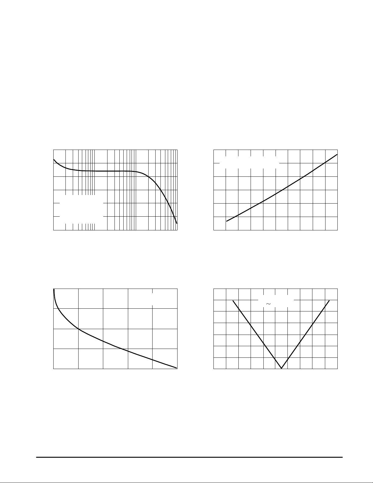
IF Amplifier
The first IF amplifier section is composed of three
differential stages. This section has internal dc feedback and
external input decoupling for improved symmetry and
stability. The total gain of the IF amplifier block is
approximately 42 dB at 455 kHz. Figure 8 shows the gain of
the IF amplifier as a function of the IF frequency .
The fixed internal input impedance is 1.5 kΩ; it is designed
for applications where a 455 kHz ceramic filter is used and no
external output matching is necessary since the filter requires
a 1.5 kΩ source and load impedance.
Figure 8. IF Amplifier Gain
versus IF Frequency
50
45
40
35
Vin = 100 µV
30
IF AMP GAIN (dB)
25
20
0.01 0.1 1.0 10
Ω
Rin = 50
R
= 1.4 k
out
BW (3.0 dB) = 2.4 MHz
TA = 25
Ω
°
C
f, FREQUENCY (MHz)
Overall RSSI linearity is dependent on having total
midband attenuation of 10 dB (4.0 dB insertion loss plus 6.0
dB impedance matching loss) for the filter. The output of the
IF amplifier is buffered and the impedance is 1.5 kΩ.
Limiter
The limiter section is similar to the IF amplifier section
except that six stages are used. The fixed internal input
impedance is 1.5 kΩ. The total gain of the limiting amplifier
section is approximately 96 dB. This IF limiting amplifier
section internally drives the quadrature detector section.
Figure 9. F
Current
adj
versus IF Frequency
120
VCC = 3.0 Vdc
100
Slope at 455 kHz = 9.26 kHz/
µ
80
60
CURRENT (
40
adj
FA)
20
0
0
200 400 600 800 1000
µ
A
f, IF FREQUENCY (kHz)
Figure 10. F
versus F
800
750
700
VOLTAGE (mVdc)
adj
F
650
600
0 20 40 60 80 100
F
CURRENT (µA)
ad
adj
Current
adj
Voltage
VCC = 3.0 Vdc
TA = 25
Figure 11. BW
Current
adj
versus IF Frequency
3.5
°
C
3.0
2.5
µ
2.0
1.5
CURRENT (
adj
1.0
BW A)
0.5
0
400 420 440 460 480 500
VCC = 3.0 Vdc
26 kHz/µA
BW
f, IF FREQUENCY (kHz)
6
MOTOROLA ANALOG IC DEVICE DATA
 Loading...