

Motorola MC13144D Datasheet
# "
"!
The MC13144 is designed in the Motorola High Frequency Bipolar
MOSIAC V wafer process to provide excellent performance in analog and
digital communication systems. It includes a cascoded LNA usable up to
2.0 GHz and at 1.8 Vdc, with 2 bit digital programming of the LNA bias.
Targeted applications are in the UHF Family Radio Services, UHF and
800 MHz Special Mobile Radio, 800 MHz Cellular and GSM, PCS, DECT
and PHS at 1.8 to 2.0 GHz and Cordless Telephones in the 902 to 928 MHz
band covered by FCC Title 47; Part 15. The MC13144 offers the following
features:
• 17 dB Gain at 900 MHz
• 1.4 dB Noise Figure at 900 MHz
• 1.0 dB Compression Point of –7.0 dBm; Input Third Order Intercept
Point of –5.0 dBm
• Low Operating Supply Voltage (1.8 to 6.0 Vdc)
• Programmable Bias with Enable 1 and Enable 2
• Enable 1 and Enable 2 Programmed High for Optimal Noise Figure and
Gain Associated with NF
• Can Override Enable and Externally Program In Up to 15 mA
Order this document by MC13144/D
VHF – 2.0 GHz LOW
NOISE AMPLIFIER WITH
PROGRAMMABLE BIAS
SEMICONDUCTOR
TECHNICAL DATA
8
1
D SUFFIX
PLASTIC PACKAGE
CASE 751
(SO–8)
MOSAIC V is a trademark of Motorola, Inc.
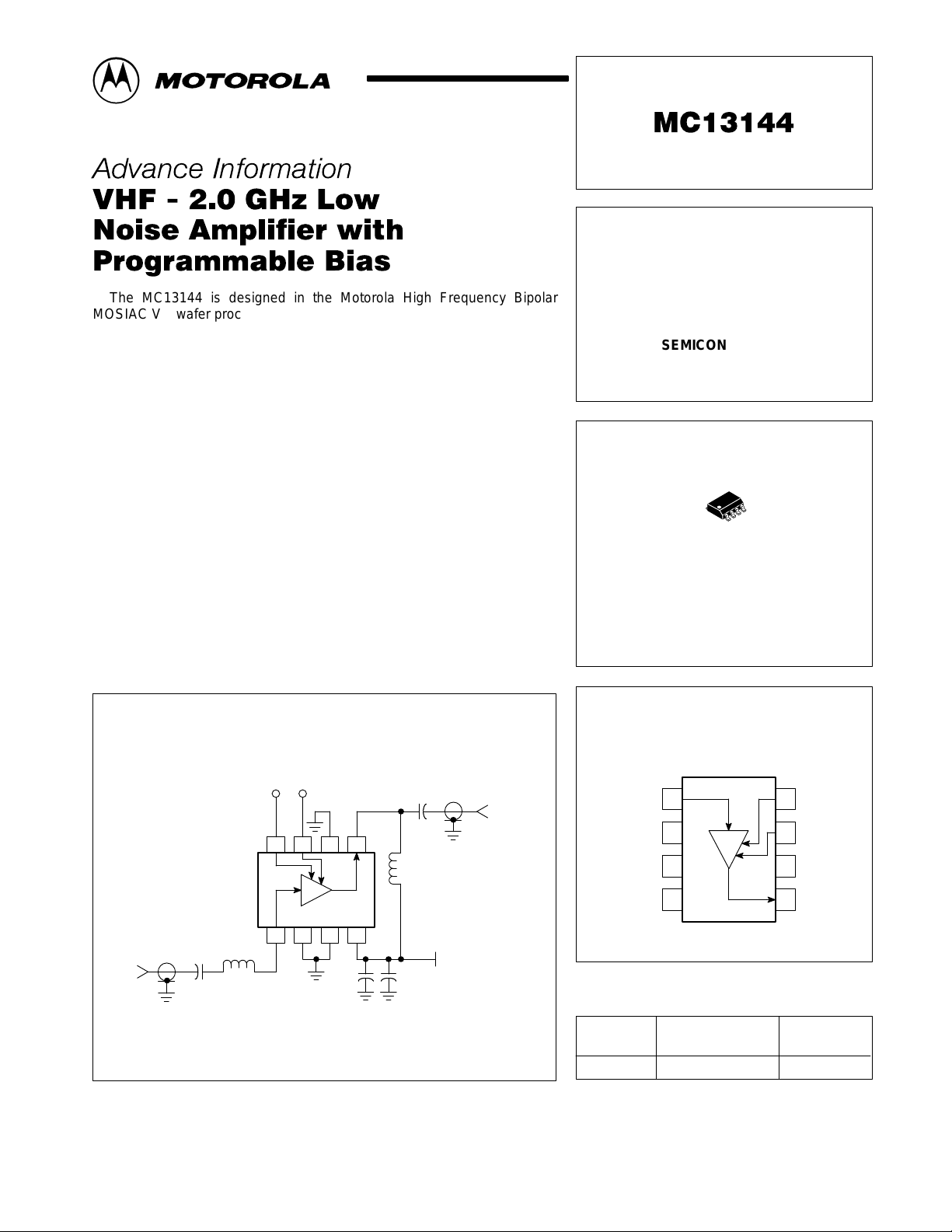
T ypical Application as 900 MHz Low Noise Amplifier
En2
En1
8
765
1234
RF
Input
47 p
5.6 nH
This device contains 67 active transistors.
1.6 p
8.2 nH
100 p100 n
PIN CONNECTIONS AND
FUNCTIONAL BLOCK DIAGRAM
1
RF
Output
V
CC
Device Package
MC13144D TA = – 40° to +85°C
In
V
2
EE
V
3
EE
V
4
CC
ORDERING INFORMATION
Operating
Temperature Range
En1
8
7
En2
V
6
EE
Out
5
SO–8
This document contains information on a new product. Specifications and information herein
are subject to change without notice.
MOTOROLA ANALOG IC DEVICE DATA
Motorola, Inc. 1997 Rev 0
1
MC13144
MAXIMUM RATINGS
Power Supply Voltage
Junction Temperature
Storage Temperature Range
NOTES: 1. Devices should not be operated at or outside these values. The “Recommended Operating
Conditions” provide for actual device operation.
2.ESD data available upon request.
RECOMMENDED OPERATING CONDITIONS
Power Supply Voltage V
Rating Symbol Value Unit
Rating
VCC(max)
T
Jmax
T
stg
7.0
+150
–65 to +150
Symbol Min Typ Max Unit
CC
Vdc
°C
°C
1.8 – 6.0 Vdc
DC ELECTRICAL CHARACTERISTICS (T
Characteristic
Supply Current (Power Down) I
(En1 = En2 = Low)
Supply Current (Power Up) I
(En1 = High; En2 = Low)
Supply Current (Power Up) I
(En1 = High; En2 = Low)
Supply Current (Power Up) I
(En1 = High; En2 = Low)
AC ELECTRICAL CHARACTERISTICS (T
Characteristic
Amplifier Gain (50 Ω Insertion Gain) S
(En1 = En2 = High)
Amplifier Reverse Isolation S12 – –35 – dB
(En1 = En2 = High)
Amplifier Input Return Loss Γin
(En1 = En2 = High)
Amplifier Output Return Loss Γout
(En1 = En2 = High)
Input 3rd Order Intercept Point (En1 = En2 = High) IIP3 dBm
df = 100 kHz – –11 –
df = 1.0 MHz – –5.0 –
Amplifier Noise Figure NF – 1.4 2.0 dB
(Figure 1; En1 = En2 = High)
Amplifier Gain @ NF G
(Figure 1; En1 = En2 = High)
Amplifier Gain (En1 = En2 = High) G
Amplifier Gain G
(En1 = High; En2 = Low)
Amplifier Gain G
(En1 = High; En2 = Low)
= 25°C; VCC = 3.0 Vdc; fRF = 1.0 GHz; Pin = –25 dBm)
A
Symbol Min Typ Max Unit
CC0
CC1
CC2
CC3
= 25°C; VCC = 3.0 Vdc; fRF = 1.0 GHz; Pin = –25 dBm)
A
Symbol Min Typ Max Unit
2
21
amp
amp
NF
ain3
ain2
ain1
– 0.0001 20 µA
– 1.2 2.0 mA
– 3.4 5.0 mA
– 8.2 12 mA
– 12 – dB
– –10 – dB
– –15 – dB
– 17 – dB
14 17 – dB
10 13.3 – dB
6.0 9.2 – dB
2
MOTOROLA ANALOG IC DEVICE DATA
MC13144
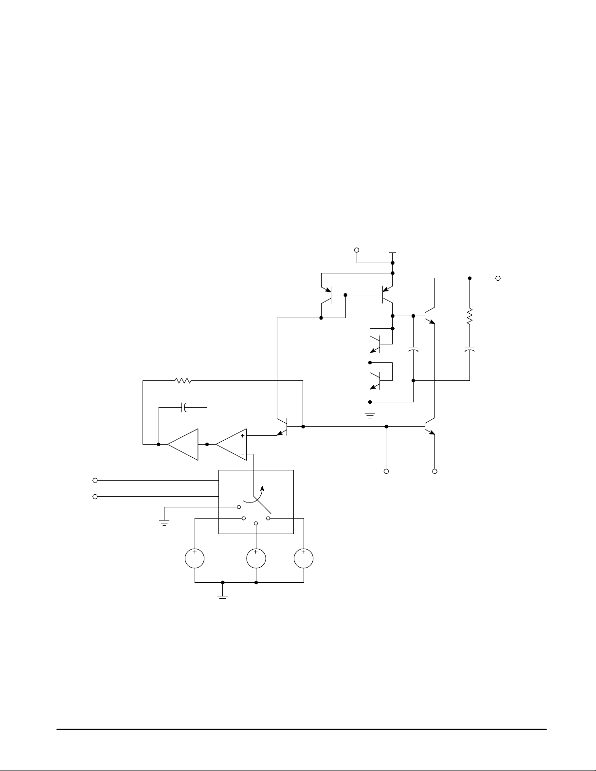
CIRCUIT DESCRIPTION
General
The MC13144 is a low noise amplifier with programmable
bias. This device is designated for use in the front end section
in analog and digital FM systems such as Wireless Local
Area Network (LAN), Digital European Cordless Telephone
(DECT), PHS, PCS, GPS, Cellular, UHF and 800 MHz
Special Mobile Radio (SMR), UHF Family Radio Services
and 902 to 928 MHz cordless telephones.
Current Regulation/Enable
Temperature compensating voltage independent current
regulation is digitally controlled by a 2 bit programmable
bias/enable circuit.
Figure 1. MC13144 Internal Circuit*
LNA
The LNA is a unique and patented cascode amplifier with
digitally (2 bit) programmable bias (see Internal Circuit
Schematic). Typical gain of the LNA is 17 dB for minimum
noise figure of 1.4 dB at 900 MHz.
Programmable Bias/Enable Circuit
This unique circuit allows for 3 bias levels and a standby
mode in which the LNA can be externally biased as desired.
4
V
CC
5
RF
Output
400
10 p
6
V
EE
–A
1 2, 3
En1
8
En2
7
V1
NOTE: * The MC13144 uses a unique and patent pending circuit topology.
V2
V3
RF In V
EE
MOTOROLA ANALOG IC DEVICE DATA
3
 Loading...