

Order this document by MC13143/D
The MC13143 is a high compression linear mixer with single–ended RF
input, differential IF output and differential LO inputs which consumes as
little as 1.8 mW. A new circuit topology is used to achieve a high third order
intermodulation intercept point, high linearity and high 1.0 dB output
compression point while maintaining a linear 50 Ω input impedance. It is
designed for Up or Down conversion anywhere from dc to 2.4 GHz.
Ultra Low Power: 1.0 mA @ VCC = 1.8 – 6.5 V
• Wide Input Bandwidth: DC–2.4 GHz
• Wide Output Bandwidth: DC–2.4 GHz
• Wide LO Bandwidth: DC–2.4 GHz
• High Mixer Linearity: P
Linearity Adjustment of up to IP
i1.0 dB
= 3.0 dBm
= 20 dBm
3in
• 50 Ω Mixer Input
• Single–Ended Mixer Input
• Double Balanced Mixer Operation
• Differential Open Collector Mixer Output
ULTRA LOW POWER DC –
2.4 GHz LINEAR MIXER
SEMICONDUCTOR
TECHNICAL DATA
8
1
D SUFFIX
PLASTIC PACKAGE
CASE 751
(SO–8)
PIN CONNECTIONS
ORDERING INFORMATION
Operating
Device
MC13143D TA = –40° to +85°C SO–8
MAXIMUM RATINGS (T
Rating
Power Supply Voltage VCC(max) 7.0 Vdc
Junction Temperature T
Storage Temperature Range T
NOTE: ESD data available upon request.
Temperature Range
= 25°C, unless otherwise noted.)
A
Symbol Value Unit
Jmax
stg
Package
+150 °C
–65 to +150 °C
1
Dec
Dec
2
V
CC
3
LO+ IF+
4
LO–
(Top View)
This device contains 29 active transistors.
8
RF
7
V
EE
6
5
IF–
This document contains information on a new product. Specifications and information herein
are subject to change without notice.
MOTOROLA ANALOG IC DEVICE DATA
Motorola, Inc. 1997 Rev 0
1
MC13143
RECOMMENDED OPERATING CONDITIONS
Rating
Power Supply Voltage V
Symbol Min Typ Max Unit
CC
1.8 – 6.0 Vdc
DC ELECTRICAL CHARACTERISTICS (T
Characteristic
Supply Current (Lin Control Current = 0) I
Supply Current (Lin Control Current = 1.6 mA) I
AC ELECTRICAL CHARACTERISTICS (T
Characteristic
Mixer Voltage Conversion Gain (RP = RL = 800 Ω) VG
Mixer Power Conversion Gain (RP = RL = 800 Ω) PG
Mixer Input Return Loss Γin
Mixer SSB Noise Figure NF
Mixer 1.0 dB Compression Point Pin
(Mx Lin Control Current = 1.6 mA)
Mixer Input Third Order Intercept Point IP3
(df = 1.0 MHz, I
LO Drive Level LO
LO Leakage to Mixer IF Outputs P
Mixer Input Feedthrough Output P
LO Leakage to Mixer Input P
Mixer Input Leakage to LO P
control
= 1.6 mA)
= 25°C, VCC = 3.0 V, fRF = 1.0 GHz, Pin = –25 dBm.)
A
Symbol Min Typ Max Unit
= 25°C, VCC = 3.0 V, fRF = 1.0 GHz, Pin = –25 dBm.)
A
Symbol Min Typ Max Unit
LO–RFm
RFm–LO
CC1
CC2
C
C
mx
SSB
–1.0 dB
in
in
LO–IF
RFm–IF
– 1.0 – mA
– 4.1 – mA
– 9.0 – dB
–3.5 –2.6 –1.5 dB
– –20 – dB
– 14 15 dB
–1 0 – dBm
– 16 – dBm
– –5.0 – dBm
– –33 –25 dB
– –25 – dB
– –40 –25 dB
– –35 – dB
LO
100 p100 n
100 n 100 p
100 p
100 p
Dec
V
CC
50 50
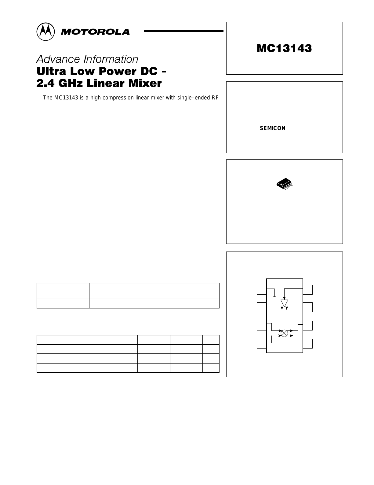
Figure 1. T est Circuit
I
Adjust
1
Dec
2
3
4
V
CC
RF
8
100 p
7
6
5
V
800
EE
16
IF
1
2
MOTOROLA ANALOG IC DEVICE DATA
MC13143
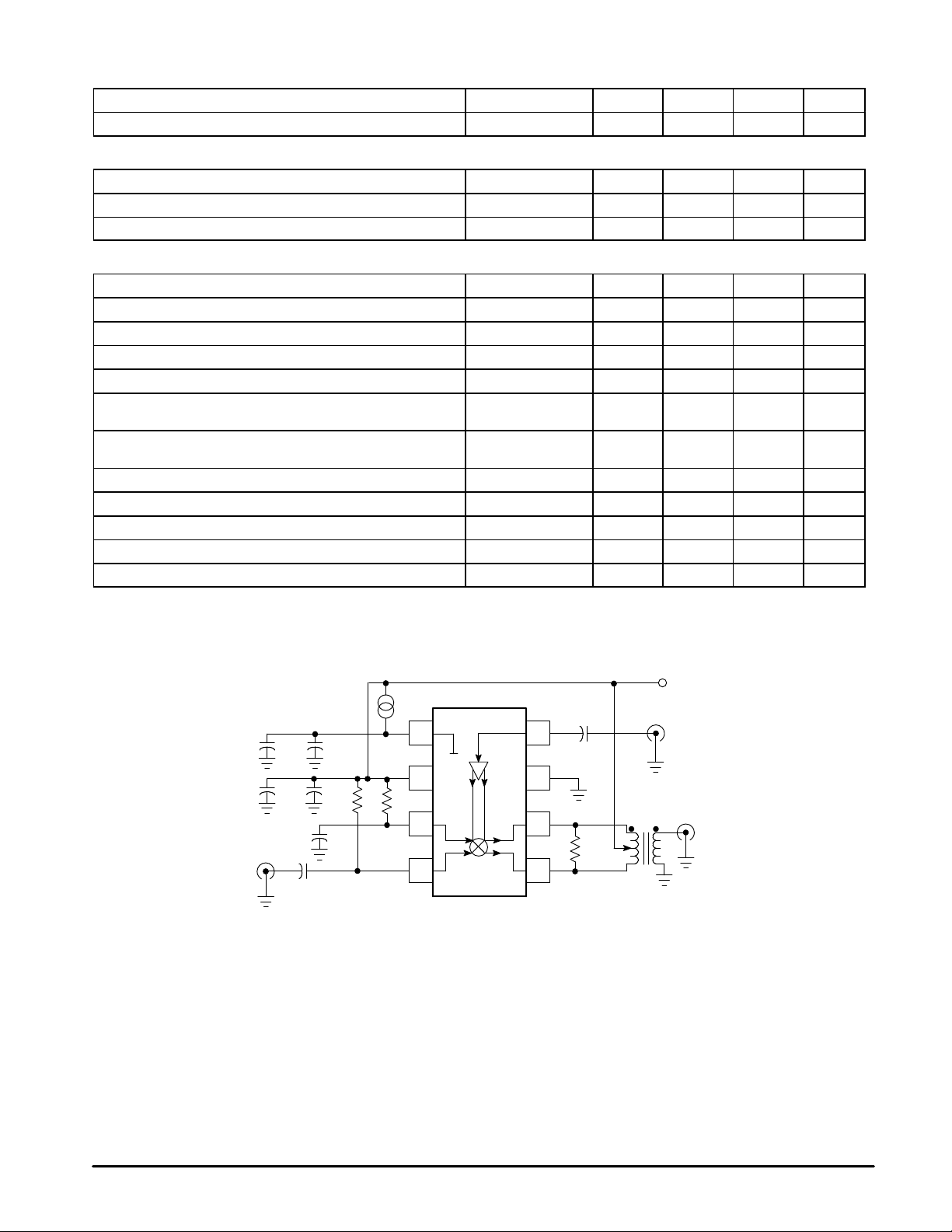
TYPICAL PERFORMANCE CURVES
0
–2.0
–4.0
GAIN (dB)
–6.0
–8.0
–10
0
0
–5.0
Figure 2. Power Conversion Gain and
Supply Current versus Supply V oltage
2.0
4.0
VS (Vdc)
6.0 8.0
Figure 4. Mixer Input Return Loss
versus RF Input Frequency
2.0
1.6
1.2
0.8
0.4
0
(mA)
S
I
Figure 3. Noise Figure and Gain
versus LO Power
13.2
13
12.8
(dB)
12.6
SSB
12.4
N F
12.2
12
11.8
–1.0
–5.0
LO POWER (dBm)
0
Figure 5. Power Conversion Gain and Supply
Current versus RF Input Power
– 4.5
– 5.5
fRF = 900 MHz
fLO = 950 MHz
Test Circuit
5.0
–3.0
–3.2
–3.4
–3.6
–3.8
–4.0
–4.2
–4.4
8.0
6.0
GAIN (dB)
–10
–15
–20
MIXER RF INPUT RETURN LOSS (dB)
–25
0
0.5
Figure 6. Noise Figure and Gain
15.5
14.5
13.5
(dB)
SSB
12.5
N F
11.5
1.0
RF INPUT FREQUENCY (GHz)
1.5
2.0
versus RF Frequency
2.5
–4.0
–5.0
–6.0
–7.0
V = 5.0 Vdc
– 6.5
fRF = 900 MHz
fLO = 950 MHz
GAIN (dB)
PLO = 0 dBm
Test Circuit
– 7.5
– 8.5
–30
Figure 7. IIP3, Gain, Supply Current
versus Mixer Linearity Control Current
25
20
VS = 5.0 Vdc
(mA)
S
15
fRF = 900 MHz
fLO = 950 MHz
10
5.0
GAIN (dB)
0
IIP3 (dBm), GAIN (dB), I
–5.0
– 20 – 10 0 10
RF INPUT POWER (dBm)
IIP3 (dBm)
IS(mA)
GAIN(dB)
4.0
2.0
0
(mA)
S
I
10.5
0
0.5 1.0 1.5 2.0
RF FREQUENCY (GHz)
MOTOROLA ANALOG IC DEVICE DATA
2.5
–8.0
–10
–5
10
MIXER LINEARITY CONTROL CURRENT, IMx
10
–4
10
–3
Lin Cont
(A)
10
–2
3

MC13143
CIRCUIT DESCRIPTION
General
The MC13143 is a double–balanced Mixer. This device is
designated for use as the frontend section in analog and
digital FM systems such as Wireless Local Area Network
(LAN), Digital European Cordless Telephone (DECT), PHS,
PCS, GPS, Cellular, UHF and 800 MHz Special Mobile
Radio (SMR), UHF Family Radio Services and 902 to
928 MHz cordless telephones. It features a mixer linearity
control to preset or auto program the mixer dynamic range,
an enable function and a wideband IF so the IC may be
used either as a down converter or an up converter.
Current Regulation
Temperature compensating voltage independent current
regulators provide typical supply current at 1.0 mA with no
mixer linearity control current.
Figure 8. MC13143 Internal Circuit*
4
LO–
1.0 k
1.0 k
Mixer
The mixer is a unique and patented double–balanced four
quadrant multiplier biased class AB allowing for
programmable linearity control via an external current
source. An input third order intercept point of 20 dBm may be
achieved. All 3 ports of the mixer are designed to work up to
2.4 GHz. The mixer has a 50 Ω single–ended RF input and
open collector differential IF outputs (see Internal Circuit
Schematic for details). The linear gain of the mixer is
approximately –5.0 dB with a SSB noise figure of 12 dB.
Local Oscillator
The local oscillator has differential input configuration that
requires typically –10 dBm input from an external source to
achieve the optimal mixer gain.
IF–
5
IF+
6
V
CC
2
7
V
EE
Q0 Q1 Q2 Q3
3
LO+
V
CC
V
1
Mx Lin
Cont
NOTE: * The MC13143 uses a unique and patented circuit topology.
EE
Q7 Q4
Q6
Q5
V
ref1
33
33
400 µA
8
RF
m
4
MOTOROLA ANALOG IC DEVICE DATA

MC13143
APPLICATIONS INFORMATION
Evaluation PC Board
The evaluation PCB is very versatile and is intended to be
used across the entire useful frequency range of this device.
The PC board is laid out to accommodate all SMT
components on the circuit side (see Circuit Side Component
Placement View).
Component Selection
The evaluation PC board is designed to accommodate
specific components, while also being versatile enough to
use components from various manufacturers. The circuit side
placement view is illustrated for the components specified in
the application circuit. The Component Placement View
specifies particular components that were used to achieve
the results shown in the typical curves and tables.
Mixer Input
The mixer input impedance is broadband 50 Ω for
applications up to 2.4 GHz. It easily interfaces with a RF
ceramic filter as shown in the application schematic.
Mixer Linearity Control
The mixer linearity control circuit accepts approximately
0 to 2.3 mA control current. An Input Third Order Intercept
Point, IIP3 of 20 dBm may be achieved at 2.3 mA of control
current (approximately 7.0 mA of additional supply current).
Local Oscillator Inputs
The differential LO inputs are internally biased at
V
– 1.0 VBE; this is suitable for high voltage and high gain
CC
operation.
For low voltage operation, the inputs are taken to V
CC
through 51 Ω.
IF Output
The IF is a differential open collector configuration which is
designed to use over a wide frequency range for up
conversion as well as down conversion.
Input/Output Matching
It is desirable to use a RF ceramic or SAW filter before the
mixer to provide image frequency rejection. The filter is
selected based on cost, size and performance tradeoffs.
Typical RF filters have 3.0 to 5.0 dB insertion loss. The PC
board layout accommodates both ceramic and SAW RF
filters which are offered by various suppliers such as
Siemens, Toko and Murata.
Interface matching between the RF input, RF filter and the
mixer will be required. The interface matching networks
shown in the application circuit are designed for 50 Ω
interfaces.
Differential to single–ended circuit configuration is shown
in the test circuit. 6.0 dB of additional mixer gain can be
achieved by conjugately matching the output of the
MiniCircuits transformer to 50 Ω at the desired IF frequency.
With narrowband IF output matching the mixer performance
is 3.0 dB gain and 12 dB noise figure (see Narrowband 49
and 83 MHz IF Output Matching Options). Typical insertion
loss of the T oko ceramic filter is 3.0 dB. Thus, the overall gain
of the circuit is 0 dB with a 15 dB noise figure.
Figure 9. Narrowband IF Output Matching with
16:1 Z Transformer and LC Network
10 n
9.2 k
SMA
330 nH
36 p
SMA
Mixer
RF Input
49 MHz
IF
Output
SMA
Mixer
RF Input
83.16 MHz
IF
Output
Mixer
Mixer
IF
Outputs
IF
Outputs
8
7
6
5
8
7
6
5
180
nH
100 p
V
CC
Z Transformer
16:1
100 p
V
CC
180 nH
9.2 p
V
CC
MOTOROLA ANALOG IC DEVICE DATA
5

MC13143
Figure 10. Circuit Side Component Placement View
MC13143D
IF
Out
Mixer In
Toko
926A10
Dielectric
Filter
16:1
Impedance
Transformer
820
Gnd
Mx Lin
Cont
100 n
100 p
MC13143D
51
100 n
100 p
51
100 n
100 p
100 p
V
CC
LO
Input
Rev A
NOTES: 926.5 MHz preselect dielectric filter is Toko part # 4DFA–926A10; the 4DF A (2 and 3 pole SMD type) filters are available
for applications in cellular and GSM, GPS, DECT , PHS, PCS and ISM bands at 902–928 MHz, 1.8–1.9 GHz at 2.4–2.5 GHz.
The PCB also accommodates a surface mount RF SAW filter in an eight or six pin ceramic package for the cellular base and
handset frequencies. Recommended manufacturers are Siemens and Murata.
The PCB may also be used without a preselector filter; AC coupled to the mixer as shown in the test circuit schematic.
All other external circuit components shown in the PCB layout above are the same as used in the test circuit schematic.
16:1 broadband impedance transformer is mini circuits part #TX16–R3T; it is in the leadless surface mount “TX” package. For a
more selective narrowband match, a lowpass filter may be used after the transformer. The PCB is designed to accommodate
lump inductors and capacitors in more selective narrowband matching of the mixer differential outputs to a single–ended output
at a given IF frequency.
. The local oscillator may also be driven in a differential configuration using a coaxial transformer . Recommended sources are the
T oko Balun transformers type B4F, B5FL and B5F (SMD component).
6
MOTOROLA ANALOG IC DEVICE DATA

Mixer In
Mx Lin
Cont
MC13143
Figure 11. Circuit Side V iew
MC13143D
IF
Out
Gnd
V
CC
Rev A
NOTES: Critical dimensions are 50 mil centers lead to lead in SO–8 footprint.
Also line widths to labeled ports excluding VCC are 50 mil.
LO
Input
Figure 12. Ground Side View
Rev A
Mx Lin
Cont
V
CC
LO
Input
Mixer In
MC13143D
MOTOROLA ANALOG IC DEVICE DATA
IF
Out
7

MC13143
OUTLINE DIMENSIONS
D SUFFIX
PLASTIC PACKAGE
CASE 751–06
(SO–8)
ISSUE T
A
C
A1
D
58
0.25MB
E
1
B
e
H
4
M
h
X 45
_
q
C
A
SEATING
PLANE
0.10
L
B
SS
A0.25MCB
NOTES:
1. DIMENSIONING AND TOLERANCING PER ASME
Y14.5M, 1994.
2. DIMENSIONS ARE IN MILLIMETER.
3. DIMENSION D AND E DO NOT INCLUDE MOLD
PROTRUSION.
4. MAXIMUM MOLD PROTRUSION 0.15 PER SIDE.
5. DIMENSION B DOES NOT INCLUDE DAMBAR
PROTRUSION. ALLOWABLE DAMBAR
PROTRUSION SHALL BE 0.127 TOTAL IN EXCESS
OF THE B DIMENSION AT MAXIMUM MATERIAL
CONDITION.
MILLIMETERS
DIM MIN MAX
A 1.35 1.75
A1 0.10 0.25
B 0.35 0.49
C 0.19 0.25
D 4.80 5.00
E
3.80 4.00
1.27 BSCe
H 5.80 6.20
h
0.25 0.50
L 0.40 1.25
0 7
q
__
Motorola reserves the right to make changes without further notice to any products herein. Motorola makes no warranty , representation or guarantee regarding
the suitability of its products for any particular purpose, nor does Motorola assume any liability arising out of the application or use of any product or circuit, and
specifically disclaims any and all liability, including without limitation consequential or incidental damages. “T ypical” parameters which may be provided in Motorola
data sheets and/or specifications can and do vary in different applications and actual performance may vary over time. All operating parameters, including “Typicals”
must be validated for each customer application by customer’s technical experts. Motorola does not convey any license under its patent rights nor the rights of
others. Motorola products are not designed, intended, or authorized for use as components in systems intended for surgical implant into the body, or other
applications intended to support or sustain life, or for any other application in which the failure of the Motorola product could create a situation where personal injury
or death may occur. Should Buyer purchase or use Motorola products for any such unintended or unauthorized application, Buyer shall indemnify and hold Motorola
and its officers, employees, subsidiaries, affiliates, and distributors harmless against all claims, costs, damages, and expenses, and reasonable attorney fees
arising out of, directly or indirectly, any claim of personal injury or death associated with such unintended or unauthorized use, even if such claim alleges that
Motorola was negligent regarding the design or manufacture of the part. Motorola and are registered trademarks of Motorola, Inc. Motorola, Inc. is an Equal
Opportunity/Affirmative Action Employer.
How to reach us:
USA/EUROPE/Locations Not Listed: Motorola Literature Distribution; JAPAN: Nippon Motorola Ltd.: SPD, Strategic Planning Office, 4–32–1,
P.O. Box 5405, Denver, Colorado 80217. 1–303–675–2140 or 1–800–441–2447 Nishi–Gotanda, Shinagawa–ku, Tokyo 141, Japan. 81–3–5487–8488
Customer Focus Center: 1–800–521–6274
Mfax: RMFAX0@email.sps.mot.com – TOUCHTONE 1–602–244–6609 ASIA/PACIFIC: Motorola Semiconductors H.K. Ltd.; 8B Tai Ping Industrial Park,
Moto rola Fax Back Syst em – US & Canada ONLY 1–800–774–1848 51 Ting Kok Road, Tai Po, N.T., Hong Kong. 852–26629298
HOME PAGE: http://motorola.com/sps/
8
– http://sps.motorola.com/mfax/
◊
MOTOROLA ANALOG IC DEVICE DATA
Mfax is a trademark of Motorola, Inc.
MC13143/D
 Loading...