

Motorola MC13142D Datasheet
Order this document By MC13142/D
The MC13142 is intended to be used as a first amplifier, voltage controlled
oscillator and down converter for RF applications. It features wide band
operation, low noise, high gain and high linearity while maintaining low
current consumption. The circuit consists of a Low Noise Amplifier (LNA), a
Voltage Controlled Oscillator (VCO), a buf fered oscillator output, a mixer, an
Intermediate Frequency amplifier (IF
mixer IF bandwidth allows this part also to be used as an up converter and
exciter amplifier.
• Wide RF Bandwidth: DC–1.8 GHz
• Wide LO Bandwidth: DC–1.8 GHz
• Wide IF Bandwidth: DC–1.8 GHz
• Low Power: 13 mA @ V
• High Mixer Linearity: P
= 2.7 – 6.5 V
CC
i1.0 dB
= 3.0 dBm
• Linearity Adjustment Increases IP
• Single–Ended 50 Ω Mixer Input
• Double Balanced Mixer Operation
• Open Collector Mixer Output
• Single Transistor Oscillator with Collector, Base and Emitter Pinned Out
• Buffered Oscillator Output
) and a dc control section. The wide
amp
Up to 20 dBm
3in
LOW POWER DC – 1.8 GHz
LNA, MIXER and VCO
SEMICONDUCTOR
TECHNICAL DATA
16
1
D SUFFIX
PLASTIC PACKAGE
CASE 751B
(SO–16)
PIN CONNECTIONS
SO–16
EN
1
RF
2
in
V
3
EE
Osc E
4
Osc B
5
Osc C, V
This device contains 176 active transistors.
This document contains information on a new product. Specifications and information herein
are subject to change without notice.
MOTOROLA RF/IF DEVICE DATA
V
CC
Buff
CC
6
7
8
Mx Lin
Cont
RF
16
V
15
CC
Mix Lin Cont
14
RF
13
V
EE
12
IF+
11
IF–
10
9
V
EE
out
m
ORDERING INFORMATION
Operating
Device
MC13142D TA = –40° to +85°C SO–16
Motorola, Inc. 1998 Rev 1
Temperature Range
Package
1
MC13142
A
mA
MAXIMUM RATINGS (T
Power Supply Voltage V
Operating Supply Voltage Range V
NOTE: ESD data available upon request.
ELECTRICAL CHARACTERISTICS (V
Supply Current (Disable) I
Pin 15 with Pin 1 @ 0 V I
Pin 10 and 11 with Pin 1 @ 0 V I
Pin 6 with Pin 1 @ 0 V I
Supply Current (Enable) I
Pin 15 with Pin 1 @ 3.0 V I
Pin 10 with Pin 1 @ 3.0 V I
Pin 6 with Pin 1 @ 3.0 V I
Amplifier Gain (50 Ω Insertion Gain) S
Amplifier Reverse Isolation S
Amplifier Input Match Γin
Amplifier Output Match Γ
Amplifier 1.0 dB Gain Compression Pin
Amplifier Input Third Order Intercept IP3
Amplifier Noise Figure (Application Circuit) NF 1.0 1.8 4.0 dB
Amplifier Gain @ N.F. G
Mixer Voltage Conversion Gain (RP = RL = 800 Ω) VG
Mixer Power Conversion Gain (RP = RL = 800 Ω) PG
Mixer Input Match Γin
Mixer SSB Noise Figure NF
Mixer 1.0 dB Gain Compression Pin
Mixer Input Third Order Intercept IP3
Oscillator Buffer Drive (50 Ω) P
Oscillator Phase Noise @ 25 kHz Offset N
RFin Feedthrough to RF
RF
Feedthrough to RF
out
LO Feedthrough to IF P
LO Feedthrough to RF
LO Feedthrough to RF
Mixer RF Feedthrough to IF P
Mixer RF Feedthrough to RF
= 25°C, unless otherwise noted.)
A
Rating
= 3.0 V, TA = 25°C, LOin = –10 dBm @ 950 MHz, IF @ 50 MHz.)
CC
Characteristic Symbol Min Typ Max Unit
m
m
in
m
in
Symbol Value Unit
CC(max)
CC
7.0 Vdc
2.7 to 6.5 Vdc
CC_Total
CC_15
CC_Mix
CC_6
CC_Total
CC_15
CC_Mix
CC_6
21
12
amp
out amp
–1.0 dB
in
NF
C
C
M
SSBM
–1.0 dBM
InM
VCO
Φ
P
RFin–RFm
P
RFout–RFm
LO–IF
P
LO–RFin
P
LO–RFm
RFm–IF
P
RFm–RFin
–230 – 230
–110 – 110
–20 – 20
–100 – 100
8.25 13.5 26
1.0 – 4.5
1.25 – 7.5
6.0 – 14
6.5 12 13 dB
– –33 – dB
– –10 – dB
– –15 – dB
–18 –15 –8.0 dBm
– –5.0 – dBm
– 17 – dB
– 9.0 – dB
–7.0 –3.0 –2.0 dB
– –20 – dB
– 12 – dB
– 3.0 – dBm
– –1.0 – dBm
–19.5 –16 –12 dBm
– –90 – dBc/Hz
– –35 – dB
– –35 – dB
– –35 – dBm
– –35 – dBm
– –35 – dBm
– –25 – dB
– –25 – dB
µ
2
MOTOROLA RF/IF DEVICE DATA

MC13142
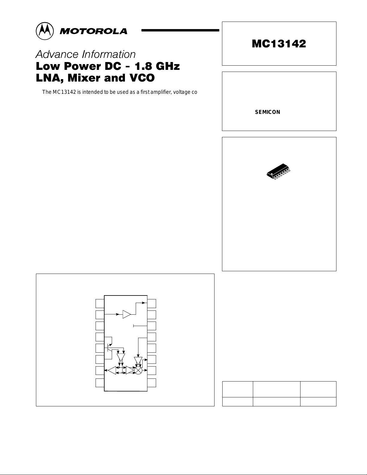
CIRCUIT DESCRIPTION
General
The MC13142 is a low power LNA, double–balanced
Mixer, and VCO. This device is designated for use as the
frontend section in analog and digital FM systems such as
Digital European Cordless Telephone (DECT), PHS, PCS,
Cellular, UHF and 800 MHz Special Mobile Radio (SMR),
UHF Family Radio Services and 902 to 928 MHz cordless
telephones. It features a mixer linearity control to preset or
auto program the mixer dynamic range, an enable function
and a wideband IF so the IC may be used either as a down
converter or an up converter. Further details are covered in
the Pin by Pin Description which shows the equivalent
internal circuit and external circuit requirements.
Current Regulation/Enable
Temperature compensating voltage independent current
regulators are controlled by the enable function in which
“high” powers up the IC.
Low Noise Amplifier (LNA)
The LNA is internally biased at low supply current
(approximately 2.0 mA emitter current) for optimal noise
figure and gain. The LNA output is biased internally with a
600 Ω resistor to VCC. Input and output matching may be
achieved at various frequencies using few external
components. Matching the LNA for Maximum stable gain
(MSG) yields noise performance within a few tenths of a dB
of the minimum noise figure.
Mixer
The mixer is a double–balanced four quadrant multiplier
biased class AB allowing for programmable linearity control
via an external current source. An input third order intercept
point of 20 dBm may be achieved. All 3 ports of the mixer are
designed to work up to 1.8 GHz. The mixer has a 50 Ω
single–ended RF input and open collector differential IF
outputs. An on–board Local Oscillator transistor has the
emitter, base and collector pinned out to implement a low
phase noise VCO in various configurations. Additionally, a
buffered LO output is provided for operation with a frequency
synthesizer. The linear gain of the mixer is approximately
0 dB with a SSB noise figure of 12 dB in the IF output circuit
configuration shown in the application example.
Local Oscillator
The on–chip transistor operates with coaxial transmission
line or LC resonant elements to over 2.0 GHz. Biasing is
done with a temperature compensated current source in the
emitter and a collector to base internal resistor of 7.6 kΩ;
however, an RFC from VCC to base is recommended. The
application circuit shows a voltage controlled Clapp oscillator
operating at center frequency of 975 MHz.
MOTOROLA RF/IF DEVICE DATA
3
MC13142
Á
Á
Á
Á
Á
Á
Á
Á
Á
Á
Á
Á
Á
Á
Á
Á
Á
Á
Á
Á
Á
Á
Á
Á
Á
Á
Á
Á
Á
Á
Á
Á
Á
Á
Á
Á
Á
Á
Á
Á
Á
Á
RF
V
Á
Á
Á
Á
Á
Á
Á
Á
Á
Á
Á
Á
Á
Á
Á
Á
Á
Á
Á
Á
Á
Á
Á
Á
Á
Á
Á
Á
Á
Á
Á
Á
Á
Á
Á
Á
Á
Osc C
Á
Á
Á
Á
Á
Á
Á
Á
Á
Á
Á
Á
Á
LO Buf
Á
Á
Á
Á
Pin
16 Pin
SOIC
1
ÁÁÁ
ÁÁÁ
ÁÁÁ
ÁÁÁ
ÁÁÁ
ÁÁÁ
ÁÁÁ
ÁÁÁ
ÁÁÁ
ÁÁÁ
2
ÁÁÁ
ÁÁÁ
3
ÁÁÁ
ÁÁÁ
ÁÁÁ
16
ÁÁÁ
ÁÁÁ
Symbol
EN
ÁÁ
ÁÁ
ÁÁ
ÁÁ
ÁÁ
ÁÁ
ÁÁ
ÁÁ
ÁÁ
ÁÁ
RF
in
ÁÁ
ÁÁ
V
EE
ÁÁ
ÁÁ
ÁÁ
RF
out
ÁÁ
ÁÁ
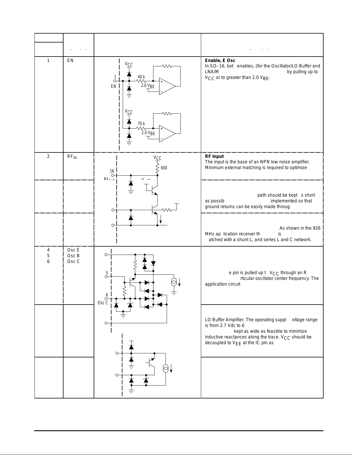
PIN FUNCTION DESCRIPTION
Equivalent Internal Circuit
(20 Pin LQFP)
V
CC
40 k1
2.0 V
V
CC
70 k
2.0 V
ref2
V
EE
RF
V
EN
16
out
2
in
3
EE
BE
BE
Description
Enable, E Osc
In SO–16, both enables, (for the Oscillator/LO Buffer and
БББББББББББББ
LNA/Mixer) are bonded to Pin 1. Enable by pulling up to
VCC or to greater than 2.0 VBE.
БББББББББББББ
БББББББББББББ
БББББББББББББ
БББББББББББББ
БББББББББББББ
БББББББББББББ
БББББББББББББ
БББББББББББББ
БББББББББББББ
V
CC
600
RF Input
The input is the base of an NPN low noise amplifier.
БББББББББББББ
Minimum external matching is required to optimize the
input return loss and gain.
БББББББББББББ
VEE – Negative Supply
VEE pin is taken to an ample dc ground plane through a
БББББББББББББ
low impedance path. The path should be kept as short
as possible. A two sided PCB is implemented so that
БББББББББББББ
ground returns can be easily made through via holes.
БББББББББББББ
RF Output
The output is from the collector of the LNA; it is internally
БББББББББББББ
biased with a 600 Ω resistor to VCC. As shown in the 926
MHz application receiver the output is conjugately
БББББББББББББ
matched with a shunt L, and series L and C network.
2.0 mA
V
ref3
ÁÁÁ
ÁÁÁ
ÁÁÁ
ÁÁÁ
ÁÁÁ
ÁÁÁ
ÁÁÁ
ÁÁÁ
ÁÁÁ
ÁÁÁ
ÁÁÁ
ÁÁÁ
ÁÁÁ
ÁÁÁ
ÁÁÁ
4
5
6
6
8
7
4
Osc E
ÁÁ
Osc B
Osc C
ÁÁ
ÁÁ
ÁÁ
ÁÁ
ÁÁ
V
CC
V
CC
ÁÁ
ÁÁ
ÁÁ
ÁÁ
ÁÁ
LO Buff
ÁÁ
ÁÁ
ÁÁ
ÁÁ
4
Osc E
5
Osc B
6
Osc C
6
V
CC
V
7.6 k
7
8
CC
On–Board VCO Transistor
БББББББББББББ
10
The transistor has the emitter, base and collector + V
pins available. Internal biasing which is compensated for
БББББББББББББ
stability over temperature is provided. It is recommended
БББББББББББББ
that the base pin is pulled up to VCC through an RFC
1.5
mA
V
EE
chosen for the particular oscillator center frequency. The
БББББББББББББ
application circuit shows a modified Colpitts or Clapp
БББББББББББББ
oscillator configuration and its design is discussed in
detail in the application section.
БББББББББББББ
CC
Supply Voltage (VCC)
V
EE
V
CC
Two VCC pins are provided for the Local Oscillator and
БББББББББББББ
LO Buffer Amplifier. The operating supply voltage range
БББББББББББББ
is from 2.7 Vdc to 6.5 Vdc. In the PCB layout, the V
trace must be kept as wide as feasible to minimize
БББББББББББББ
inductive reactances along the trace. VCC should be
БББББББББББББ
decoupled to VEE at the IC pin as shown in the
component placement view.
БББББББББББББ
CC
Local Oscillator Buffer
1.0
mA
V
EE
This is a buffered output providing –16 dBm
БББББББББББББ
(50 Ω termination) to drive the fin pin of a PLL
БББББББББББББ
synthesizer. Impedance matching to the synthesizer may
be necessary to deliver the optimal signal and to
БББББББББББББ
improve the phase noise performance of the VCO.
БББББББББББББ
MOTOROLA RF/IF DEVICE DATA
Pin
Á
Á
Á
Á
Á
Á
Á
Á
Á
Á
Á
Á
Á
Á
Á
Á
Á
Á
Á
Á
Á
Á
Á
Á
Á
Á
Á
Á
Á
Á
Á
Á
Á
Á
Á
Á
Á
Á
Á
Á
Á
Á
Á
Á
Á
Á
Á
Á
Á
Á
Á
Á
Á
Á
Á
Á
Á
Á
Á
Á
Á
Á
Á
Á
Á
Á
16 Pin
SOIC
9, 12
ÁÁÁ
ÁÁÁ
ÁÁÁ
10, 11
ÁÁÁ
ÁÁÁ
ÁÁÁ
ÁÁÁ
ÁÁÁ
Symbol
Symbol
V
EE
ÁÁ
ÁÁ
ÁÁ
IF–, IF+
ÁÁ
ÁÁ
ÁÁ
ÁÁ
ÁÁ
PIN FUNCTION DESCRIPTION (continued)
Equivalent Internal Circuit
Equivalent Internal Circuit
(20 Pin LQFP)
(20 Pin LQFP)
10
IF–
9
V
V
CC
EE
11
IF+
12
V
EE
MC13142
V
CC
Description
Description
VEE, Negative Supply
These pins are VEE supply for the mixer IF output. In the
БББББББББББББ
application PC board these pins are tied to a common
VEE trace with other VEE pins.
БББББББББББББ
БББББББББББББ
IF Output
The IF is a differential open collector configuration which
БББББББББББББ
designed to use over a wide frequency range for up
conversion as well as down conversion. Differential to
БББББББББББББ
single–ended circuit configuration and matching options
БББББББББББББ
are discussed in the application section. 6.0 dB of
additional Mixer gain can be achieved by conjugately
БББББББББББББ
matching at the desired IF frequency.
БББББББББББББ
13
ÁÁÁ
ÁÁÁ
ÁÁÁ
ÁÁÁ
ÁÁÁ
ÁÁÁ
14
ÁÁÁ
ÁÁÁ
ÁÁÁ
ÁÁÁ
ÁÁÁ
ÁÁÁ
ÁÁÁ
ÁÁÁ
15 V
RF
m
ÁÁ
ÁÁ
ÁÁ
ÁÁ
ÁÁ
ÁÁ
Mix Lin
ÁÁ
Cont
ÁÁ
ÁÁ
ÁÁ
ÁÁ
ÁÁ
ÁÁ
ÁÁ
CC
13
RF
m
14
Mix Lin
Cont
15
V
CC
V
CC
V
ref1
V
EE
33
The mixer input impedance is broadband 50 Ω for
БББББББББББББ
applications up to 1.8 GHz. It easily interfaces with a RF
БББББББББББББ
ceramic filter as shown in the application schematic.
БББББББББББББ
БББББББББББББ
БББББББББББББ
БББББББББББББ
Mixer Linearity Control
Mixer RF Input
БББББББББББББ
The mixer linearity control circuit accepts approximately
0 to 2.3 mA control current to set the dynamic range of
БББББББББББББ
the mixer. An Input Third Order Intercept Point, IIP3 of
БББББББББББББ
20 dBm may be achieved at 2.3 mA of control current
(approximately 7.0 mA of additional supply current).
БББББББББББББ
БББББББББББББ
БББББББББББББ
БББББББББББББ
БББББББББББББ
400
33
µ
A
VCC, Power Supply
V
CC
MOTOROLA RF/IF DEVICE DATA
5
 Loading...