

Motorola MC13135P, MC13136DW, MC13136P, MC13135DW Datasheet
Operating
Temperature Range
DUAL CONVERSION
NARROWBAND
FM RECEIVERS
ORDERING INFORMATION
P SUFFIX
PLASTIC PACKAGE
CASE 724
Order this document by MC13135/D
DW SUFFIX
PLASTIC PACKAGE
CASE 751E
(SO–24L)
24
1
24
1
Device Package
MC13135P
MC13135DW
TA = – 40° to +85°C
Plastic DIP
SO–24L
MC13136P
MC13136DW
Plastic DIP
SO–24L
1
MOTOROLA ANALOG IC DEVICE DATA
The MC13135/MC13136 are the second generation of single chip, dual
conversion FM communications receivers developed by Motorola. Major
improvements in signal handling, RSSI and first oscillator operation have
been made. In addition, recovered audio distortion and audio drive have
improved. Using Motorola’s MOSAIC 1.5 process, these receivers offer
low noise, high gain and stability over a wide operating voltage range.
Both the MC13135 and MC13136 include a Colpitts oscillator, VCO tuning
diode, low noise first and second mixer and LO, high gain limiting IF, and
RSSI. The MC13135 is designed for use with an LC quadrature detector and
has an uncommitted op amp that can be used either for an RSSI buffer or as
a data comparator. The MC13136 can be used with either a ceramic
discriminator or an LC quad coil and the op amp is internally connected for a
voltage buffered RSSI output.
These devices can be used as stand–alone VHF receivers or as the lower
IF of a triple conversion system. Applications include cordless telephones,
short range data links, walkie–talkies, low cost land mobile, amateur radio
receivers, baby monitors and scanners.
• Complete Dual Conversion FM Receiver – Antenna to Audio Output
• Input Frequency Range – 200 MHz
• Voltage Buffered RSSI with 70 dB of Usable Range
• Low Voltage Operation – 2.0 to 6.0 Vdc (2 Cell NiCad Supply)
• Low Current Drain – 3.5 mA Typ
• Low Impedance Audio Output < 25 Ω
• VHF Colpitts First LO for Crystal or VCO Operation
• Isolated Tuning Diode
• Buffered First LO Output to Drive CMOS PLL Synthesizer
23
22
21
20
19
18
17
16
15
14
13
12
11
10
9
8
7
6
5
4
3
2
1
24
AF
VCC2
2nd LO
VCC1
1st LO
Varicap
Limiter
Demod
1st LO Base
1st LO Emitter
1st LO Out
VCC1
2nd LO Emitter
2nd LO Base
2nd Mixer Out
V
EE
Limiter In
Decouple 1
Decouple 2
RSSI
Varicap C
Varicap A
1st Mixer In 1
1st Mixer In 2
1st Mixer Out
VCC2
2nd Mixer In
Audio Out
Op Amp Out
Op Amp In –
Op Amp In +
Quad Coil
23
22
21
20
19
18
17
16
15
14
13
12
11
10
9
8
7
6
5
4
3
2
1
24
AF
V
CC2
2nd LO
VCC1
1st LO
Varicap
Limiter
Demod
1st LO Base
1st LO Emitter
1st LO Out
VCC1
2nd LO Emitter
2nd LO Base
2nd Mixer Out
V
EE
Limiter In
Decouple 1
Decouple 2
RSSI
Varicap C
Varicap A
1st Mixer In 1
1st Mixer In 2
1st Mixer Out
VCC2
2nd Mixer In
Audio Out
Buffered RSSI Output
Op Amp In –
Limiter Output
Quad Input
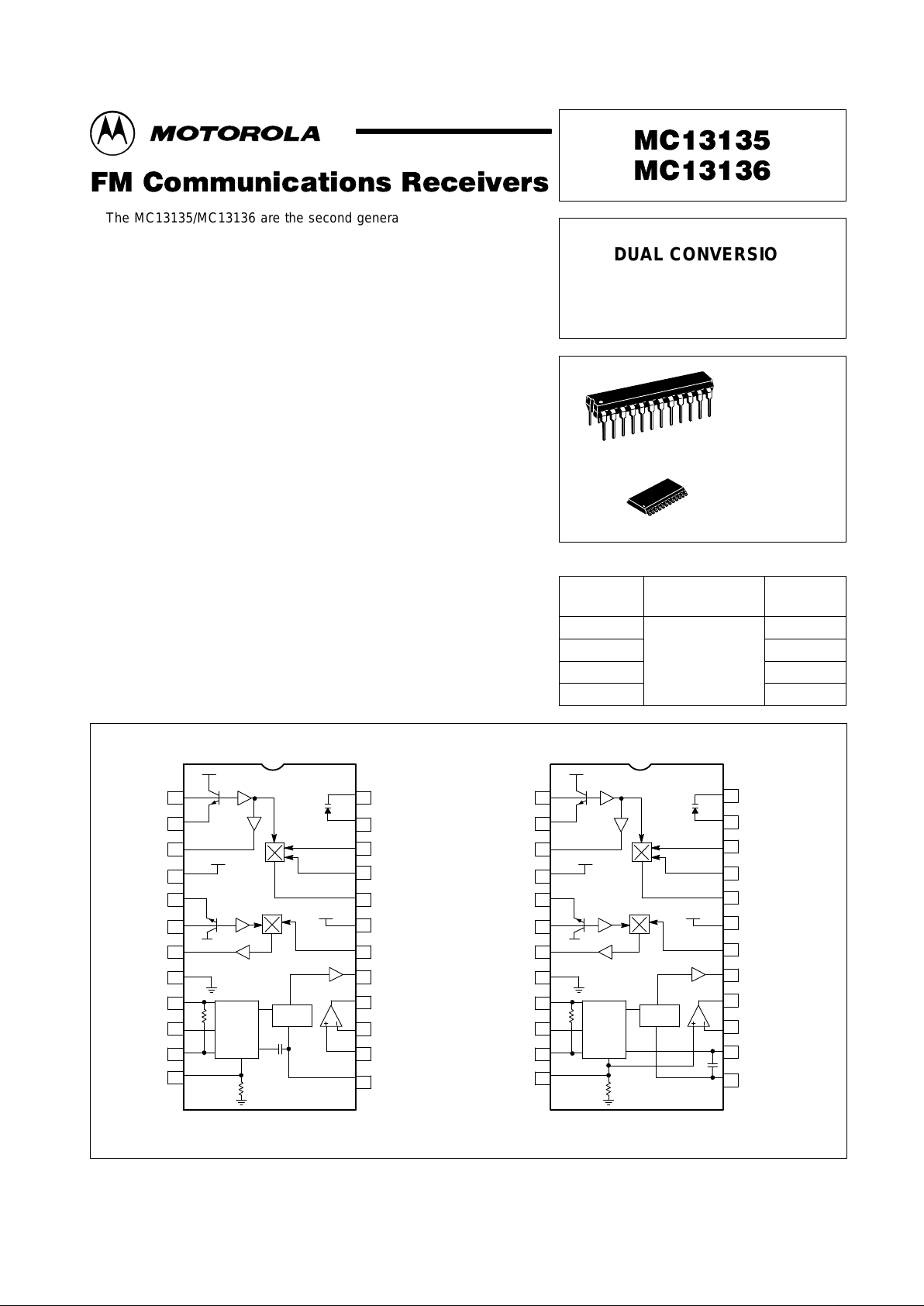
MC13135 MC13136
PIN CONNECTIONS
Each device contains 142 active transistors.
Motorola, Inc. 1996 Rev 3
MC13135 MC13136
2
MOTOROLA ANALOG IC DEVICE DATA
MAXIMUM RATINGS
Rating Pin Symbol Value Unit
Power Supply Voltage 4, 19 VCC (max) 6.5 Vdc
RF Input Voltage 22 RF
in
1.0 Vrms
Junction Temperature – T
J
+150 °C
Storage Temperature Range – T
stg
– 65 to +150 °C
RECOMMENDED OPERATING CONDITIONS
Rating Pin Symbol Value Unit
Power Supply Voltage 4, 19 V
CC
2.0 to 6.0 Vdc
Maximum 1st IF – f
IF1
21 MHz
Maximum 2nd IF – f
IF2
3.0 MHz
Ambient Temperature Range – T
A
– 40 to + 85 °C
ELECTRICAL CHARACTERISTICS (T
A
= 25°C, VCC = 4.0 Vdc, fo = 49.7 MHz, f
MOD
= 1.0 kHz, Deviation = ±3.0 kHz, f
1st LO
= 39 MHz, f
2nd
LO = 10.245 MHz, IF1 = 10.7 MHz, IF2 = 455 kHz, unless otherwise noted. All measurements performed in the test circuit of Figure 1.)
Characteristic
Condition Symbol Min Typ Max Unit
Total Drain Current No Input Signal I
CC
– 4.0 6.0 mAdc
Sensitivity (Input for 12 dB SINAD) Matched Input V
SIN
– 1.0 – µVrms
Recovered Audio VRF = 1.0 mV AF
O
mVrms
MC13135 170 220 300
MC13136 215 265 365
Limiter Output Level V
LIM
mVrms
(Pin 14, MC13136) – 130 –
1st Mixer Conversion Gain VRF = – 40 dBm MX
gain1
– 12 – dB
2nd Mixer Conversion Gain VRF = – 40 dBm MX
gain2
– 13 – dB
First LO Buffered Output – V
LO
– 100 – mVrms
Total Harmonic Distortion VRF = – 30 dBm THD – 1.2 3.0 %
Demodulator Bandwidth – BW – 50 – kHz
RSSI Dynamic Range – RSSI – 70 – dB
First Mixer 3rd Order Intercept TOI
Mix1
dBm
(Input) Matched – –17 –
Unmatched – –11 –
Second Mixer 3rd Order Matched TOI
Mix2
dBm
Intercept (RF Input) Input – –27 –
First LO Buffer Output Resistance – R
LO
– – – Ω
First Mixer Parallel Input Resistance – R – 722 – Ω
First Mixer Parallel Input Capacitance – C – 3.3 – pF
First Mixer Output Impedance – ZO – 330 – Ω
Second Mixer Input Impedance – Z
I
– 4.0 – kΩ
Second Mixer Output Impedance – ZO – 1.8 – kΩ
Detector Output Impedance – ZO – 25 – Ω
MC13135 MC13136
3
MOTOROLA ANALOG IC DEVICE DATA
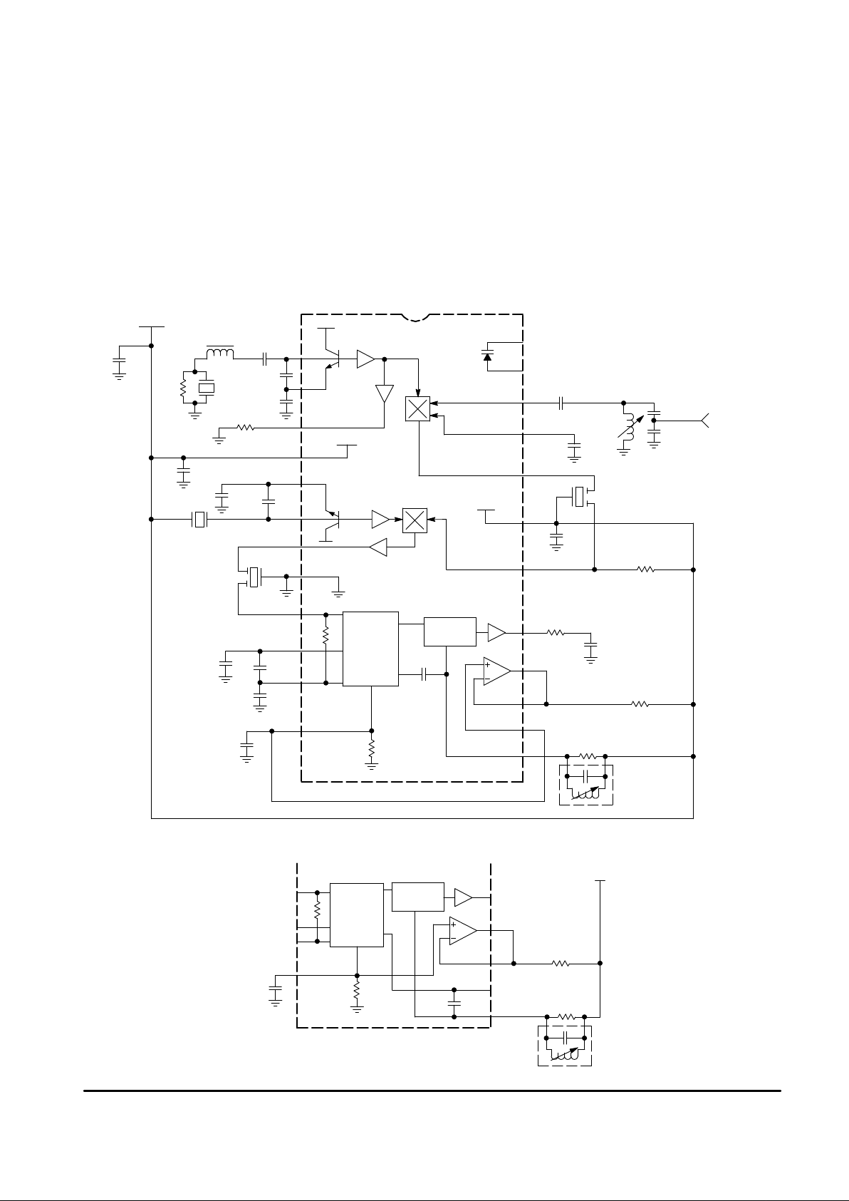
TEST CIRCUIT INFORMA TION
Although the MC13136 can be operated with a ceramic
discriminator, the recovered audio measurements for both
the MC13135 and MC13136 are made with an LC quadrature
detector. The typical recovered audio will depend on the
external circuit; either the Q of the quad coil, or the RC
matching network for the ceramic discriminator. On the
MC13136, an external capacitor between Pins 13 and 14 can
be used with a quad coil for slightly higher recovered audio.
See Figures 10 through 13 for additional information.
Since adding a matching circuit to the RF input increases
the signal level to the mixer, the third order intercept (TOI)
point is better with an unmatched input (50 Ω from Pin 21 to
Pin 22). Typical values for both have been included in the
Electrical Characterization Table. TOI measurements were
taken at the pins with a high impedance probe/spectrum
analyzer system. The first mixer input impedance was
measured at the pin with a network analyzer.
Figure 1.
V
CC
39 k
455 kHz
Quad Coil
39 k
0.1
12
16
15
14
13
AF
Limiter
Demod
Figure 1b. MC13136 Quad Detector Test Circuit
24
0.2 µH
RF
Input
62 pF
0.001
23
22
21
20
19
18
180 p
0.01
0.1
360
Ceramic
Filter
10.7 MHz
455 kHz
Quad
Coil
39 k
39 k
0.1
8.2 k
17
16
15
14
13
12
0.1
0.01
3
2
1
4
5
6
7
8
9
10
11
0.1
0.1
0.1
Ceramic
Filter
455 kHz
10.245
MHz Xtal
39.0
MHz
Xtal
20 p
5.0 p
50 p
5.0 k
120 p
0.1
V
CC
0.1
1.0 k
0.84
µ
H
AF
VCC2
2nd LO
VCC1
1st LO
Varicap
Limiter
Demod
Figure 1a. MC13135 Test Circuit
MC13135 MC13136
4
MOTOROLA ANALOG IC DEVICE DATA
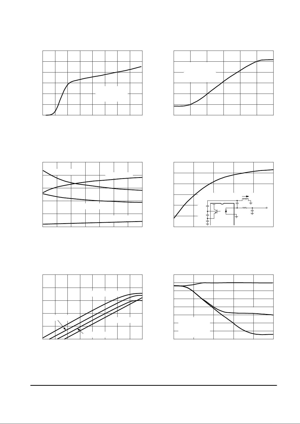
N
S+N, N, AND AMR (dB)
10
–130
RFin, RF INPUT (dBm)
f, FREQUENCY (MHz)
48.0
1.0
VB, VARACTOR BIAS VOLTAGE (Vdc)
RSSI OUTPUT (mVdc, Pin 12)
1400
–140
RF INPUT (dBm)
POWER (dBm)
30
–100
RFin, RF INPUT (dBm)
C
P
, EQUIVALENT PARALLEL CAPACITANCE (pF)
25
0.5
VB, VARACTOR BIAS VOLTAGE, V
Pin24
to V
Pin 23
(Vdc)
Figure 2. Supply Current versus Supply Voltage Figure 3. RSSI Output versus RF Input
Figure 4. Varactor Capacitance, Resistance
versus Bias Voltage
Figure 5. Oscillator Frequency
versus Varactor Bias
I
CC
, SUPPLY CURRENT (mA)
Figure 6. Signal Levels versus RF Input
6.0
0
VCC, SUPPLY VOLTAGE (V)
Figure 7. Signal + Noise, Noise, and
AM Rejection versus Input Power
RFin = 49.7 MHz
f
MOD
= 1.0 kHz
f
DEV
=
±
3.0 kHz
5.0
4.0
3.0
2.0
1.0
0
1.0 2.0 3.0 4.0 5.0 6.0 7.0 8.0
VCC = 4.0 V
RFin = 49.67 MHz
f
MOD
= 1.0 kHz
f
DEV
=
±
3.0 kHz
1200
1000
800
600
400
200
–120 –100 – 80 – 60 – 40 – 20
CP, f = 150 MHz
20
15
10
5.0
0
1.0 1.5 2.0 2.5 3.0 3.5 4.0
10
8.0
6.0
4.0
2.0
0
R
P
, EQUIVALENT PARALLEL RESISTANCE (k )
Ω
47.5
47.0
46.5
46.0
45.5
45.0
RP, f = 50 MHz
CP, f = 50 MHz
RP, f = 150 MHz
2.0 3.0 4.0 5.0 6.0
–90 –80 –70 –60 –50 –40 –30 –20
10
–10
–30
–50
–70
First Mixer Output
First Mixer Input
–110 – 90 – 70 – 50 – 30
0
–10
–20
–30
–40
–50
–60
–70
S + N
S + N 30% AM
VCC = 4.0 Vdc
RFin = 49.67 MHz
f
MOD
= 1.0 kHz
f
DEV
=
±
3.0 kHz
5.0 p
0.61
µ
H
1st LO
Varicap
500 p
500 p
1.0 M
Ω
0.2 µF
V
B
24
23
2
1
27 p
Second Mixer Output
Second Mixer Input
MC13135 MC13136
5
MOTOROLA ANALOG IC DEVICE DATA
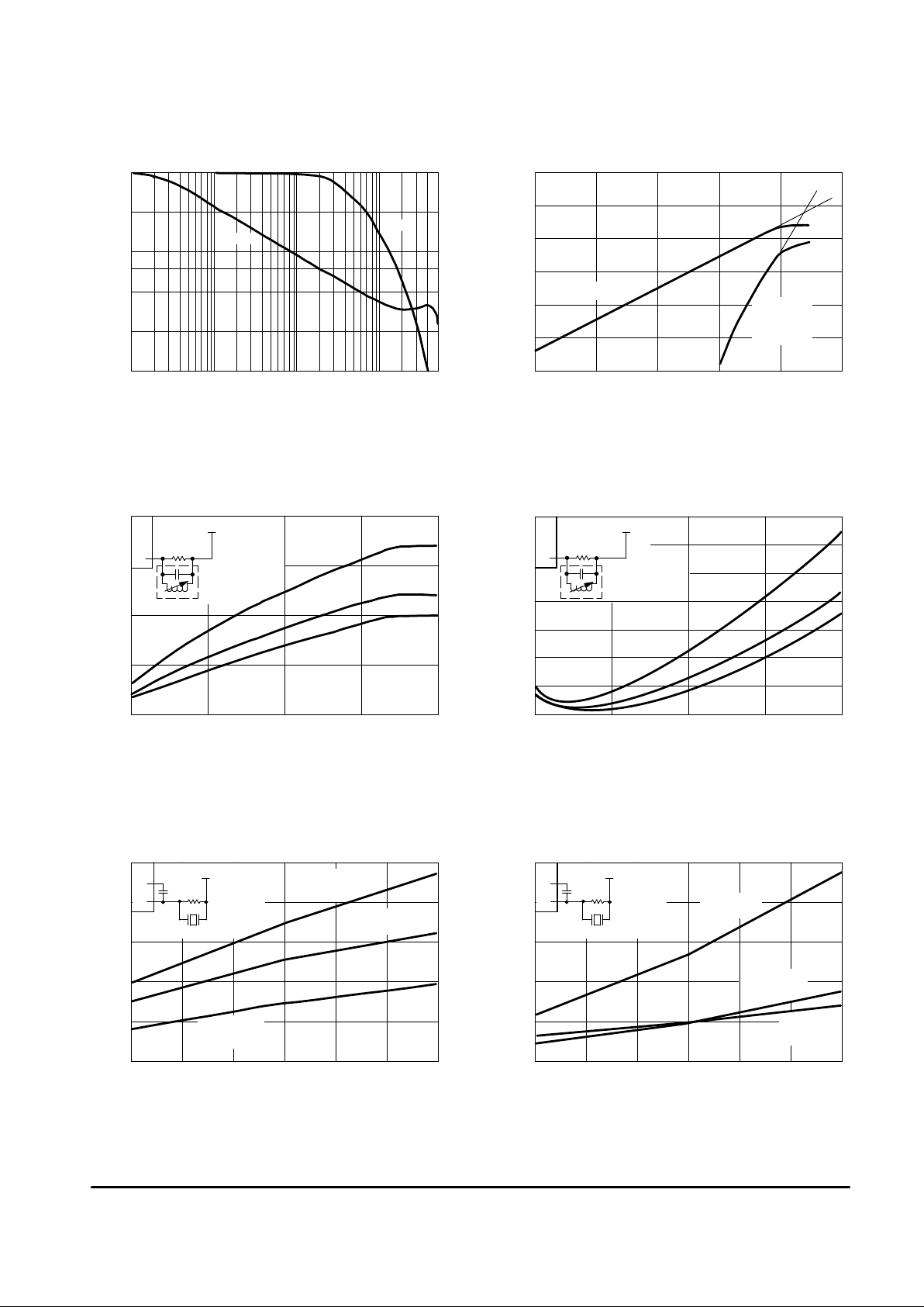
RA, RECOVERED AUDIO (mV )
pp
RA, RECOVERED AUDIO (mV )
, EXCESS PHASE (DEGREES)
φ
f
DEV
, DEVIATION (kHz)
THD, TOT AL HARMONIC DISTORTION (%)
8.0
f
DEV
, DEVIATION (kHz)
MIXER OUTPUT (dB)
20
–100
RF INPUT (dBm)
1000
±
3.0
2000
±
1.0
f
DEV
, DEVIATION (kHz)
Figure 8. Op Amp Gain and Phase
versus Frequency
Figure 9. First Mixer Third Order Intermodulation
(Unmatched Input)
Figure 10. Recovered Audio versus
Deviation for MC13135
Figure 11. Distortion versus
Deviation for MC13135
A
V
, GAIN (dB)
Figure 12. Recovered Audio versus
Deviation for MC13136
50
10 k
f, FREQUENCY (Hz)
Figure 13. Distortion versus
Deviation for MC13136
30
10
–10
–50
100 k 1.0 M 10 M
3rd Order
Intermod
Products
0
–20
–40
–60
–80
–100
– 80 –60 –40 – 20 0
1500
1000
1.0
R = 68 k
Ω
800
600
400
200
0
–30
80
120
160
200
280
240
Phase
Gain
Desired Products
±
3.0
±
5.0
±
7.0
±
9.0
pp
R = 47 k
Ω
R = 39 k
Ω
±
1.0
±
3.0
±
5.0
±
7.0
±
9.0
7.0
6.0
5.0
4.0
THD, TOT AL HARMONIC DISTORTION (%)
R = 68 k
Ω
R = 47 k
Ω
±
4.0
±
5.0
±
6.0
±
7.0
±
8.0
±
9.0
R =
∞
C = 660 pF
10
8.0
6.0
4.0
2.0
0
f
DEV
, DEVIATION (kHz)
±
3.0
±
4.0
±
5.0
±
6.0
±
7.0
±
8.0
±
9.0
R = 2.7 k
Ω
C = 270 pF
R = 2.7 k
Ω
C = 270 pF
R = 1.2 k
Ω
C = 100 pF
R
13
V
CC
455 kHz
Quad Coil
T oko 7MC–8128Z
500
0
3.0
2.0
R = 39 k
Ω
R
13
V
CC
muRata
455 kHz
Resonator
CDB455C34
R
14
13
C
V
CC
muRata
455 kHz
Resonator
CDB455C34
R
14
13
C
V
CC
R = 1.2 k
Ω
C = 100 pF
455 kHz
Quad Coil
T oko 7MC–8128Z
R =
∞
C = 660 pF
0
 Loading...