

Motorola MC13111AFTA, MC13111BFB, MC13111BFTA, MC13110AFB, MC13110AFTA Datasheet
...
Order this document by MC13110A/D
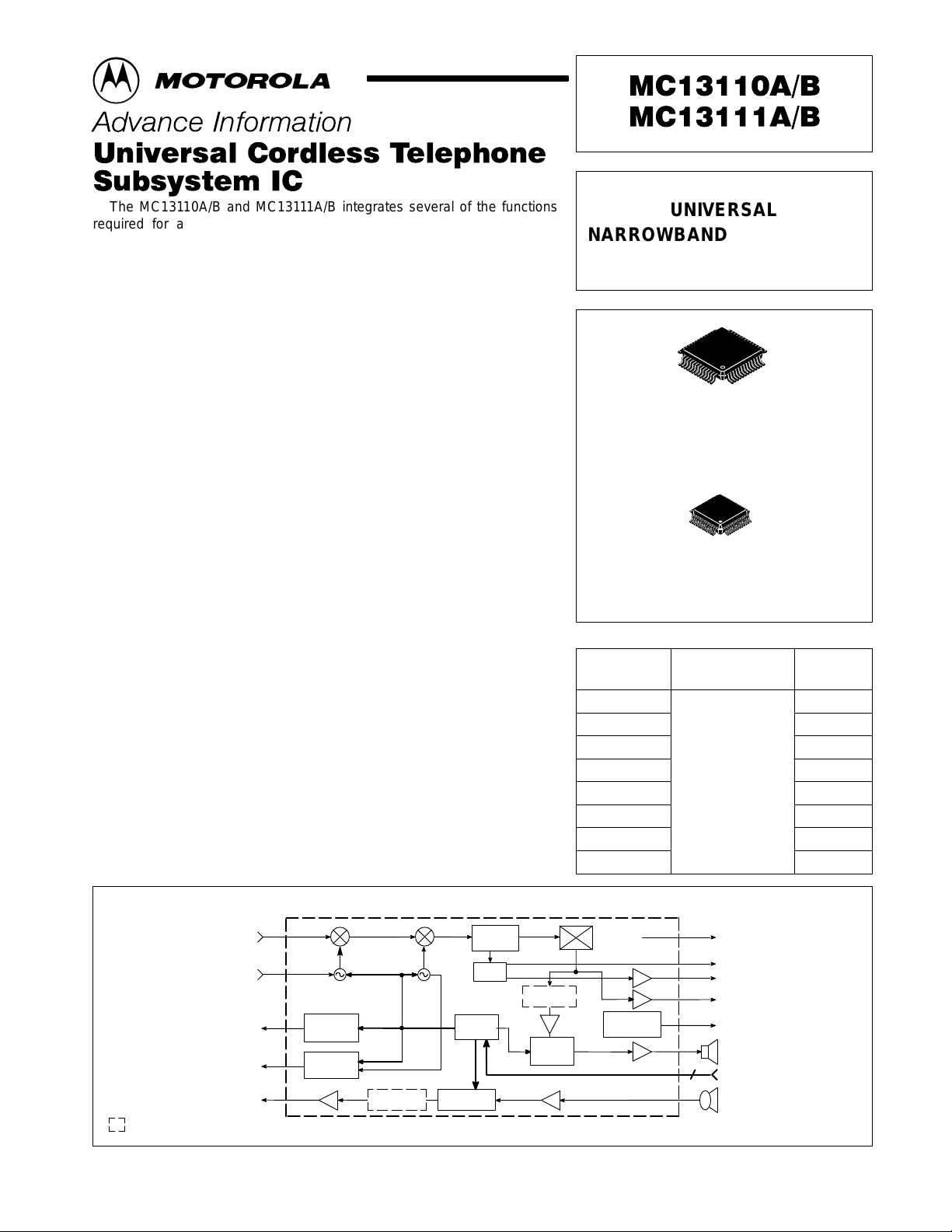
The MC13110A/B and MC13111A/B integrates several of the functions
required for a cordless telephone into a single integrated circuit. This
significantly reduces component count, board space requirements, external
adjustments, and lowers overall costs. It is designed for use in both the
handset and the base.
• MC13110A and MC13111A: Fully Programmable in all Power Modes
• MC13110B and MC13111B: MPU Clk Out and Second Local Oscillator
are “Always On”. There is No Inactive Mode
• Dual Conversion FM Receiver
– Complete Dual Conversion Receiver – Antenna Input to Audio Out
80 MHz Maximum Carrier Frequency
– RSSI Output
– Carrier Detect Output with Programmable Threshold
– Comparator for Data Recovery
– Operates with Either a Quad Coil or Ceramic Discriminator
• Compander
– Expander Includes Mute, Digital Volume Control, Speaker Driver,
Programmable Low Pass Filter, and Gain Block
– Compressor Includes Mute, Programmable Low Pass Filter, Limiter,
and Gain Block
• MC13110A/B only: Frequency Inversion Scrambler
– Function Controlled via MPU Interface
– Programmable Carrier Modulation Frequency
• Dual Universal Programmable PLL
– Supports New 25 Channel U.S. Standard with No External Switches
– Universal Design for Domestic and Foreign Cordless Telephone
Standards
– Digitally Controlled V ia a Serial Interface Port
– Receive Side Includes 1st LO VCO, Phase Detector, and 14–Bit
Programmable Counter and 2nd LO with 12–Bit Counter
– Transmit Section Contains Phase Detector and 14–Bit Counter
– MPU Clock Outputs Eliminates Need for MPU Crystal
• Low Battery Detect
– Provides Two Levels of Monitoring with Separate Outputs
– Separate, Adjustable Trip Points
• 2.7 to 5.5 V Operation (15 µA Current Consumption in Inactive Mode)
• AN1575: Refer to this Application Note for a List of the “Worldwide
Cordless Telephone Frequencies
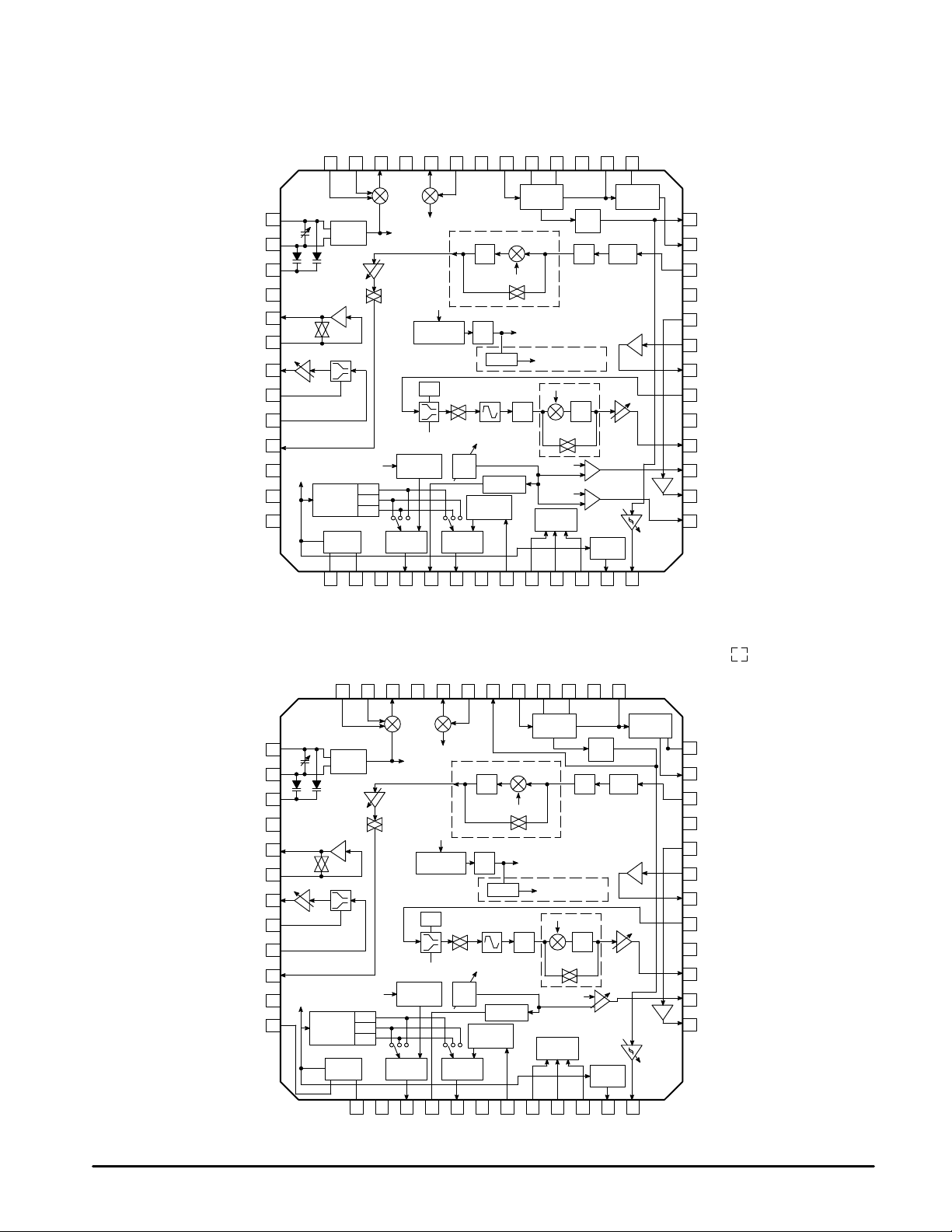
Simplified Block Diagram
UNIVERSAL
NARROWBAND FM RECEIVER
INTEGRATED CIRCUIT
52
1
FB SUFFIX
PLASTIC PACKAGE
CASE 848B
(QFP–52)
48 1
FTA SUFFIX
PLASTIC PACKAGE
CASE 932
(LQFP–48)
ORDERING INFORMATION
Tested Operating
Device
MC13110AFB
MC131 10AFTA
MC131 10BFB QFP–52
MC131 10BFTA LQFP–48
MC13111AFB
MC13111AFTA
MC13111BFB
MC13111BFTA
Temperature Range
TA = – 40° to +85°C
Package
QFP–52
LQFP–48
QFP–52
LQFP–48
QFP–52
LQFP–48
Rx In
Rx PD In
Rx PD Out
Tx PD Out
NOTE:
= MC13110A/B Only
This document contains information on a new product. Specifications and information herein
are subject to change without notice.
MOTOROLA ANALOG IC DEVICE DATA
Tx Out
1st
Mixer
1st LO 2nd LO
Rx Phase
Detector
Tx Phase
Detector
Scrambler
This device contains 8262 active transistors.
Limiting IF
2nd
Mixer
µ
P Serial
Interface
Compressor
Amplifier
RSSI
Scrambler
Expander
2nd LO
Detector
Low Battery
Detect
Motorola, Inc. 1997 Rev 0
MPU Clock Out
RSSI
Carrier Detect Out
Data Out
Low Battery
Indicator
Rx Out
SPI
Tx In
1
MC13110A/B MC13111A/B
PIN CONNECTIONS
QFP–52
2
In
Mix
39
1
1
In
1
Mix
38
Out
Mix
37
1
Gnd RF
36
Out
Mix
35
In
2
2
Mix
34
Lim In
SGnd RF
32
33
Lim C1
31
Lim C2
30
RF
CC
V
29
Lim Out
28
Q Coil
27
In
LO
1
Out
LO
1
Ctrl
V
cap
Gnd Audio
SA Out
SA In
E Out
E
cap
E In
Scr Out
Ref
2
Ref
1
VB
40
41
42
43
44
45
46
47
48
49
50
51
52
Speaker
Mute
Vol
Control
2nd LO
1st Mix 2nd Mix
1st LO
VCO
1st LO
Rx Gain
Adjust
In
Mix
36
1
1
1st LO
÷
25
÷
4
÷
1
2
Out
2
LO
35
R
x
Mute
Compressor
Rx Phase
Detect
3
Vag
2
In
1
Mix
34
Speaker
Amp
Expander
12 b Prog
Ref Ctr
2nd LO
10.240
1
InLO
2
2nd LO
14 b Prog
Rx Ctr
4
PD
x
R
Out
1
Mix
2nd LO
6 b Prog
SC Clk Ctr
ALC
Mute
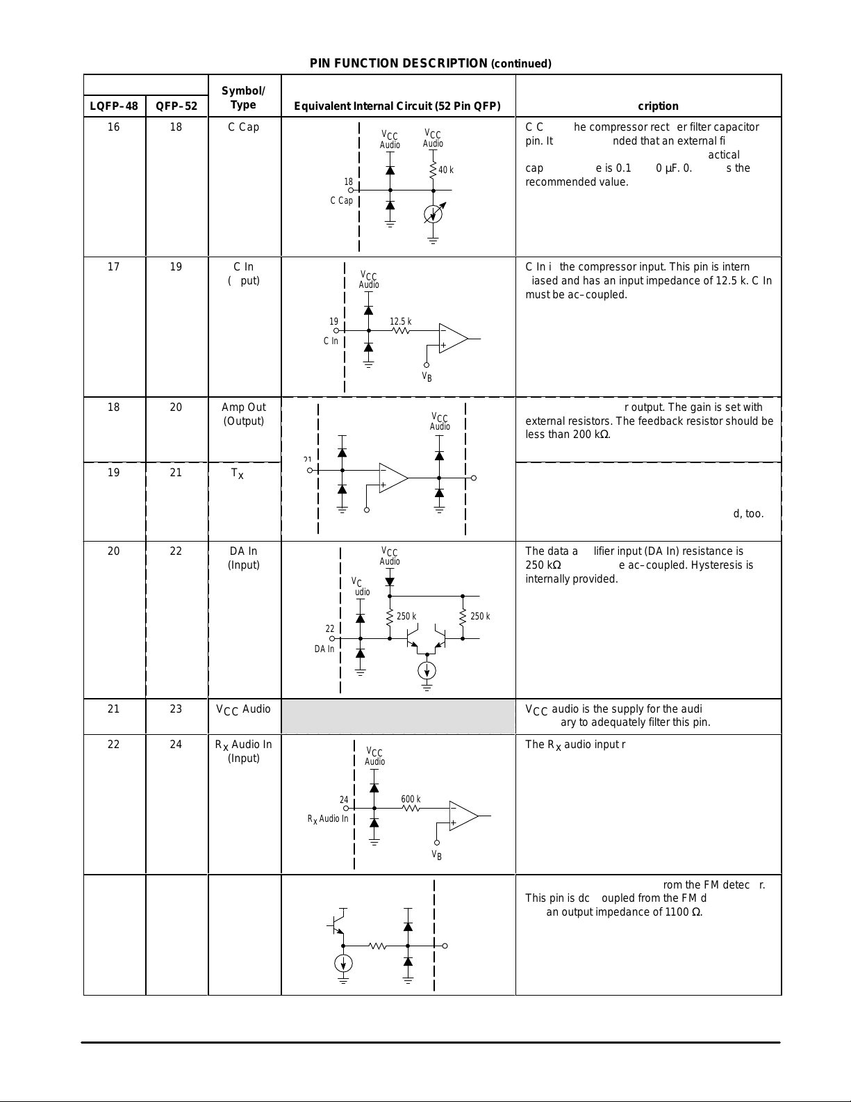
C Cap
Tx Phase
5
ref
PLL V
Out
2
Gnd RF
Mix
32
33
Scrambler
LPF
4.129 kHz
Bypass
÷
2
T
x
Limiter
VB
V
ref
Reg 2.5 V
14 b Prog
Tx Ctr
Detect
7
6
PD
x
T
Gnd PLL
LQFP–48
In
2
Mix
31
÷
40
RSSI
30
IF Amp/
Limiter
SC Filter
Clock
Scrambler
Modulating Clock
LPF
µ
9
8
Data
VCO
x
T
Lim In
29
4.129 kHz
Bypass
Ref
Ref
P Serial
Interface
10
EN
Lim C1
28
RSSI
LPF AALPF
Mic Amp
LPF
2
Low Battery
Detect
1
Prog
Clk Ctr
11
Clk
RF
CC
V
Lim C2
26
27
Detector
Tx Gain
Adjust
12
Clk Out
Lim Out
25
Data
Amp
Carrier
Detect
13
CD Out
26
25
24
23
22
21
20
19
18
17
16
15
14
RSSI
Det Out
R
Audio In
x
V
Audio
CC
DA In
T
In
x
Amp Out
C In
C Cap
T
Out
x
BD2 Out
DA Out
BD1 Out
NOTE:
= MC13110A/B Only
LO
In
1
LO
Out
1
Ctrl
V
cap
Gnd Audio
SA Out
SA In
E Out
E
cap
E In
Scr Out
VB
LO
In
2
37
38
39
40
41
42
43
44
45
46
47
48
Speaker
Mute
Vol
Control
2nd LO
1st LO
VCO
Speaker
Amp
Expander
12 b Prog
Ref Ctr
2nd LO
10.240
1st Mix 2nd Mix
2nd LO
1st LO
Rx Gain
Adjust
R
x
Mute
2nd LO
6 b Prog
SC Clk Ctr
T
ALC
Mute
Compressor
C Cap
÷
1
OutLO
14 b Prog
Rx Ctr
25
÷
4
÷
1
Rx Phase
Detect
2
Vag
2
Tx Phase
Detect
4
3
ref
PD
x
R
PLL V
1st LO
Scrambler
LPF
4.129 kHz
Bypass
÷
2
x
Limiter
VB
V
ref
14 b Prog
Tx Ctr
6
5
PD
x
T
Gnd PLL
÷
40
LPF
Reg 2.5 V
7
VCO
x
T
IF Amp/
Limiter
SC Filter
Clock
Scrambler
Modulating Clock
4.129 kHz
Bypass
VCC Audio
µ
P Serial
Interface
9
8
EN
Data
RSSI
LPF AALPF
Mic Amp
Tx Gain
Adjust
LPF
Programmable
Low Battery
Detect
Prog
Clk Ctr
11
10
Clk
Clk Out
Detector
Data
Amp
Carrier
Detect
12
CD Out
24
23
22
21
20
19
18
17
16
15
14
13
Q Coil
Det Out
R
Audio In
x
V
Audio
CC
DA In
T
In
x
Amp Out
C In
C Cap
T
Out
x
BD Out
DA Out
2
MOTOROLA ANALOG IC DEVICE DATA
MC13110A/B MC13111A/B
БББББ
БББББ
MAXIMUM RATINGS
Characteristic Symbol Value Unit
Power Supply Voltage
Junction Temperature
Maximum Power Dissipation, TA = 25°C P
NOTES: 1. Devices should not be operated at these limits. The “Recommended Operating Conditions”
provide for actual device operation.
2.ESD data available upon request.
RECOMMENDED OPERATING CONDITIONS
Characteristic Symbol Min Typ Max Unit
Supply Voltage V
Operating Ambient Temperature T
Input Voltage Low (Data, Clk, EN) V
Input Voltage High (Data, Clk, EN) V
Bandgap Reference Voltage V
NOTE: 3.All limits are not necessarily functional concurrently.
V
CC
T
J
D
CC
A
IL
IH
B
–0.5 to +6.0
–65 to +150
70 mW
2.7 3.6 5.5 Vdc
–40 – 85 °C
– – 0.3 V
PLL V
0.3
ref
–
– – V
– 1.5 – V
Vdc
°C
DC ELECTRICAL CHARACTERISTICS (V
= 3.6 V, TA = 25°C, unless otherwise specified, IP3 = 0;
CC
Test Circuit Figure 1.)
Characteristic
Symbol Figure Min Typ Max Unit
Static Current 1
Active Mode ACT I
Receive Mode Rx I
Standby Mode STD I
Inactive Mode [Note 4] INACT I
Current Increase When IP3 = 1
(Active and Receive Modes)
NOTE: 4.MC13110B/MC13111B versions have no inactive mode.
I
CC
CC
CC
CC
IP3
5.5 8.5 10.5 mA
3.1 4.1 5.3 mA
– 465 560 µA
– 15 30 µA
1 – 1.4 1.8 mA
MOTOROLA ANALOG IC DEVICE DATA
3
MC13110A/B MC13111A/B
ELECTRICAL CHARACTERISTICS (V
Test Circuit Figure 1.)
Characteristic
FM RECEIVER (fRF = 46.77 MHz [USA Ch 21], f
Input Sensitivity (for 12 dB SINAD at Det Out
Using C–Message Weighting Filter)
50 Ω T ermination, Generator Referred
Single–Ended, Matched Input, Generator
Referred
Differential, Matched Input, Generator Referred –
First and Second Mixer Voltage Gain Total
(Vin = 1.0 mVrms, with CF1 and CF2 Load)
Isolation of First Mixer Output and Second Mixer
Input (Vin = 1.0 mVrms, with CFI Removed)
Total Harmonic Distortion (Vin = 3.16 mVrms) 1 Mix
Recovered Audio (Vin = 3.16 mVrms) 1 Mix
AM Rejection Ratio (Vin = 3.16 mVrms, 30% AM,
@ 1.0 kHz)
Signal to Noise Ratio (Vin = 3.16 mVrms,
No Modulation)
FIRST MIXER (No Modulation, fin = USA Ch21, 46.77 MHz, 50 Ω T ermination at Inputs)
Input Impedance
Single–Ended
Differential 16 Mix
Output Impedance 14 – Mix1 Out RP1 Out
Voltage Conversion Gain
(Vin = 1.0 mVrms, with CF1 Filter as Load)
1.0 dB Voltage Compression Level (Input Referred)
IP3 Bit Set to 0
IP3 Bit Set to 1 20, 21 –
Third Order Intercept (Input Referred) [Note 5]
IP3 Bit Set to 0
IP3 Bit Set to 1 20, 21 –
–3.0 dB IF Bandwidth 22 Mix1 In
NOTE: 5.Third order intercept calculated for input levels 10 dB below 1.0 dB compression point.
= 3.6 V, VB = 1.5 V, TA = 25°C, Active or Rx Mode, unless otherwise specified;
CC
Figure
= ±3.0 kHz, f
dev
68, 69 Mix
1 Mix
– Mix
1 Mix
– Mix
16
17, 18 Mix
19, 21
19, 21
Input
Pin
mod
In1/In
In1 or In
In1 or In
In1 or In
In1 or In
In1 or In
In1 or In
–
In1 or In
Mix
In1 or In
Mix
In1 or In
or In
Measure
Pin
= 1.0 kHz, V
1
1
1
1
1
1
1
1
1
1
Det Out V
2
Mix2 Out MX
2
Mix2 In Mix–Iso – 60 – dB
2
Det Out THD – 1.4 2.0 %
2
Det Out AFO 80 112 150 mVrms
2
Det Out AMR 30 48 – dB
2
Det Out SNR – 48 – dB
2
Mix
In1 or In
In1/In
Mix1 Out MX
2
Mix1 Out VO Mix
2
Mix1 Out TOI
2
Mix1 Out Mix1 BW – 13 – MHz
1
2
Symbol Min Typ Max Unit
= 1.2 V)
cap ctrl
SIN
gainT
1
R
2
PS1
C
PS1
1
R
2
PD1
C
PD1
CP1 Out
gain1
1 dB
mix1
1
µVrms
–
–
–
–
–
24 29 – dB
–
–
–
–
–
–
– 12 – dB
–
–
–
–
–
–
2.2
–100
0.4
–115
0.4
–115
1.6
3.7
1.6
1.8
300
3.7
20
–21
56
–12
64
–11
178
–2.0
dBm
–
–
–
–
–
–
kΩ
–
–
–
–
–
–
–
–
–
–
–
–
–
–
pF
pF
mVrms
dBm
mVrms
dBm
Ω
4
MOTOROLA ANALOG IC DEVICE DATA
MC13110A/B MC13111A/B
ELECTRICAL CHARACTERISTICS (continued) (V
Test Circuit Figure 1.)
Characteristic UnitMaxTypMinSymbol
SECOND MIXER (No Modulation, fin = 10.7 MHz, 50 Ω T ermination at Inputs)
Input Impedance 24 Mix2 In Mix2 In RP2 In
Output Impedance 24 – Mix2 Out RP2 Out
Voltage Conversion Gain
(Vin = 1.0 mVrms, with CF2 Filter as Load)
1.0 dB Voltage Compression Level (Input Referred)
IP3 Bit Set 0
IP3 Bit Set 1 29, 30 –
Third Order Intercept (Input Referred) [Note 6]
IP3 Bit Set 0
IP3 Bit Set 1 29, 30 –
–3.0 dB IF Bandwidth 31 Mix2 In Mix2 Out Mix2 BW – 2.5 – MHz
LIMITER/DEMODULA TOR (fin = 455 kHz, f
Input Impedance 49 Lim In Lim In R
Detector Output Impedance – – Det Out R
IF –ā3.0 dB Limiting Sensitivity
Demodulator Bandwidth – Lim In Det Out BW – 20 – kHz
RSSI/CARRIER DETECT (No Modulation)
RSSI Output Dynamic Range 56 Mix1 In RSSI RSSI – 80 – dB
DC Voltage Range 56 Mix1 In RSSI DC RSSI – 0.2 to
Carrier Detect Threshold
CD Threshold Adjust = (10100)
(Threshold Relative to Mix1 In Level)
Hysteresis, CD = (10100)
(Threshold Relative to Mix1 In Level)
Output High Voltage
CD = (00000), RSSI = 0.2 V
Output Low Voltage
CD = (11111), RSSI = 0.9 V
Carrier Detect Threshold Adjustment Range
(Programmable through MPU Interface)
Carrier Detect Threshold – Number of
Programmable Levels
NOTE: 6.Third order intercept calculated for input levels 10 dB below 1.0 dB compression point.
= ±3.0 kHz, f
dev
= 3.6 V, VB = 1.5 V, TA = 25°C, Active or Rx Mode, unless otherwise specified;
CC
Input
Figure
26, 27 Mix2 In Mix2 Out MX
28, 30
28, 30
1 Lim In Det Out IF Sens – 71 100 µVrms
57 Mix1 In CD Out V
57 Mix1 In CD Out Hys – 2.0 – dB
1 RSSI CD Out V
1 RSSI CD Out V
126 – – V
126 – – V
Pin
Mix2 In Mix2 Out V
Mix2 In Mix2 Out TOI
= 1.0 kHz)
mod
Measure
Pin
CP2 In
CP2 Out
gain2
O
Mix
2
1 dB
mix2
PLim
C
PLim
O
T
OH
OL
T
Range
Tn
–
–
–
–
– 20 – dB
–
–
–
–
–
–
–
–
– 1.1 – kΩ
– 15 – µVrms
VCC –
0.1
– 0.02 0.4 V
– –20 to
– 32 – –
2.8
3.6
1.5
6.1
32
–17
45
–14
136
–4.3
158
–3.0
1.5
16
1.5
3.6 – V
11
–
–
–
–
–
–
–
–
–
–
–
–
–
–
– Vdc
– dB
kΩ
pF
kΩ
pF
mVrms
dBm
mVrms
dBm
kΩ
pF
MOTOROLA ANALOG IC DEVICE DATA
5
MC13110A/B MC13111A/B
pp
x
in
ELECTRICAL CHARACTERISTICS
Test Circuit Figure 1.)
Characteristic UnitMaxTypMinSymbol
Rx AUDIO PATH (fin = 1.0 kHz, Active Mode, scrambler bypassed)
Absolute Gain (Vin = –20 dBV) 1, 72 Rx Audio In SA Out G –4.0 0 4.0 dB
Gain Tracking
(Referenced to E Out for Vin = –20 dBV)
Vin = –30 dBV –21 –20 –19
Vin = –40 dBV –42 –40 –38
Total Harmonic Distortion (Vin = –20 dBV) 1, 76 Rx Audio In SA Out THD – 0.7 1.0 %
Maximum Input Voltage (VCC = 2.7 V) 76 Rx Audio In – – – –11.5 – dBV
Maximum Output Voltage (Increase input voltage
until output voltage THD = 5.0%, then measure
output voltage)
Input Impedance – Rx Audio In
Attack Time
E
= 0.5 µF, R
cap
Release Time
E
= 0.5 µF, R
cap
Compressor to Expander Crosstalk
Vin = –10 dBV, V(E
Rx Muting (∆ Gain)
Vin = –20 dBV, Rx Gain Adj = (01111)
Rx High Frequency Corner
Rx Path, V Rx Audio In = –20 dBV
Low Pass Filter Passband Ripple (Vin = –20 dBV) 1, 73 Rx Audio In Scr Out Ripple – 0.4 0.6 dB
Rx Gain Adjust Range (Programmable through
MPU Interface)
Rx Gain Adjust Steps – Number of
Programmable Levels
Audio Path Noise, C–Message Weighting
(Input AC–Grounded)
Volume Control Adjust Range 123 E In E Out Vcn
Volume Control – Number of Programmable
Levels
SPEAKER AMP/SP MUTE (Active Mode)
Maximum Output Swing
RL = No Load, Vin = 3.4 Vpp
RL = 130 Ω, Vin = 2.8 Vpp
RL = 620 Ω, Vin = 4.0 Vpp
Speaker Amp Muting
Vin = –20 dBV, RL = 130 Ω
= 40 k (See Appendix B)
filt
= 40 k (See Appendix B)
filt
= AC Gnd
In)
(continued) (VCC = 3.6 V, VB = 1.5 V, TA = 25°C, Active or Rx Mode, unless otherwise specified;
Input
Figure
1, 76 E In E Out G
1 E In E Out V
– E In E Out t
– E In E Out t
1 C In E Out C
1 Rx Audio In E Out M
1 Rx Audio In Scr Out Rx f
125 Rx Audio In Scr Out R
125 Rx Audio In Scr Out Rx n – 20 – dB
70 Rx Audio In Scr Out
123 E In E Out V
1, 79 SA In SA Out V
1 SA In SA Out M
Pin
E In
Measure
Pin
– Z
E Out
SA Out
t
Omax
in
a
r
T
e
ch
x
Range
EN –
Range
cn
Omax
sp
dB
–2.0 0 – dBV
– 600
– 7.5 –
– 3.0 – ms
– 13.5 – ms
– –90 –70 dB
– –84 –60 dB
3.779 3.879 3.979 kHz
– –9.0 to
–
– –14 to
– 16 – –
2.8
2.0
–
– –92 –60 dB
10
–85
<–95
<–95
16
3.2
2.6
3.4
– k Ω
– dB
–
dBV
–
– dB
–
–
–
Vpp
6
MOTOROLA ANALOG IC DEVICE DATA
MC13110A/B MC13111A/B
x
p
ELECTRICAL CHARACTERISTICS (continued) (V
Test Circuit Figure 1.)
Characteristic UnitMaxTypMinSymbol
DATA AMP COMPARATOR
Hysteresis 1 DA In DA Out Hys 30 42 50 mV
Threshold Voltage – DA In DA Out V
Input Impedance 1 – DA In Z
Output Impedance – – DA Out Z
Output High Voltage
Vin = VCC – 1.0 V, IOH = 0 mA
Output Low Voltage
Vin = VCC – 0.4 V, IOL = 0 mA
Maximum Frequency – DA In DA Out F
MIC AMP (fin = 1.0 kHz, External resistors set to gain of 1, Active Mode)
Open Loop Gain – Tx In Amp Out AVOL – 100,000 – V/V
Gain Bandwidth – Tx In Amp Out GBW – 100 – kHz
Maximum Output Swing (RL = 10 kΩ) – Tx In Amp Out V
Tx AUDIO PATH (fin = 1.0 kHz, Tx Gain Adj = (01111); ALC, Limiter, and Mutes Disabled; Active Mode, scrambler bypassed)
Absolute Gain (Vin = –10 dB V) 1, 83 Tx In Tx Out G –4.0 0 4.0 dB
Gain Tracking
(Referenced to Tx Out for Vin = –10 dBV)
Vin = –30 dBV
Vin = –40 dBV
Total Harmonic Distortion (Vin = –10 dBV) 1, 87 Tx In Tx Out THD – 0.8 1.8 %
Maximum Output Voltage (Increase input voltage
until output voltage THD = 5.0%, then measure
output voltage. Tx Gain Adjust = 8 dB)
Input Impedance – – C In Z
Attack Time (C
Appendix B))
Release Time (C
Appendix B))
Expander to Compressor Crosstalk (Vin = –20 dBV,
Speaker Amp No Load, V(C
Tx Muting (Vin – 10 dBV) 1 Tx In Tx Out M
ALC Output Level (ALC enabled)
Vin = –10 dBV
Vin = –2.5 dBV
ALC Slope (ALC enabled)
Vin = –10 dBv
Vin = –2.5 dBv
ALC Input Dynamic Range – C In Tx Out DR – –16 to
Limiter Output Level (Vin = –2.5 dBV,
Limiter enabled)
Tx High Frequency Corner [Note 7]
(VTx In = –10 dBV, Mic Amp = Unity Gain)
NOTE: 7.The filter specification is based on a 10.24 MHz 2nd LO, and a switched–capacitor (SC) filter counter divider ratio of 31. If other 2nd LO frequencies
= 0.5 µF, R
cap
= 0.5 µF, R
cap
and/or SC filter counter divider ratios are used, the filter corner frequency will be proportional to the resulting SC filter clock frequency.
= 40 k (See
filt
= 40 k (See
filt
= AC Gnd)
In)
= 3.6 V, VB = 1.5 V, TA = 25°C, Active or Rx Mode, unless otherwise specified;
CC
Input
Figure
1 DA In DA Out V
1 DA In DA Out V
1, 87 Tx In Tx Out G
1 Tx In Tx Out V
– C In Tx Out t
– C In Tx Out t
1 E In Tx Out C
1, 87,
90
1 Tx In
1 Tx In Tx Out V
1 Tx In Tx Out Tx f
Pin
Tx In Tx Out ALC
Measure
Pin
Tx Out
T
I
O
OH
OL
max
Omax
t
Omax
in
a
r
T
c
out
Slope
lim
– VCC –
200 250 280 kΩ
– 100 – kΩ
VCC –
0.1
– 0.1 0.4 V
– 10 – kHz
– 3.2 – Vpp
–11
–17
–2.0 0 – dBV
– 10 – kΩ
– 3.0 – ms
– 13.5 – ms
– –60 –40 dB
– –88 –60 dB
–15
–13
0.1 0.25 0.4 dB/dB
–10 –8.0 – dBV
3.6 3.7 3.8 kHz
c
0.7
3.6 – V
–10
–15
–13
–11
–2.5
– V
dB
–9.0
–13
dBV
–8.0
–6.0
– dBV
MOTOROLA ANALOG IC DEVICE DATA
7
MC13110A/B MC13111A/B
x
,
in
ELECTRICAL CHARACTERISTICS
Test Circuit Figure 1.)
Characteristic UnitMaxTypMinSymbol
Tx AUDIO PATH (fin = 1.0 kHz, Tx Gain Adj = (01111); ALC, Limiter, and Mutes Disabled; Active Mode, scrambler bypassed)
Low Pass Filter Passband Ripple (Vin = –10 dBV) 1, 84 Tx In Tx Out Ripple – 0.7 1.2 dB
Maximum Compressor Gain (Vin = –70 dBV) – C In Tx Out AV
Tx Gain Adjust Range (Programmable through
MPU Interface)
Tx Gain Adjust Steps – Number of Programmable
Levels
Rx AND Tx SCRAMBLER (2nd LO = 10.24 MHz, Tx Gain Adj = (01111), Rx Gain Adj = (01111), Volume Control = (0 dB Default Levels),
SCF Clock Divider = 31. Total is divide by 62 for SCF clock frequency of 165.16 kHz)
Rx High Frequency Corner (Note 8)
Rx Path, f = 479 Hz, V Rx Audio In = –20 dBV
Tx High Frequency Corner (Note 8)
Tx Path, f = 300 Hz, V Tx In = –10 dBV,
Mic Amp = Unity Gain
Absolute Gain
Rx: Vin = –20 dBV
Tx: Vin = –10 dBV, Limiter disabled
Pass Band Ripple
Rx + Tx Path – 1.0 µF from Tx Out to
Rx Audio In, fin = low corner frequency to
high corner frequency
Scrambler Modulation Frequency
Rx: 100 mV (–20 dBV)
Tx: 316 mV (–10 dBV)
Group Delay
Rx + Tx Path – 1.0 µF from Tx Out to
Rx Audio In, fin = 1.0 kHz
fin = low corner frequency to high corner
frequency
Carrier Breakthrough
Rx + Tx Path – 1.0 µF from Tx Out to
Rx Audio In
Baseband Breakthrough
Rx + Tx Path – 1.0 µF from Tx Out to
Rx Audio In,
fin = 1.0 kHz, f
LOW BATTERY DETECT
Average Threshold
Voltage Before Electronic Adjustment
(V
_Adj = (0111))
ref
Average Threshold
Voltage After Electronic Adjustment
(V
_Adj = (adjusted value))
ref
Hysteresis – Ref
Input Current (Vin = 1.0 and 2.0 V) 1 – Ref
Output High Voltage (Vin = 2.0 V) 1 Ref
NOTE: 8.The filter specification is based on a 10.24 MHz 2nd LO, and a switch–capacitor (SC) filter counter divider ratio of 31. If other 2nd LO frequencies
and/or SC filter counter divider ratios are used, the filter corner frequency will be proportional to the resulting SC filter clock frequency.
meas
= 3.192 kHz
(continued) (VCC = 3.6 V, VB = 1.5 V, TA = 25°C, Active or Rx Mode, unless otherwise specified;
Input
Figure
125 C In Tx Out Tx Range – –9.0 to
125 C In Tx Out Tx n – 20 – –
– Rx Audio In Scr Out Rx f
– Tx In Tx Out Tx f
–
–
– C In E Out Ripple – 1.9 2.5 dB
–
–
– C In E Out GD – 1.0 –
– C In E Out GD – 4.0 –
– C In E Out CBT – –60 – dB
– C In E Out BBT – –50 – dB
1, 131 Ref
1 Ref
Pin
Rx Audio In
Tx In
Rx Audio In
C In
Ref
Ref
Ref
Ref
Measure
Pin
max
ch
ch
E Out
Tx Out
E Out
Tx Out
BD1 Out
1
BD2 Out
2
BD1 Out
1
BD2 Out
2
BD1 Out
1
BD2 Out
2
1
Ref
2
BD1 Out
1
BD2 Out
2
AV
f
mod
VT
i
VT
f
Hys – 4.0 – mV
I
in
V
OH
– 23 – dB
10
3.55 3.65 3.75 kHz
3.829 3.879 3.929 kHz
–4.0
–4.0
4.119 4.129 4.139 kHz
1.38 1.48 1.58 V
1.475 1.5 1.525 V
–50 – 50 nA
VCC –
0.1
0.4
–1.0
3.6 – V
– dB
dB
4.0
4.0
ms
8
MOTOROLA ANALOG IC DEVICE DATA
MC13110A/B MC13111A/B
CC
ELECTRICAL CHARACTERISTICS (continued) (V
Test Circuit Figure 1.)
Characteristic UnitMaxTypMinSymbol
LOW BATTERY DETECT
Output Low Voltage (Vin = 1.0 V) 1 Ref
BATTERY DETECT INTERNAL THRESHOLD
After Electronic Adjustment of VB Voltage
BD Select = (111)
BD Select = (110) IBS
BD Select = (101) IBS
BD Select = (100) IBS
BD Select = (011) IBS
BD Select = (010) IBS
BD Select = (001) IBS
PLL PHASE DETECTOR
Output Source Current
(VPD = Gnd + 0.5 V to PLL V
Output Sink Current
(VPD = Gnd + 0.5 V to PLL V
PLL LOOP CHARACTERISTICS
Maximum 2nd LO Frequency
(No Crystal)
Maximum 2nd LO Frequency
(With Crystal)
Maximum Tx VCO (Input Frequency),
Vin = 200 mVpp
PLL VOLTAGE REGULATOR
Regulated Output Level (IL = 0 mA, after V
Adjustment)
Line Regulation (IL = 0 mA, VCC = 3.0 to 5.5 V) 1 VCC Audio PLL V
Load Regulation (IL = 1.0 mA) 1 VCC Audio PLL V
MICROPROCESSOR SERIAL INTERFACE
Input Current Low (Vin = 0.3 V, Standby Mode) 1 – Data,
Input Current High (Vin = 3.3 V, Standby Mode) 1 – Data,
Hysteresis Voltage – – Data,
Maximum Clock Frequency – Data,
Input Capacitance – Data,
EN to Clk Setup Time 106 – EN, Clk t
Data to Clk Setup Time 105 – Data, Clk t
Hold Time 105 – Data, Clk t
Recovery Time 106 – EN, Clk t
Input Pulse Width – – EN, Clk t
MPU Interface Power–Up Delay (90% of PLL V
to Data,Clk, EN)
– 0.5 V)
ref
– 0.5 V)
ref
ref
ref
= 3.6 V, VB = 1.5 V, TA = 25°C, Active or Rx Mode, unless otherwise specified;
CC
Input
Figure
1, 128 VCC Audio
– – Rx PD
– – Rx PD
– LO2 In – f
– – LO2 In
– – Tx VCO f
1 – PLL V
108 – – t
Pin
Ref
EN, Clk
Clk, EN
Measure
Pin
BD1 Out
1
BD2 Out
2
BD2 Out V
Tx PD
Tx PD
LO2 Out
txmax
ref
refVReg
V
ref
Clk, EN
Clk, EN
Clk, EN
– – – 2.0 – MHz
– C
V
suDC
puMPU
V
OL
IBS
7
6
5
4
3
2
1
I
OH
I
OL
2ext
f
2ext
V
O
Line – 11.8 40 mV
Reg
Load
I
IL
I
IH
hys
in
suEC
h
rec
w
– 0.2 0.4 V
3.381 3.455 3.529
3.298 3.370 3.442
3.217 3.287 3.357
3.134 3.202 3.270
2.970 3.034 3.098
2.886 2.948 3.010
2.802 2.862 2.922
– 1.0 – mA
– 1.0 – mA
– 12 – MHz
– 12 – MHz
– 80 – MHz
2.4 2.5 2.6 V
–20 –1.4 – mV
–5.0 0.4 – µA
– 1.6 5.0 µA
– 1.0 – V
– 8.0 – pF
– 200 – ns
– 100 – ns
– 90 – ns
– 90 – ns
– 100 – ns
– 100 – µs
MOTOROLA ANALOG IC DEVICE DATA
9
MC13110A/B MC13111A/B
2
L
22.1 k
CC
V
10
0.1
µ
10 F
0.1 0.1
2
CF
455 kHz
332
CC
To V
Figure 1. Production Test Circuit (52 Pin QFP)
1
CF
10.7 MHz
Audio In
x
R
1000
Det Out
15 k
0.01
0.1
27282930313233343536373839
Coil
Q
RF
2
1
2
In
Out
Out
1
In
1
Audio
CC
V
26
RSSI
Lim Out
CC
V
Lim C
Lim C
Lim In
SGnd RF
Mix
2
Mix
Gnd RF
1
Mix
1In2
Mix
Mix
1In1
LO
40
0.1
µ
10 F
25
Det Out
Out
LO
41
In
x
T
DA In
49.9 k
0.1
23
24
Audio
Audio In
CC
x
V
R
V Cap Ctrl
Gnd Audio
42
43
0.1
49.9 k
22
DA In
SA Out
44
Mic Amp Out
21
In
x
T
MC13110A/B
SA In
45
C In
0.1
20
C In
Amp Out
IC
MC13111A/B
E Out
E Cap
46
0.1
0.1
19
47
CCA
V
18
C Cap
E In
48
Out
x
T
F
µ
1.0
7.5 k
Out
2
Data Out
BD
CC
V
100 k
15
16
17
Out2Out1Out
x
T
DA Out
BD
BD
ref
2
1
Scr Out
Ref
Ref
V
51
50
49
µ
Out
1
BD
CC
V
Carrier
100 k
Detect Out
≥
Legend:
If 1, then capacitor value = pF
If <1, then capacitor value = F
100 k
14
Out
13121110987543216
CD
Clk Out
Clk
MPU Clock Output
VCO
x
T
0.1
µ
10 F
0.1
Out
In
B
VCO
PD
PD
2
2
EN
Data
x
T
Gnd PLL
x
T
PLL V
x
R
ag
V
LO
LO
0.01
52
NOTE: This schematic is only a partial representation of the actual production test circuit.
10
0.01
RF In
49.9 0.01
L3
33
110
µ
10 F
SA Out
49.9 k
0.1
SA In
49.9 k
CCA
V
0.1
0.1
E In
µ
7.5 k
1.0 F
E Out
µ
1.0 F
5.0 – 50 8.2
10.240 MHz
0.1
0.1
0.047
3.01 k
1.0 k
1.0 k
1.5 k22.1 k
ref1
V
Scr Out
ref2
V
32.4 k
0.1
Loop Filter
x
R
4700
MOTOROLA ANALOG IC DEVICE DATA
Pin
Symbol/
Á
Á
Á
Á
Á
Á
Á
Á
Á
Á
Á
Á
Á
Á
Á
Á
Á
Á
Á
Á
Á
Á
Á
Á
Á
Á
Á
Á
Á
Á
Á
Á
Á
Á
Á
Á
Á
Á
Á
Á
Á
Á
Á
Á
Á
Á
Á
Á
Á
Á
Á
Á
Á
Á
Á
Á
Á
Á
Á
Á
Á
Á
Á
Á
Á
Á
Á
Á
Á
Á
Á
Á
p
Á
Á
Á
Á
Á
Á
Á
Á
narrow pulses with a frequency equal to the
Á
Á
Á
Á
Á
Á
Á
Á
Á
Á
Á
Á
Á
Á
Á
Á
Á
Á
Á
Á
Á
Á
Á
Á
Á
Á
Á
Á
Á
Á
Á
Á
Á
Á
Á
Á
Á
Á
Á
Á
Á
Á
Á
Á
Á
Á
Á
Á
Á
Á
Á
Á
Á
Á
Á
Á
Á
Á
Á
Á
Á
Á
Á
Á
Á
Á
Á
Á
Á
Á
Á
Á
Á
Á
Á
LQFP–48
48
ÁÁ
1
ÁÁ
ÁÁ
ÁÁ
ÁÁ
ÁÁ
ÁÁ
ÁÁ
ÁÁ
ÁÁ
2
ÁÁ
ÁÁ
ÁÁ
ÁÁ
ÁÁ
ÁÁ
3
ÁÁ
ÁÁ
5
ÁÁ
ÁÁ
ÁÁ
4
ÁÁ
ÁÁ
ÁÁ
ÁÁ
ÁÁ
ÁÁ
ÁÁ
ÁÁ6ÁÁ7ÁÁÁ
7
ÁÁ
ÁÁ
ÁÁ
ÁÁ
ÁÁ
ÁÁ
ÁÁ
ÁÁ
ÁÁ
MOTOROLA ANALOG IC DEVICE DATA
QFP–52
1
ÁÁ
2
ÁÁ
ÁÁ
ÁÁ
ÁÁ
ÁÁ
ÁÁ
ÁÁ
ÁÁ
ÁÁ
3
ÁÁ
ÁÁ
ÁÁ
ÁÁ
ÁÁ
ÁÁ
4
ÁÁ
ÁÁ
6
ÁÁ
ÁÁ
ÁÁ
5
ÁÁ
ÁÁ
ÁÁ
ÁÁ
ÁÁ
ÁÁ
ÁÁ
8
ÁÁ
ÁÁ
ÁÁ
ÁÁ
ÁÁ
ÁÁ
ÁÁ
ÁÁ
ÁÁ
S
mbol/
Type
LO2 In
ÁÁÁ
LO2 Out
ÁÁÁ
ÁÁÁ
ÁÁÁ
ÁÁÁ
ÁÁÁ
ÁÁÁ
ÁÁÁ
ÁÁÁ
ÁÁÁ
V
ag
ÁÁÁ
ÁÁÁ
ÁÁÁ
ÁÁÁ
ÁÁÁ
ÁÁÁ
Rx PD
(Output)
ÁÁÁ
ÁÁÁ
Tx PD
(Output)
ÁÁÁ
ÁÁÁ
ÁÁÁ
PLL V
ref
ÁÁÁ
ÁÁÁ
ÁÁÁ
ÁÁÁ
ÁÁÁ
ÁÁÁ
ÁÁÁ
Gnd PLL
Tx VCO
ÁÁÁ
(Input)
ÁÁÁ
ÁÁÁ
ÁÁÁ
ÁÁÁ
ÁÁÁ
ÁÁÁ
ÁÁÁ
ÁÁÁ
MC13110A/B MC13111A/B
PIN FUNCTION DESCRIPTION
Equivalent Internal Circuit (52 Pin QFP)
PLL
V
ref
PLL
V
ref
100
3
V
ag
4, 6
Rx PD,
Tx PD
PLL
V
ref
PLL
V
ref
2
LO2
Out
100
LO
1
2
In
V
Audio
CC
PLL
V
PLL
V
ref
ref
30 k
PLL
V
ref
15
1.0 k
132 k
V
CC
Audio
ББББББББББ
ББББББББББ
ББББББББББ
PLL V
8
ref
PLL
V
ref
5
ББББББББББ
ББББББББББ
ББББББББББ
ББББББББББ
ББББББББББ
ББББББББББ
ББББББББББ
ББББББББББ
ББББББББББ
ББББББББББ
TX VCO
ББББББББББ
ББББББББББ
ББББББББББ
Description
These pins form the PLL reference oscillator when
БББББББББББ
connected to an external parallel–resonant crystal
(10.24 MHz typical). The reference oscillator is
БББББББББББ
also the second Local Oscillator (LO2) for the RF
БББББББББББ
receiver. “LO2 In” may also serve as an input for
an externally generated reference signal which is
БББББББББББ
typically ac–coupled.
БББББББББББ
When the IC is set to the inactive mode, LO2 In is
БББББББББББ
internally pulled low to disable the oscillator. The
input capacitance to ground at each pin (LO2 In/
БББББББББББ
LO2 Out) is 3.0 pF.
БББББББББББ
БББББББББББ
БББББББББББ
Vag is the internal reference voltage for the
БББББББББББ
switched capacitor filter section. This pin must be
БББББББББББ
decoupled with a 0.1 µF capacitor.
БББББББББББ
БББББББББББ
БББББББББББ
БББББББББББ
This pin is a tri–state voltage output of the Rx and
Tx Phase Detector. It is either “high”, “low”, or “high
БББББББББББ
impedance,” depending on the phase difference of
the phase detector input signals. During lock, very
БББББББББББ
narrow
ulses with a frequency equal to the
reference frequency are present. This pin drives
the external Rx and Tx PLL loop filters. Rx and T
БББББББББББ
PD outputs can sink or source 1.0 mA.
БББББББББББ
БББББББББББ
PLL V
internal voltage regulator provides a stable power
supply voltage for the Rx and Tx PLL’s and can
also be used as a regulated supply voltage for
other IC’s. It can source up to 1.0 mA externally.
Proper supply filtering is a must on this pin. PLL
V
inactive modes (Note 1).
Ground pin for digital PLL section of IC.
Tx VCO is the transmit divide counter input which
is driven by an ac–coupled external transmit loop
VCO. The minimum signal level is 200 mVpp @
60.0 MHz. This pin also functions as the test mode
input for the counter tests.
is a PLL voltage regulator output pin. An
ref
БББББББББББ
БББББББББББ
БББББББББББ
БББББББББББ
is pulled up to VCC audio for the standby and
ref
БББББББББББ
БББББББББББ
БББББББББББ
БББББББББББ
БББББББББББ
БББББББББББ
БББББББББББ
БББББББББББ
БББББББББББ
БББББББББББ
БББББББББББ
БББББББББББ
БББББББББББ
11
x
LQFP–48
Á
Á
Á
Á
Á
Á
Á
Á
Á
Á
Á
Á
Á
Á
Á
Á
Á
Á
Á
Á
Á
Á
Á
Á
Á
Á
Á
Á
Á
Á
Á
Á
Á
Á
Á
Á
Á
Á
Á
Á
Á
Á
Á
Á
Á
Á
Á
Á
Á
Á
Á
Á
Á
Á
Á
Á
Á
Á
Á
Á
Á
Á
Á
Á
Á
Á
Á
Á
Á
Á
Á
Á
Á
Á
Á
Á
Á
Á
Á
Á
Á
Á
Á
Á
Á
Á
Á
Á
Á
Á
Á
Á
Á
Á
Á
Á
Á
Á
Á
Á
Á
Á
Á
Á
Á
Á
Á
Á
Á
Á
Á
Á
Á
Á
Á
Á
Á
Á
Á
Á
Á
Á
Á
Á
Á
Á
Á
Á
14, 16
Á
Á
Á
Á
Á
Á
Á
Á
Á
Á
Á
Á
Á
Á
Á
Á
Á
Á
Á
Á
Á
Á
Á
Á
Á
Á
Á
Á
Á
Á
Á
Á
Á
Á
Á
Á
Á
Á
Á
Á
Á
Á
Á
Á
Á
Á
Á
Á
Á
Á
Á
Á
8
9
ÁÁ
10
ÁÁ
ÁÁ
ÁÁ
ÁÁ
ÁÁ
11
ÁÁ
ÁÁ
ÁÁ
ÁÁ
ÁÁ
ÁÁ
ÁÁ
ÁÁ
ÁÁ
ÁÁ
12
ÁÁ
ÁÁ
ÁÁ
ÁÁ
ÁÁ
ÁÁ
–
ÁÁ
ÁÁ
Pin
QFP–52
ÁÁ
ÁÁ
ÁÁ
ÁÁ
ÁÁ
ÁÁ
ÁÁ
ÁÁ
ÁÁ
ÁÁ
ÁÁ
ÁÁ
ÁÁ
ÁÁ
ÁÁ
ÁÁ
ÁÁ
ÁÁ
ÁÁ
ÁÁ
ÁÁ
ÁÁ
ÁÁ
ÁÁ
10
12
13
14
MC13110A/B MC13111A/B
PIN FUNCTION DESCRIPTION (continued)
Symbol/
Symbol/
Type
Type
9
11
Data
EN
ÁÁÁ
Clk
ÁÁÁ
(Input)
ÁÁÁ
ÁÁÁ
ÁÁÁ
ÁÁÁ
Clk Out
ÁÁÁ
(Output)
ÁÁÁ
ÁÁÁ
ÁÁÁ
ÁÁÁ
ÁÁÁ
ÁÁÁ
ÁÁÁ
ÁÁÁ
ÁÁÁ
CD Out
ÁÁÁ
(I/O)
ÁÁÁ
ÁÁÁ
ÁÁÁ
ÁÁÁ
ÁÁÁ
BD1 Out
ÁÁÁ
ÁÁÁ
Equivalent Internal Circuit (52 Pin QFP)
Equivalent Internal Circuit (52 Pin QFP)
V
CC
9, 10, 11
V
Audio
V
Audio
CC
Audio
CC
240
240
1.0 µA
1.0 k
V
CC
Audio
V
CC
Audio
CD
Comparator
ББББББББББ
ББББББББББ
ББББББББББ
Data, EN, Clk
ББББББББББ
ББББББББББ
ББББББББББ
ББББББББББ
ББББББББББ
ББББББББББ
ББББББББББ
ББББББББББ
ББББББББББ
ББББББББББ
ББББББББББ
ББББББББББ
ББББББББББ
ББББББББББ
ББББББББББ
ББББББББББ
13
CD Out
ББББББББББ
ББББББББББ
ББББББББББ
ББББББББББ
ББББББББББ
PLL
V
ref
PLL
V
12
Clk Out
ref
Hardware
Interrupt
Microprocessor serial interface input pins are for
programming various counters and control
БББББББББББ
functions. The switching thresholds are referenced
БББББББББББ
to PLL V
VCC. These pins have 1.0 µA internal pull–down
currents.
The microprocessor clock output is derived from
the 2nd LO crystal oscillator and a programmable
divider with divide ratios of 2 to 312.5. It can be
used to drive a microprocessor and thereby
reduce the number of crystals required in the
system design. The driver has an internal resistor
in series with the output which can be combined
with an external capacitor to form a low pass filter
to reduce radiated noise on the PCB. This output
also functions as the output for the counter test
modes.
1) For the MC13110A/B and MC13111A/B the Clk
Out can be disabled via the MPU interface.
2) For the MC13110B and MC13111B this output is
always active (on) (Note 2).
Dual function pin;
1) Carrier detect output (open collector with
external 100 kΩ pull–up resistor.
2) Hardware interrupt input which can be used to
“wake–up” from the Inactive Mode.
ref
БББББББББББ
БББББББББББ
БББББББББББ
БББББББББББ
БББББББББББ
БББББББББББ
БББББББББББ
БББББББББББ
БББББББББББ
БББББББББББ
БББББББББББ
БББББББББББ
БББББББББББ
БББББББББББ
БББББББББББ
БББББББББББ
БББББББББББ
БББББББББББ
БББББББББББ
БББББББББББ
Low battery detect output #1 is an open collector
with external pull–up resistor.
БББББББББББ
БББББББББББ
Description
Description
and Gnd PLL. The inputs operate up to
ÁÁ
ÁÁ
ÁÁ
ÁÁ
ÁÁ
ÁÁ
ÁÁ
ÁÁ
ÁÁ
ÁÁ
ÁÁ
ÁÁ
12
14
13
15
16
ÁÁ
ÁÁ
15
ÁÁ
ÁÁ
ÁÁ
ÁÁ
ÁÁ
17
ÁÁ
ÁÁ
ÁÁ
ÁÁ
ÁÁ
BD2 Out
(Output)
ÁÁÁ
ÁÁÁ
DA Out
(Output)
ÁÁÁ
ÁÁÁ
ÁÁÁ
ÁÁÁ
ÁÁÁ
Tx Out
(Output)
ÁÁÁ
ÁÁÁ
ÁÁÁ
ÁÁÁ
ÁÁÁ
V
CC
Audio
V
Audio
CC
BD1 Out
BD2 Out
15
DA Out
17
Tx Out
ББББББББББ
ББББББББББ
100 k
V
B
VCC
Audio
ББББББББББ
ББББББББББ
ББББББББББ
ББББББББББ
ББББББББББ
ББББББББББ
ББББББББББ
ББББББББББ
ББББББББББ
ББББББББББ
Low battery detect output #2 is an open collector
with external pull–up resistor.
БББББББББББ
БББББББББББ
Data amplifier output (open collector with internal
100 kΩ pull–up resistor).
БББББББББББ
БББББББББББ
БББББББББББ
БББББББББББ
БББББББББББ
Tx Out is the Tx path audio output. Internally this
pin has a low–pass filter circuitry with –3 dB
БББББББББББ
bandwidth of 4.0 kHz. Tx gain and mute are
БББББББББББ
programmable through the MPU interface. This pin
is sensitive to load capacitance.
БББББББББББ
БББББББББББ
БББББББББББ
MOTOROLA ANALOG IC DEVICE DATA
LQFP–48
Á
Á
Á
Á
Á
Á
Á
Á
Á
Á
Á
Á
Á
Á
Á
Á
Á
Á
Á
Á
Á
Á
Á
Á
Á
Á
Á
Á
Á
Á
Á
Á
Á
Á
Á
Á
Á
Á
Á
Á
Á
Á
Á
Á
Á
Á
Á
Á
Á
Á
Á
Á
Á
Á
Á
Á
Á
Á
Á
Á
Á
Á
Á
Á
Á
Á
Á
Á
Á
Á
Á
Á
Á
Á
Á
Á
Á
Á
Á
Á
Á
Á
21
Á
Á
Á
Á
Á
Á
Á
Á
Á
Á
Á
Á
Á
Á
Á
Á
Á
Á
Á
Á
Á
Á
Á
Á
Á
Á
Á
Á
Á
Á
Á
Á
Á
Á
Á
Á
Á
Á
Á
Á
Á
Á
Á
Á
Á
Á
Á
Á
Á
Á
Á
Á
Á
Á
Á
Á
Á
Á
Á
Á
Á
Á
Á
Á
Á
Á
Á
Á
Á
Á
Á
Á
Á
Á
Á
Á
Á
Á
Á
Á
Á
Á
Á
Á
Á
Á
Á
16
ÁÁ
ÁÁ
ÁÁ
ÁÁ
ÁÁ
ÁÁ
17
ÁÁ
ÁÁ
ÁÁ
ÁÁ
ÁÁ
ÁÁ
Pin
QFP–52
ÁÁ
ÁÁ
ÁÁ
ÁÁ
ÁÁ
ÁÁ
ÁÁ
ÁÁ
ÁÁ
ÁÁ
ÁÁ
ÁÁ
18
19
Symbol/
Symbol/
Type
Type
C Cap
ÁÁÁ
ÁÁÁ
ÁÁÁ
ÁÁÁ
ÁÁÁ
ÁÁÁ
C In
ÁÁÁ
(Input)
ÁÁÁ
ÁÁÁ
ÁÁÁ
ÁÁÁ
ÁÁÁ
MC13110A/B MC13111A/B
PIN FUNCTION DESCRIPTION (continued)
Equivalent Internal Circuit (52 Pin QFP)
Equivalent Internal Circuit (52 Pin QFP)
CC
12.5 k
V
CC
Audio
V
B
40 k
V
ББББББББББ
ББББББББББ
ББББББББББ
C Cap
ББББББББББ
ББББББББББ
ББББББББББ
ББББББББББ
ББББББББББ
ББББББББББ
19
ББББББББББ
C In
ББББББББББ
ББББББББББ
Audio
18
V
CC
Audio
Description
Description
C Cap is the compressor rectifier filter capacitor
pin. It is recommended that an external filter
БББББББББББ
capacitor to VCC audio be used. A practical
БББББББББББ
capacitor range is 0.1 to 1.0 µF. 0.47 µF is the
recommended value.
БББББББББББ
БББББББББББ
БББББББББББ
БББББББББББ
C In is the compressor input. This pin is internally
БББББББББББ
biased and has an input impedance of 12.5 k. C In
БББББББББББ
must be ac–coupled.
БББББББББББ
БББББББББББ
БББББББББББ
БББББББББББ
18
ÁÁ
ÁÁ
19
ÁÁ
ÁÁ
ÁÁ
20
ÁÁ
ÁÁ
ÁÁ
ÁÁ
ÁÁ
ÁÁ
21
ÁÁ
22
ÁÁ
ÁÁ
ÁÁ
ÁÁ
ÁÁ
ÁÁ
23
ÁÁ
ÁÁ
ÁÁ
ÁÁ
ÁÁ
MOTOROLA ANALOG IC DEVICE DATA
20
ÁÁ
ÁÁ
21
ÁÁ
ÁÁ
ÁÁ
22
ÁÁ
ÁÁ
ÁÁ
ÁÁ
ÁÁ
ÁÁ
23
ÁÁ
24
ÁÁ
ÁÁ
ÁÁ
ÁÁ
ÁÁ
ÁÁ
25
ÁÁ
ÁÁ
ÁÁ
ÁÁ
ÁÁ
Amp Out
(Output)
ÁÁÁ
ÁÁÁ
Tx In
(Input)
ÁÁÁ
ÁÁÁ
ÁÁÁ
DA In
(Input)
ÁÁÁ
ÁÁÁ
ÁÁÁ
ÁÁÁ
ÁÁÁ
ÁÁÁ
VCC Audio
ÁÁÁ
Rx Audio In
(Input)
ÁÁÁ
ÁÁÁ
ÁÁÁ
ÁÁÁ
ÁÁÁ
ÁÁÁ
Det Out
ÁÁÁ
(Output)
ÁÁÁ
ÁÁÁ
ÁÁÁ
ÁÁÁ
V
CC
ББББББББББ
Audio
ББББББББББ
V
CC
Audio
20
Tx In
ББББББББББ
ББББББББББ
ББББББББББ
ББББББББББ
ББББББББББ
ББББББББББ
ББББББББББ
DA In
ББББББББББ
ББББББББББ
ББББББББББ
ББББББББББ
ББББББББББ
Rx Audio In
ББББББББББ
ББББББББББ
ББББББББББ
ББББББББББ
ББББББББББ
ББББББББББ
ББББББББББ
ББББББББББ
V
B
V
CC
Audio
V
CC
Audio
250 k 250 k
22
V
CC
Audio
24
V
CC
RF
600 k
V
CC
Audio
240
30 µA
V
B
25
Det Out
Amp Out
Microphone amplifier output. The gain is set with
external resistors. The feedback resistor should be
БББББББББББ
less than 200 kΩ.
БББББББББББ
Tx In is the Tx path input to the microphone
amplifier (Mic Amp). An external resistor is
БББББББББББ
connected to this pin to set the Mic Amp gain and
БББББББББББ
input impedance. Tx In must be ac–coupled, too.
БББББББББББ
The data amplifier input (DA In) resistance is
250 kΩ and must be ac–coupled. Hysteresis is
БББББББББББ
internally provided.
БББББББББББ
БББББББББББ
БББББББББББ
БББББББББББ
БББББББББББ
VCC audio is the supply for the audio section. It is
БББББББББББ
necessary to adequately filter this pin.
The Rx audio input resistance is 600 kΩ and must
be ac–coupled.
БББББББББББ
БББББББББББ
БББББББББББ
БББББББББББ
БББББББББББ
БББББББББББ
Det Out is the audio output from the FM detector.
БББББББББББ
This pin is dc–coupled from the FM detector and
has an output impedance of 1100 Ω.
БББББББББББ
БББББББББББ
БББББББББББ
БББББББББББ
13
LQFP–48
Á
Á
Á
Á
Á
Á
Á
Á
Á
Á
Á
Á
Á
Á
Á
Á
Á
Á
Á
Á
Á
Á
Á
Á
Á
Á
Á
Á
Á
Á
Á
Á
Á
Á
Á
Á
Á
Á
Á
Á
Á
Á
Á
Á
Á
Á
Á
Á
Á
Á
Á
Á
Á
Á
Á
Á
Á
Á
Á
Á
Á
Á
Á
Á
Á
Á
Á
Á
Á
Á
Á
Á
Á
Á
Á
Á
Á
Á
Á
Á
Á
Á
Á
Á
Á
Á
Á
Á
Á
Á
Á
Á
Á
Á
Á
Á
Á
Á
Á
Á
Á
Á
1
Á
Á
Á
Á
Á
Á
Lim C
2
52
k
Á
Á
Á
Á
Á
Á
Á
Á
Á
Á
Á
Á
Á
Á
Á
Á
Á
Á
Á
Á
Á
Á
Á
Á
Á
Á
Á
Á
Á
Á
Á
Á
Á
Á
Á
Á
Á
Á
Á
Á
Á
Á
Á
Á
30
ÁÁ
ÁÁ
ÁÁ
ÁÁ
ÁÁ
ÁÁ
ÁÁ
ÁÁ
24
ÁÁ
ÁÁ
ÁÁ
ÁÁ
ÁÁ
ÁÁ
26
ÁÁ
25
ÁÁ
ÁÁ
ÁÁ
ÁÁ
27
28
ÁÁ
ÁÁ
29
ÁÁ
–
ÁÁ
ÁÁ
31
ÁÁ
ÁÁ
ÁÁ
ÁÁ
ÁÁ
ÁÁ
ÁÁ
Pin
QFP–52
ÁÁ
ÁÁ
ÁÁ
ÁÁ
ÁÁ
ÁÁ
ÁÁ
ÁÁ
ÁÁ
ÁÁ
ÁÁ
ÁÁ
ÁÁ
ÁÁ
ÁÁ
ÁÁ
ÁÁ
ÁÁ
ÁÁ
ÁÁ
ÁÁ
ÁÁ
ÁÁ
ÁÁ
ÁÁ
ÁÁ
ÁÁ
ÁÁ
ÁÁ
ÁÁ
ÁÁ
26
27
29
28
30
31
32
33
34
Symbol/
Symbol/
Type
Type
RSSI
ÁÁÁ
ÁÁÁ
ÁÁÁ
ÁÁÁ
ÁÁÁ
ÁÁÁ
ÁÁÁ
ÁÁÁ
Q Coil
ÁÁÁ
ÁÁÁ
ÁÁÁ
ÁÁÁ
ÁÁÁ
ÁÁÁ
VCC RF
ÁÁÁ
Lim Out
ÁÁÁ
ÁÁÁ
ÁÁÁ
ÁÁÁ
Lim C
2
Lim C
1
ÁÁÁ
ÁÁÁ
Lim In
(Input)
ÁÁÁ
SGnd RF
ÁÁÁ
ÁÁÁ
Mix2 In
ÁÁÁ
(Input)
ÁÁÁ
ÁÁÁ
ÁÁÁ
ÁÁÁ
ÁÁÁ
ÁÁÁ
MC13110A/B MC13111A/B
PIN FUNCTION DESCRIPTION (continued)
Equivalent Internal Circuit (52 Pin QFP)
Equivalent Internal Circuit (52 Pin QFP)
V
CC
RF
27
CC
RF
V
CC
Audio
26
RSSI
V
CC
RF
V
V
CC
CC
RF
RF
53.5 k
VCC
RF
V
CC
RF
28
Lim Out
1.5 k
52 k
V
CC
V
CC
RF
RF
3.0 k
34
ББББББББББ
ББББББББББ
V
ББББББББББ
CC
RF
ББББББББББ
ББББББББББ
ББББББББББ
186 k
ББББББББББ
ББББББББББ
ББББББББББ
ББББББББББ
ББББББББББ
Q Coil
ББББББББББ
ББББББББББ
ББББББББББ
ББББББББББ
V
ББББББББББ
ББББББББББ
31
ББББББББББ
Lim C
1
32
Lim In
ББББББББББ
30
ББББББББББ
Lim C
ББББББББББ
ББББББББББ
ББББББББББ
ББББББББББ
ББББББББББ
Mix2 In
ББББББББББ
ББББББББББ
ББББББББББ
Description
Description
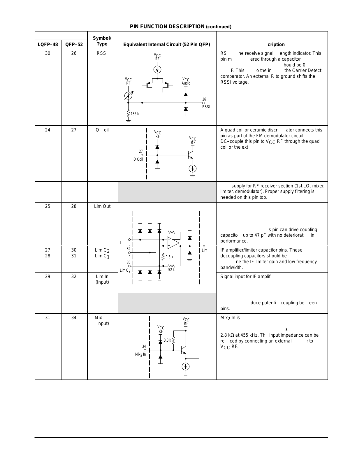
RSSI is the receive signal strength indicator. This
pin must be filtered through a capacitor to ground.
БББББББББББ
The capacitance value range should be 0.01 to
БББББББББББ
0.1 µF. This is also the input to the Carrier Detect
comparator. An external R to ground shifts the
БББББББББББ
RSSI voltage.
БББББББББББ
БББББББББББ
БББББББББББ
БББББББББББ
БББББББББББ
A quad coil or ceramic discriminator connects this
БББББББББББ
pin as part of the FM demodulator circuit.
БББББББББББ
DC–couple this pin to VCC RF through the quad
coil or the external resistor.
БББББББББББ
БББББББББББ
БББББББББББ
БББББББББББ
VCC supply for RF receiver section (1st LO, mixer,
limiter, demodulator). Proper supply filtering is
БББББББББББ
needed on this pin too.
A quad coil or ceramic discriminator are connected
to these pins as part of the FM demodulator circuit.
БББББББББББ
A coupling capacitor connects this pin to the quad
БББББББББББ
coil or ceramic discriminator as part of the FM
demodulator circuit. This pin can drive coupling
БББББББББББ
capacitors up to 47 pF with no deterioration in
БББББББББББ
performance.
IF amplifier/limiter capacitor pins. These
decoupling capacitors should be 0.1 µF. They
БББББББББББ
determine the IF limiter gain and low frequency
БББББББББББ
bandwidth.
Signal input for IF amplifier/limiter. Signals should
be ac–coupled to this pin. The input impedance is
БББББББББББ
1.5 kΩ at 455 kHz.
This pin is not connected internally but should be
БББББББББББ
grounded to reduce potential coupling between
pins.
БББББББББББ
Mix2 In is the second mixer input. Signals are to be
БББББББББББ
ac–coupled to this pin, which is biased internally to
VCC RF. The input impedance is
БББББББББББ
2.8 kΩ at 455 kHz. The input impedance can be
БББББББББББ
reduced by connecting an external resistor to
VCC RF.
БББББББББББ
БББББББББББ
БББББББББББ
БББББББББББ
14
MOTOROLA ANALOG IC DEVICE DATA
LQFP–48
Á
Á
Á
Á
Á
Á
Á
Á
Á
Á
Á
Á
Á
Á
Á
Á
Á
Á
Á
Á
Á
Á
Á
Á
Á
Á
Á
Á
Á
Á
Á
Á
Á
Á
Á
Á
Á
Á
Á
Á
Á
Á
Á
Á
Á
Á
Á
Á
Á
Á
Á
Á
Á
Á
Á
Á
Á
Á
Á
Á
Á
Á
Á
Á
Á
Á
Á
Á
Á
Á
Á
Á
Á
Á
Á
Á
Á
950 950
Á
Á
Á
Á
Á
Á
Á
Á
Á
Á
Á
Á
Á
Á
Á
Á
Á
Á
Á
Á
Á
Á
Á
Á
Á
Á
Á
Á
Á
Á
Á
Á
Á
Á
Á
Á
Á
Á
Á
Á
Á
Á
Á
Á
Á
Á
Á
Á
Á
Á
Á
Á
Á
Á
Á
Á
Á
Á
Á
Á
Á
Á
Á
Á
Á
Á
Á
Á
Á
Á
Á
Á
Á
32
ÁÁ
ÁÁ
ÁÁ
ÁÁ
ÁÁ
Pin
QFP–52
ÁÁ
ÁÁ
ÁÁ
ÁÁ
ÁÁ
35
Symbol/
Symbol/
Type
Type
Mix2 Out
(Output)
ÁÁÁ
ÁÁÁ
ÁÁÁ
ÁÁÁ
ÁÁÁ
MC13110A/B MC13111A/B
PIN FUNCTION DESCRIPTION (continued)
Equivalent Internal Circuit (52 Pin QFP)
Equivalent Internal Circuit (52 Pin QFP)
VCC
RF
ББББББББББ
ББББББББББ
ББББББББББ
ББББББББББ
ББББББББББ
1.2 k
V
CC
RF
35
Mix2 Out
Description
Description
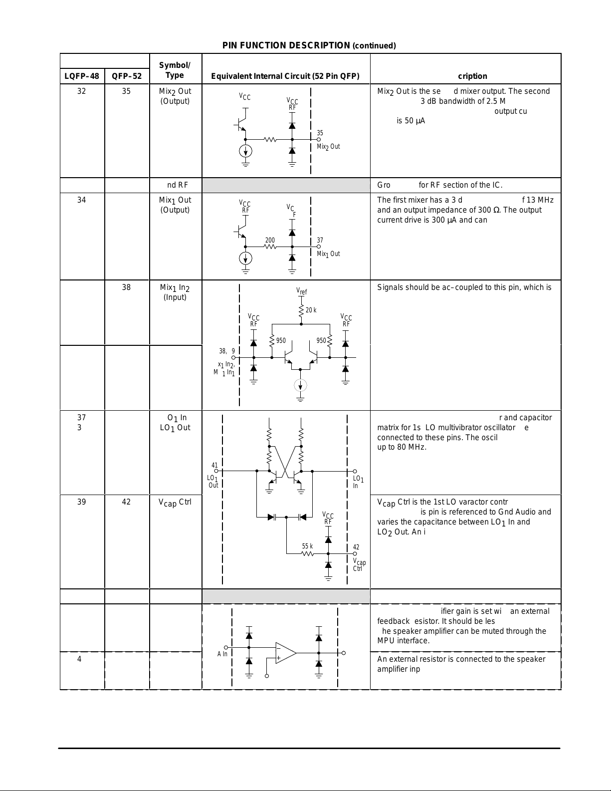
Mix2 Out is the second mixer output. The second
mixer has a 3 dB bandwidth of 2.5 MHz and an
БББББББББББ
output impedance of 1.5 kΩ. The output current
БББББББББББ
drive is 50 µA.
БББББББББББ
БББББББББББ
БББББББББББ
33
34
ÁÁ
ÁÁ
ÁÁ
ÁÁ
ÁÁ
35
ÁÁ
ÁÁ
ÁÁ
36
ÁÁ
ÁÁ
ÁÁ
37
ÁÁ
38
ÁÁ
ÁÁ
ÁÁ
ÁÁ
39
ÁÁ
ÁÁ
ÁÁ
ÁÁ
ÁÁ
40
41
ÁÁ
ÁÁ
42
ÁÁ
ÁÁ
36
37
ÁÁ
ÁÁ
ÁÁ
ÁÁ
ÁÁ
38
ÁÁ
ÁÁ
ÁÁ
39
ÁÁ
ÁÁ
ÁÁ
40
ÁÁ
41
ÁÁ
ÁÁ
ÁÁ
ÁÁ
42
ÁÁ
ÁÁ
ÁÁ
ÁÁ
ÁÁ
43
44
ÁÁ
ÁÁ
45
ÁÁ
ÁÁ
Gnd RF
Mix1 Out
(Output)
ÁÁÁ
ÁÁÁ
ÁÁÁ
ÁÁÁ
ÁÁÁ
Mix1 In
2
(Input)
ÁÁÁ
ÁÁÁ
ÁÁÁ
Mix1 In
1
(Input)
ÁÁÁ
ÁÁÁ
ÁÁÁ
LO1 In
ÁÁÁ
LO1 Out
ÁÁÁ
ÁÁÁ
ÁÁÁ
ÁÁÁ
V
Ctrl
cap
ÁÁÁ
ÁÁÁ
ÁÁÁ
ÁÁÁ
ÁÁÁ
Gnd Audio
SA Out
(Output)
ÁÁÁ
ÁÁÁ
SA In
(Input)
ÁÁÁ
ÁÁÁ
VCC
RF
ББББББББББ
ББББББББББ
ББББББББББ
ББББББББББ
ББББББББББ
ББББББББББ
V
ББББББББББ
ББББББББББ
CC
RF
V
CC
RF
200
V
950 950
ref
20 k
37
Mix1 Out
V
CC
RF
38, 39
Mix1 In2,
ББББББББББ
Mix1 In
1
ББББББББББ
ББББББББББ
ББББББББББ
ББББББББББ
ББББББББББ
41
ББББББББББ
LO
1
Out
ББББББББББ
V
55 k
V
CC
Audio
RF
CC
44
SA Out
ББББББББББ
ББББББББББ
ББББББББББ
ББББББББББ
ББББББББББ
V
CC
Audio
ББББББББББ
45
ББББББББББ
SA In
ББББББББББ
V
ББББББББББ
B
Ground pin for RF section of the IC.
The first mixer has a 3 dB IF bandwidth of 13 MHz
and an output impedance of 300 Ω. The output
БББББББББББ
current drive is 300 µA and can be programmed
БББББББББББ
for 1.0 mA.
БББББББББББ
БББББББББББ
БББББББББББ
Signals should be ac–coupled to this pin, which is
biased internally to VCC – 1.6 V. The single–ended
БББББББББББ
and differential input impedance are about 1.6 and
1.8 kΩ at 46 MHz, respectively.
БББББББББББ
БББББББББББ
БББББББББББ
БББББББББББ
БББББББББББ
Tank Elements, an internal varactor and capacitor
БББББББББББ
matrix for 1st LO multivibrator oscillator are
connected to these pins. The oscillator is useable
БББББББББББ
up to 80 MHz.
БББББББББББ
40
БББББББББББ
LO1
In
БББББББББББ
V
Ctrl is the 1st LO varactor control pin. The
cap
voltage at this pin is referenced to Gnd Audio and
БББББББББББ
varies the capacitance between LO1 In and
LO2 Out. An increase in voltage will decrease
БББББББББББ
capacitance.
42
БББББББББББ
V
cap
БББББББББББ
Ctrl
БББББББББББ
Ground for audio section of the IC.
The speaker amplifier gain is set with an external
feedback resistor. It should be less than 200 kΩ.
БББББББББББ
The speaker amplifier can be muted through the
БББББББББББ
MPU interface.
An external resistor is connected to the speaker
amplifier input (SA In). This will set the gain and
БББББББББББ
input impedance and must be ac–coupled.
БББББББББББ
MOTOROLA ANALOG IC DEVICE DATA
15
LQFP–48
Á
Á
Á
Á
Á
Á
Á
Á
Á
Á
Á
Á
Á
Á
Á
Á
Á
Á
Á
Á
Á
Á
Á
Á
Á
Á
Á
Á
Á
Á
Á
Á
Á
Á
Á
Á
Á
Á
Á
Á
Á
Á
Á
Á
Á
Á
Á
Á
Á
Á
Á
Á
Á
Á
Á
Á
Á
Á
Á
Á
Á
Á
Á
Á
Á
Á
Á
Á
Á
Á
Á
Á
Á
Á
Á
Á
Á
Á
Á
Á
Á
Á
Á
Á
Á
Á
Á
Á
Á
Á
Á
Á
Á
Á
Á
Á
Á
Á
Á
Á
Á
Á
Á
Á
Á
Á
Á
Á
Á
Á
Á
Á
Á
Á
Á
Á
Á
Á
Á
Á
Á
Á
Á
Á
Á
Á
Á
Á
Á
Á
Á
Á
Á
Á
Á
Á
Á
Á
Á
Á
Á
Á
Á
Á
Á
Á
43
ÁÁ
ÁÁ
ÁÁ
ÁÁ
ÁÁ
44
ÁÁ
ÁÁ
ÁÁ
ÁÁ
ÁÁ
ÁÁ
45
ÁÁ
ÁÁ
ÁÁ
ÁÁ
ÁÁ
46
ÁÁ
ÁÁ
ÁÁ
ÁÁ
–
ÁÁ
ÁÁ
–
ÁÁ
ÁÁ
ÁÁ
47
ÁÁ
ÁÁ
ÁÁ
ÁÁ
Pin
QFP–52
ÁÁ
ÁÁ
ÁÁ
ÁÁ
ÁÁ
ÁÁ
ÁÁ
ÁÁ
ÁÁ
ÁÁ
ÁÁ
ÁÁ
ÁÁ
ÁÁ
ÁÁ
ÁÁ
ÁÁ
ÁÁ
ÁÁ
ÁÁ
ÁÁ
ÁÁ
ÁÁ
ÁÁ
ÁÁ
ÁÁ
ÁÁ
ÁÁ
ÁÁ
46
47
48
49
50
51
52
Symbol/
Symbol/
Type
Type
E Out
(Output)
ÁÁÁ
ÁÁÁ
ÁÁÁ
ÁÁÁ
ÁÁÁ
E Cap
ÁÁÁ
ÁÁÁ
ÁÁÁ
ÁÁÁ
ÁÁÁ
ÁÁÁ
E In
(Input)
ÁÁÁ
ÁÁÁ
ÁÁÁ
ÁÁÁ
ÁÁÁ
Scr Out
(Output)
ÁÁÁ
ÁÁÁ
ÁÁÁ
ÁÁÁ
Ref
2
ÁÁÁ
ÁÁÁ
Ref
1
ÁÁÁ
ÁÁÁ
ÁÁÁ
V
B
ÁÁÁ
ÁÁÁ
ÁÁÁ
ÁÁÁ
MC13110A/B MC13111A/B
PIN FUNCTION DESCRIPTION (continued)
Equivalent Internal Circuit (52 Pin QFP)
Equivalent Internal Circuit (52 Pin QFP)
V
CC
V
CC
V
CC
Audio
V
Audio
240
Audio
CC
30 k
V
CC
Audio
V
V
CC
Audio
47
E Cap
B
46
E Out
49
Scr Out
52
V
B
ББББББББББ
ББББББББББ
ББББББББББ
ББББББББББ
V
B
ББББББББББ
V
40 k
CC
Audio
ББББББББББ
ББББББББББ
ББББББББББ
ББББББББББ
ББББББББББ
ББББББББББ
Audio
ББББББББББ
ББББББББББ
48
E In
ББББББББББ
ББББББББББ
ББББББББББ
ББББББББББ
ББББББББББ
ББББББББББ
ББББББББББ
V
B
ББББББББББ
ББББББББББ
50, 51
Ref2, Ref
1
ББББББББББ
ББББББББББ
ББББББББББ
VCC
Audio
ББББББББББ
ББББББББББ
ББББББББББ
ББББББББББ
Description
Description
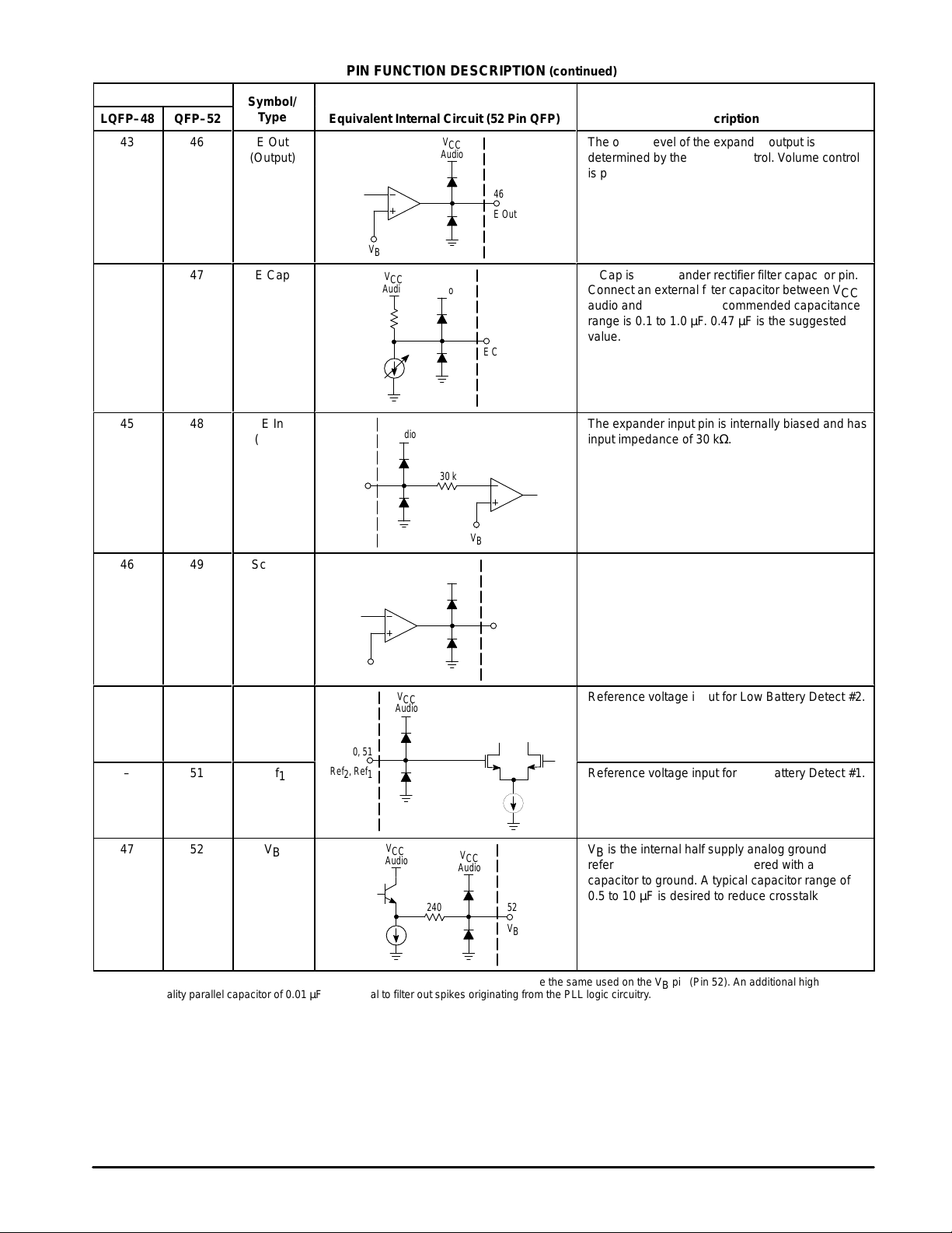
The output level of the expander output is
determined by the volume control. Volume control
БББББББББББ
is programmable through the MPU interface.
БББББББББББ
БББББББББББ
БББББББББББ
БББББББББББ
E Cap is the expander rectifier filter capacitor pin.
БББББББББББ
Connect an external filter capacitor between V
БББББББББББ
audio and E Cap. The recommended capacitance
range is 0.1 to 1.0 µF. 0.47 µF is the suggested
БББББББББББ
value.
БББББББББББ
БББББББББББ
БББББББББББ
CC
The expander input pin is internally biased and has
input impedance of 30 kΩ.
БББББББББББ
БББББББББББ
БББББББББББ
БББББББББББ
БББББББББББ
Scr Out is the Rx audio output. An internal low
pass filter has a –3 dB bandwidth of 4.0 kHz.
БББББББББББ
БББББББББББ
БББББББББББ
БББББББББББ
Reference voltage input for Low Battery Detect #2.
БББББББББББ
БББББББББББ
Reference voltage input for Low Battery Detect #1.
БББББББББББ
БББББББББББ
БББББББББББ
VB is the internal half supply analog ground
reference. This pin must be filtered with a
БББББББББББ
capacitor to ground. A typical capacitor range of
0.5 to 10 µF is desired to reduce crosstalk and
БББББББББББ
noise. It is important to keep this capacitor value
equal to the PLL V
БББББББББББ
(Note 9).
БББББББББББ
capacitor due to logic timing
ref
NOTE: 9.A capacitor range of 0.5 to 10 µF is recommended. The capacitor value should be the same used on the VB pin (Pin 52). An additional high
ББББББББББББББББББББББББББББББББ
16
quality parallel capacitor of 0.01 µF is essential to filter out spikes originating from the PLL logic circuitry.
MOTOROLA ANALOG IC DEVICE DATA
MC13110A/B MC13111A/B
ББББББББББББББББ
Á
ББББББББББББББББ
Á
DEVICE DESCRIPTION AND APPLICATION INFORMATION
The following text, graphics, tables and schematics are
provided to the user as a source of valuable technical
information about the Universal Cordless Telephone IC. This
information originates from thorough evaluation of the device
performance for the US and French applications. This data
was obtained by using units from typical wafer lots. It is
important to note that the forgoing data and information was
from a limited number of units. By no means is the user to
assume that the data following is a guaranteed parametric.
Only the minimum and maximum limits identified in the
electrical characteristics tables found earlier in this spec are
guaranteed.
General Circuit Description
The MC131 10A/B and MC13111A/B are a low power dual
conversion narrowband FM receiver designed for
applications up to 80 MHz carrier frequency. This device is
primarily designated to be used for the 49 MHz cordless
phone (CT–0), but has other applications such as low data
rate narrowband data links and as a backend device for 900
MHz systems where baseband analog processing is
required. This device contains a first and second mixer,
limiter, demodulator, extended range receive signal strength
(RSSI), receive and transmit baseband processing, dual
programmable PLL, low battery detect, and serial interface
for microprocessor control. The FM receiver can also be
used with either a quadrature coil or ceramic resonator.
Refer to the Pin Function Description table for the simplified
internal circuit schematic and description of this device.
DC Current and Battery Detect
Figures 3 through 6 are the current consumption for
Inactive, Standby , Receive, and Active modes versus supply
voltages. Figures 7 and 8 show the typical behavior of current
consumption in relation to temperature. The relationship of
additional current draw due to IP3 bit set to <1> and supply
voltage are shown in Figures 9 and 10.
For the Low Battery Detect, the user has the option to
operate the IC in the programmable or non–programmable
modes. Note that the 48 pin package can only be used in the
programmable mode. Figure 128 describes this operation
(refer to the Serial Interface section under Clock Divider
Register).
In the programmable mode several different internal
threshold levels are available (Figure 2). The bits are set
through the SCF Clock Divider Register as shown in Figures
108 and 126. The reference for the internal divider network is
VCC Audio. The voltages on the internal divider network are
compared to the Internal Reference Voltage, VB, generated
by an internal source. Since the internal comparator used is
non–inverting, a high at VCC Audio will yield a high at the
battery detect output, and vice versa for VCC Audio set to a
low level. For the 52 pin package option, the Ref 1 and Ref 2
pins need to be tied to VCC when used in the programmable
mode. It is essential to keep the external reference pins
above Gnd to prevent any possible power–on reset to be
activated.
When considering the non–programmable mode (bits set
to <000>) for the 52 pin package, the Ref 1 and Ref 2 pins
become the comparators reference. An internal switch is
activated when the non–programmable mode is chosen
connecting Ref 1 and Ref 2. Here, two external precision
resistor dividers are used to set independent thresholds for
two battery detect hysteresis comparators. The voltages on
Ref 1 and Ref 2 are again compared to the internally
generated 1.5 V reference voltage (VB).
The Low Battery Detect threshold tolerance can be
improved by adjusting a trim–pot in the external resistor
divider (user designed). The initial tolerance of the internal
reference voltage (VB) is ±6.0%. Alternately , the tolerance of
the internal reference voltage can be improved to ±1.5%
through MPU serial interface programming (refer to the Serial
Interface section, Figure 131). The internal reference can be
measured directly at the “VB” pin. During final test of the
telephone, the VB internal reference voltage is measured.
Then, the internal reference voltage value is adjusted
electronically through the MPU serial interface to achieve the
desired accuracy level. The voltage reference register value
should be stored in ROM during final test so that it can be
reloaded each time the combo IC is powered up. The Low
Battery Detect outputs are open collector. The battery detect
levels will depend on the accuracy of the VB voltage. Figure
12 indicates that the VB voltage is fairly flat over temperature.
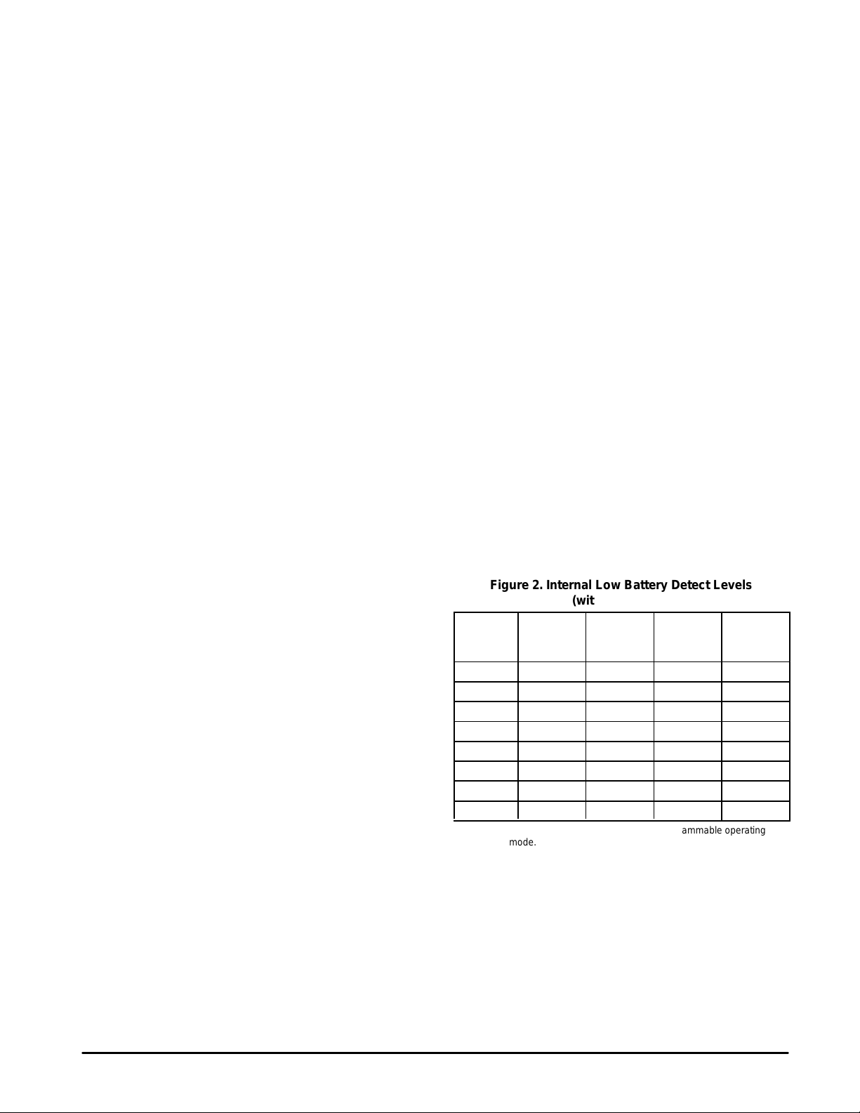
Figure 2. Internal Low Battery Detect Levels
БББББББББББББББ
Battery
Detect
Select
0 – – – –
1 2.867 2.861 2.864 4.0
2 2.953 2.947 2.950 6.0
3 3.039 3.031 3.035 8.0
4 3.207 3.199 3.204 8.0
5 3.291 3.285 3.288 6.0
6 3.375 3.367 3.371 8.0
7 3.461 3.453 3.457 8.0
NOTE: 10. Battery Detect Select 0 is the non–programmable operating
БББББББББББББББ
Ramping
mode.
(with VB = 1.5 V)
Ramping
Up
(V)
Down
(V)
Average
(V)
Hysteresis
(mV)
MOTOROLA ANALOG IC DEVICE DATA
17

MC13110A/B MC13111A/B
Figure 3. Current versus Supply
40
A)
35
µ
30
25
20
15
IC, SUPPLY CURRENT (
10
INACT
5.0
I
0
2.7 3.1 3.5 3.9 4.3 4.7 5.1 5.5
V oltage Inactive Mode
VCC, SUPPLY VOLTAGE (V)
DC CURRENT
, SUPPLY CURRENT (mA)
CC
STD I
Figure 4. Current versus Supply
V oltage Standby Mode, MCU
Clock Output – On at 2.048 MHz
1.0
0.9
0.8
0.7
0.6
0.5
0.4
0.3
0.2
0.1
0
2.7 3.1 3.5 3.9 4.3 4.7 5.1 5.5
VCC, SUPPLY VOLTAGE (V)
MCU Clock Out On
MCU Clock Out Off
Figure 5. Current versus Supply
V oltage Receive Mode
5.0
4.9
4.8
4.7
4.6
4.5
4.4
, SUPPLY CURRENT (mA)
4.3
CC
I
4.2
x
R
4.1
4.0
2.7 3.1 3.5 3.9 4.3 4.7 5.1 5.5
VCC, SUPPLY VOLTAGE (V)
MCU Clock Out On
MCU Clock Out Off
Figure 7. Current versus
T emperature Normalized to 25°C
15
°
10
5.0
0
–5.0
DELTA CURRENT DRAIN (% FROM 25 C)
–10
–40 –30 –20 –10 0 10 20 30 40 50 60 70 80 90
°
TA, TEMPERATURE (
C)
Standby
Inactive
Figure 6. Current versus Supply V oltage
Active Mode
8.0
7.9
7.8
7.7
7.6
7.5
7.4
7.3
CC
7.2
ACT I , SUPPLY CURRENT (mA)
7.1
7.0
2.7 3.1 3.5 3.9 4.3 4.7 5.1 5.5
VCC, SUPPLY VOLTAGE (V)
MCU Clock Out On
MCU Clock Out Off
Figure 8. Current versus
T emperature Normalized to 25°C
6.0
°
4.0
2.0
0
–2.0
–4.0
–6.0
–8.0
–10
DELTA CURRENT DRAIN (% FROM 25 C)
–12
–40 –30 –20 –10 10 20 30 40 50 60 70 80 90
0
TA, TEMPERATURE (
°
C)
Receive
Active
18
MOTOROLA ANALOG IC DEVICE DATA
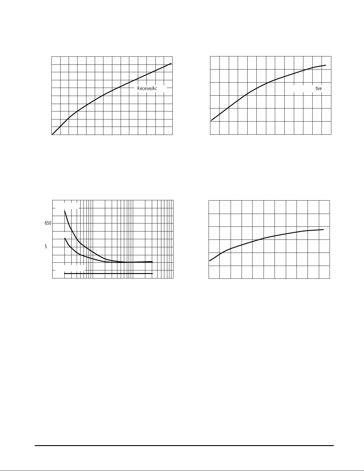
MC13110A/B MC13111A/B
Figure 9. Additional Supply Current Consumption
1.50
1.48
1.46
1.44
1.42
1.40
1.38
1.36
1.34
DELTA CURRENT DRAIN (mA)
1.32
1.30
2.7 2.9 3.1 3.3 3.5 3.7 3.9 4.1 4.3 4.5 4.7 4.9 5.1 5.3 5.5
versus Supply V oltage, IP3 = <1>
Receive/Active
VCC, SUPPLY VOLTAGES (V)
DC CURRENT
°
DELTA CURRENT DRAIN (% FROM 25 C)
Figure 10. Additional IP3
Supply Current Consumption versus
T emperature Normalized to 25°C
10
5
0
Receive/Active
–5
–10
–15
–20
–40 –30 –20 –10 0 10 20 30 40 50 60 70 80 90
TA, TEMPERATURE (
°
C)
Figure 11. Current Standby
800
750
700
650
600
550
500
450
CC
400
STD I , SUPPLY CURRENT (mA)
350
300
1.0 10 100 1000
Mode versus MCU Clock Output
10 pF load
No load
MCU clock off
MCU CLK OUT DIVIDE VALUE
Figure 12. VB V oltage versus Temperature
Normalized to 1.5 V at 25°C
1.5075
1.5050
1.5025
1.5000
1.4975
1.4950
s
V , NORMALIZED VB VOLTAGE (V)
1.4925
–20–100 102030405060708090
°
TA, TEMPERATURE (
C)
MOTOROLA ANALOG IC DEVICE DATA
19
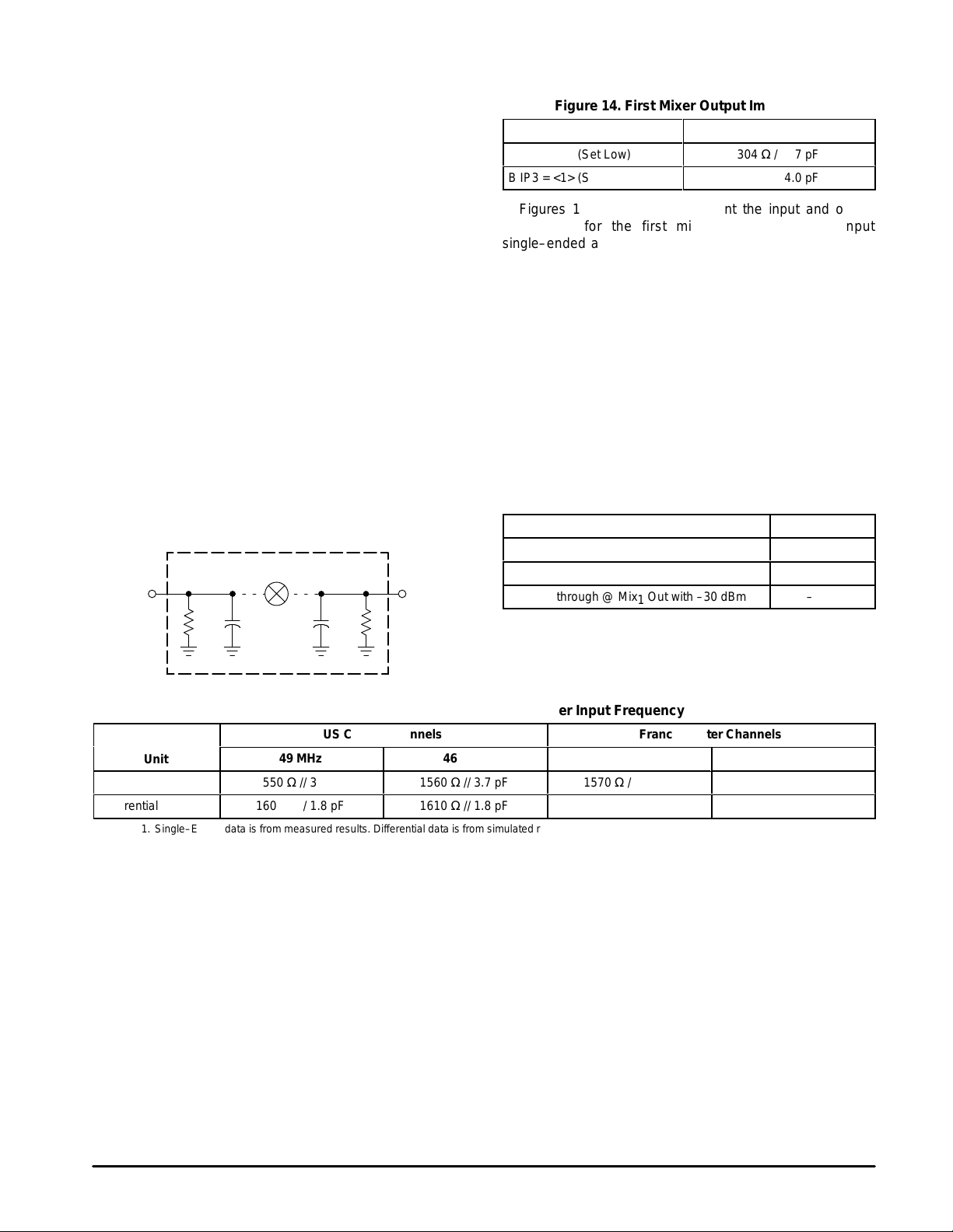
MC13110A/B MC13111A/B
ББББББББББББББББ
ББББББББ
ББББББББ
ББББББББ
ББББББББББББББББ
ББББББББББББ
ББББББББББББ
ББББББББББББ
ББББББББББББ
БББББББ
БББББББ
БББББББ
FIRST AND SECOND MIXER
Mixer Description
The 1st and 2nd mixers are similar in design. Both are
double balanced to suppress the LO and the input
frequencies to give only the sum and difference frequencies
at the mixer output. Typically the LO is suppressed better
than –50 dB for the first mixer and better than –40 dB for the
second mixer. The gain of the 1st mixer has a –3.0 dB corner
at approximately 13 MHz and is used at a 10.7 MHz IF . It has
an output impedance of 300 Ω and matches to a typical
10.7 MHz ceramic filter with a source and load impedance of
330 Ω. A series resistor may be used to raise the impedance
for use with crystal filters. They typically have an input
impedance much greater than 330 Ω.
First Mixer
Figures 17 through 20 show the first mixer transfer curves
for the voltage conversion gain, output level, and
intermodulation. Notice that there is approximately 10 dB
linearity improvement when the “IP3 Increase” bit is set to
<1>. The “IP3 Increase” bit is a programmable bit as shown in
the Serial Programmable Interface section under the R
Counter Latch Register. The IP3 = <1> option will increase
the supply current demand by 1.3 mA.
Figure 13. First Mixer Input and Output Impedance
Schematic
1st Mixer
Mix1 In Mix1 Out
R
C
PI
C
PI
PO
R
PO
БББББББББББББББ
БББББББ
БББББББ
БББББББ
Figure 14. First Mixer Output Impedance
Unit
B IP3 = <0> (Set Low)
B IP3 = <1> (Set High)
БББББББ
БББББББ
БББББББ
Output Impedance
304 Ω // 3.7 pF
300 Ω // 4.0 pF
Figures 13, 14, and 16 represent the input and output
impedance for the first mixer. Notice that the input
single–ended and differential impedances are basically the
same. The output impedance as described in Figure 14 will
be used to match to a ceramic or crystal filter’s input
impedance. A typical ceramic filter input impedance is 330 Ω
while crystal filter input impedance is usually 1500 Ω. Exact
impedance matching to ceramic filters are not critical,
however, more attention needs to be given to the filter
characteristics of a crystal filter. Crystal filters are much
narrower. It is important to accurately match to these filters to
guaranty a reasonable response.
T o find the IF bandwidth response of the first mixer refer to
Figure 22. The –3.0 dB bandwidth point is approximately 13
x
MHz. Figure 15 is a summary of the first mixer feedthrough
parameters.
Figure 15. First Mixer Feedthrough Parameters
Parameter
1st LO Feedthrough @ Mix1 In
1st LO Feedthrough @ Mix1 Out
RF Feedthrough @ Mix1 Out with –30 dBm
1
(dBm)
–70.0
–55.5
–61.0
Figure 16. First Mixer Input Impedance over Input Frequency
US Center Channels
Unit
Single–Ended
Differential
Note: 1 1. Single–Ended data is from measured results. Differential data is from simulated results.
49 MHz
1550 Ω // 3.7 pF
1600 Ω // 1.8 pF
46 MHz
1560 Ω // 3.7 pF
1610 Ω // 1.8 pF
France Center Channels
41 MHz
1570 Ω // 3.8 pF
1670 Ω // 1.8 pF
26 MHz
1650 Ω // 3.7 pF
1710 Ω // 1.8 pF
20
MOTOROLA ANALOG IC DEVICE DATA
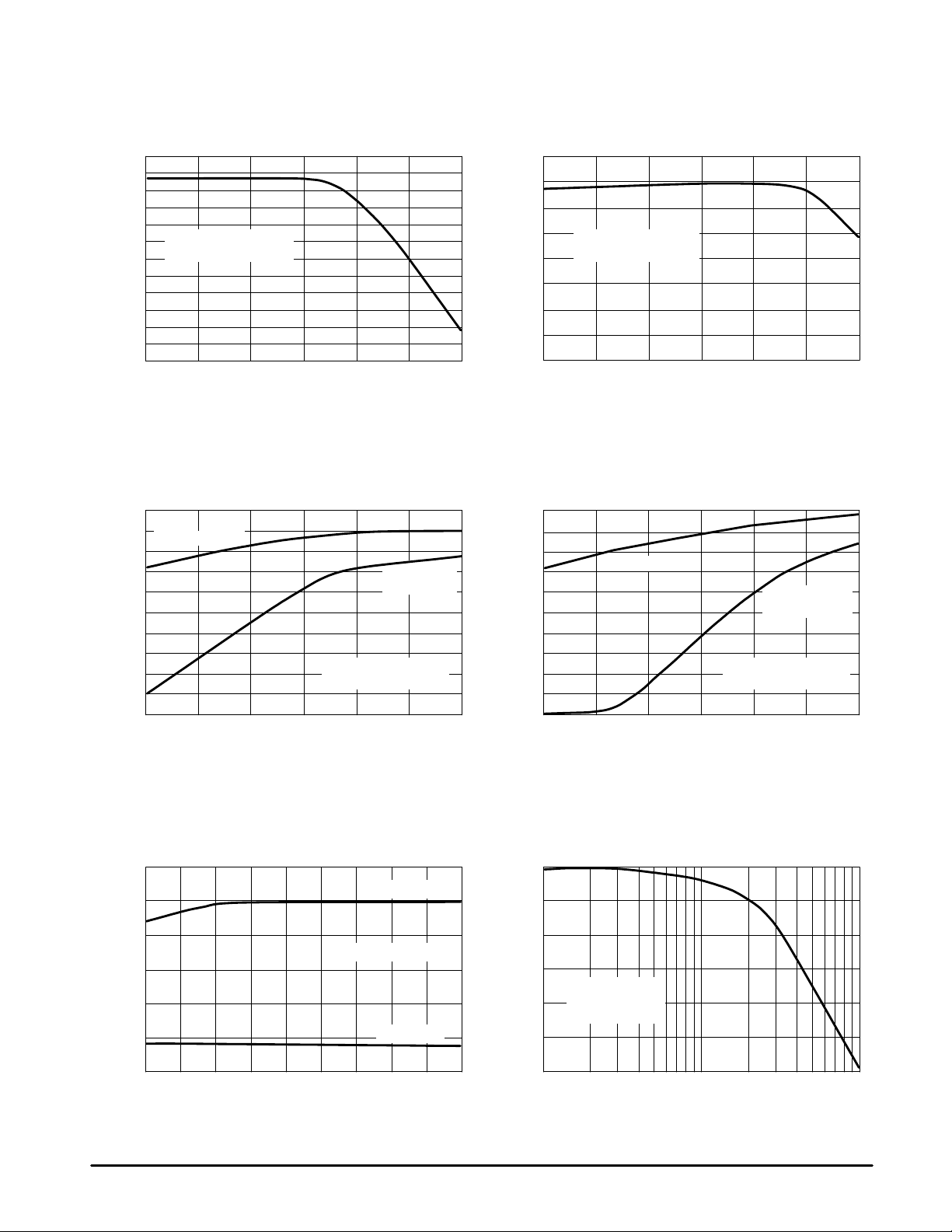
MC13110A/B MC13111A/B
FIRST MIXER
Figure 17. First Mixer V oltage Conversion
14
12
10
VCC = 3.6 V
, VOLTAGE
gain1
MX
CONVERSION GAIN (dB)
IF = 10.695 MHz, 330
8.0
6.0
4.0
2.0
–40
Figure 19. First Mixer Output Level and
0
Fundamental Level
–20
–40
Out, MIXER OUTPUT (dBm)
1
Mix
Gain, IP3_bit = 0
Ω
Mix1 In, MIXER INPUT LEVEL (dBm)
Intermodulation, IP3_bit = 0
3rd Order
Intermodulation
VCC = 3.6 V
IF = 10.695 MHz, 330
Figure 18. First Mixer V oltage Conversion
Gain, IP3_bit = 1
14
12
VCC = 3.6 V
10
, VOLTAGE
gain1
MX
8.0
CONVERSION GAIN (dB)
6.0
–40
IF = 10.695 MHz, 330
–35–35 –30–30 –25–25 –20–20 –15–15 –10–10
Mix1 In, MIXER INPUT LEVEL (dBm)
Ω
Figure 20. First Mixer Output Level and
Intermodulation, IP3_bit = 1
0
–20
–40
–60–60
Out, MIXER OUTPUT (dBm)
1
Ω
Mix
–80–80
Fundamental Level
3rd Order
Intermodulation
VCC = 3.6 V
IF = 10.695 MHz, 330
Ω
–40
–35 –30–30 –25–25 –20
Mix1 In, MIXER INPUT LEVEL (dBm)
Figure 21. First Mixer Compression versus
–10
–12
–14
, 1.0 dB
1
–16
1.0 dB Mix
–18
O
V
–20
VOLTAGE COMPRESSION (dBm)
2.7
3.3
VCC Audio, AUDIO SUPPLY VOLTAGE (V)
–20 –15
Supply V oltage
IF = 10.695 MHz, 330
4.2
–15 –10
–10
–100–100
–40
–35
Mix1 In, MIXER INPUT LEVEL (dBm)
Figure 22. First IF Bandwidth
15
IP3_bit = 1
IP3_bit = 0
4.8
Ω
5.4
10
5.0
0
, VOLTAGE
gain1
–5.0
MX
CONVERSION GAIN (dB)
–10
–15–22
VCC = 3.6 V
RL = 330
LO = 36.075 MHz
1.0
Ω
10
f, IF FREQUENCY (MHz)
1003.6 3.9 4.53.0 5.1
MOTOROLA ANALOG IC DEVICE DATA
21
 Loading...