

Motorola MC13081XB Datasheet
Order this document by MC13081X/D
The MC13081X includes all the signal processing functions for a scan
frequency agile and multiple sync system analog RGB monitor and includes
the following functions:
• Automatic Horizontal Frequency Tracking of All Commonly Used
Personal Computers, Continuously Adaptable from 30 kHz to 64 kHz
• Sync–on–Green Detection
• Vertical Timebase Operates from 45 to 100 Hz
• Vertical and Horizontal Sync Polarity Detection with Outputs for
Mode Switching
• Video Pre–Amplifiers T ypical Rise/Fall Time of 5.0 ns at 3.0 Vpp Output
Voltage Swing
• Overall Contrast Control and Independent RGB Gain Controls
MULTIMODE COLOR
MONITOR PROCESSOR
SEMICONDUCTOR
TECHNICAL DATA
56
1
B SUFFIX
PLASTIC SDIP PACKAGE
CASE 859
ORDERING INFORMATION
Operating
Device
MC13081XB
Temperature Range
TA = 0° to +70°C Plastic SDIP
Package
CC2
Timebase V
Horizontal Position
56
55
2
1
Vertical Osc Cap
Vertical Sync Det
Horizontal Sync Det
54
53
4
3
Vertical Hold
Vertical TTL Sync
Vertical Intergrator Cap
Vertical Size
N/C
Vertical Ramp Cap
50
51
52
5
6
7
N/C
Composite Video In
Horizontal TTL Sync
N/C
Vertical Ramp Out
Video Blanking In
47
48
49
8
9
10
N/C
PD1
5.0 V Reg
PIN CONNECTIONS
Horizontal Drive Width
Horizontal Drive
Horizontal Flyback
PD2
45
46
11
12
AFC
Horizontal Freq Control
Horizontal Drive Gnd
42
43
44
13
141516
FHIA
FH Switch A
Timebase Gnd
(Top View)
Channel 1 Emitter Out
Channel 1 Collector Out
X–Ray Shutdown
40
41
17
FHIB
FH Switch B
Channel 2 Collector Out
Channel 1 Clamp
37
38
39
18
20
19
Contrast
Brightness
Channel 1 Subcontrast
N/C
N/C
Channel 2 Emitter Out
34
36
35
21
23
22
N/C
N/C
Channel 1 Video In
CC1
Channel 3 Emitter Out
Channel 2 Clamp
Channel 3 Collector Out
32
33
24
25
Channel 2 Video In
Channel 2 Subcontrast
Video V
Channel 3 Clamp
31
29
30
26
27
28
Video Gnd
Channel 3 Video In
Channel 3 Subcontrast
This document contains information on a new product. Specifications and information herein
are subject to change without notice.
MOTOROLA ANALOG IC DEVICE DATA
Motorola, Inc. 1996 Rev 0
1
Vert Integrator Cap
PD1F
AFC
Hori Freq Control
Timebase V
CC
MC13081X
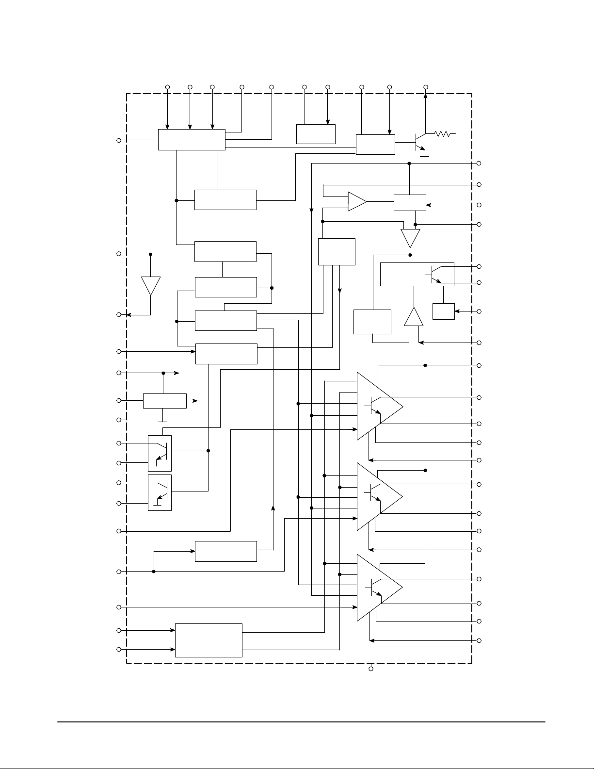
Figure 1. Block Diagram
TTL
TTL
H–Sync
V–Sync
4 5 6 53 54 1 51 52 48
3
10
11
12
56
Sync Source Decoder
and Polarity Control
H–Sync V–Sync
64 H
X1
Clamp Pulse Decoder
V–Sync
CVS
Polar Det
5 Count Latch
Phase Detector
UpDown
Digital Horizontal
Lock Control
64 Divider and
64x Oscillator
H–Sync
Polar Det
V
osc
Oscillator
Blanking
Vert Hold
Vertical
2
#1 Ramp
Generator
1/8 Line
Shift
Vert
Ramp Cap
Vertical Ramp
Generator
1
Ramp 1
#2 Ramp
Generator
Vert
Size
Horizontal
Ramp 2
Phase
Detector
Driver
2
3
Vert
Ramp
10 K
X–Ray
Ω
V
CC
47
Blanking
55
Hori Position Adjust
46
H–Flyback
45
PD2F
43
H–Drive
42
Timebase Gnd
41
X–Ray Shutdown
44
H–Drive Width Adjust
29
Video V
CC
+5.0 V Output
Timebase Gnd
FHA Switch
FHA Threshold
FHB Switch
FHB Threshold
Channel 1 Video In
Channel 2 Video In
Channel 3 Video In
Contrast
Brightness
9
13
14
15
16
17
23
25
27
18
19
5 V Regulator
Pulse Position
SOG Detector
Brightness and
Contrast Processor
Clamp
Channel 1
Channel 2
Channel 3
40
Collector Out
39
Emitter Out
38
Clamp
20
Subcontrast
37
Collector Out
34
Emitter Out
33
Clamp
24
Subcontrast
32
Collector Out
31
Emitter Out
30
Clamp
26
Subcontrast
28
Video Gnd
This device contains 1074 active transistors.
2
MOTOROLA ANALOG IC DEVICE DATA
MC13081X
MAXIMUM RATINGS (T
Rating Pin Value Unit
Power Supply Voltage Vdc
Video Section V
Timebase Section V
Brightness, Contrast, Horizontal Flyback
Input, Frequency Switch when Off
X–Ray Shutdown 41 –0.5, +0.9 Vdc
Subcontrast RGB Controls 20, 24, 26 0 to +2.0 Vdc
Horizontal Drive Width, Horizontal Position 44, 55 0 to +5.0 Vdc
Voltage on Horizontal Drive when Off, Vertical
TTL Sync Input, Horizontal TTL Sync Input,
Composite Video Sync Input, Video Amplifier
Output Collectors
Current into Horizontal Drive when On 43 100 mA
Current into Frequency Switch when On 14, 16 30 mA
Video Amplifier Inputs 23, 25, 27 –0.5, + 5.0 Vdc
Video Amplifier Output Current (Total for the
Three Channels)
Storage Temperature – –65 to +150 °C
Junction Temperature – +150 °C
NOTE: ESD data available upon request.
CC1
= 25°C, unless otherwise noted.)
A
CC2
29 –0.5, +10
56 –0.5, +10
19, 18, 46,
14, 16
43, 4, 5, 6,
32, 37, 40
40, 39, 37,
34, 32, 31
0 to V
CC
–0.5 to
VCC + 0.5
120 mA
Vdc
Vdc
RECOMMENDED OPERATING CONDITIONS
Characteristic
Power Supply Voltage Vdc
Video Section V
Timebase Section V
Power Supply Voltage Dif ference, V
Internal 5.0 V Regulator Output Current 9 –20 – 0 mA
Contrast Control 18 0 – 5.0 Vdc
Brightness Control 19 0 – 5.0 Vdc
Subcontrast Control 20, 24, 26 0 – 2.0 Vdc
Horizontal Drive Width Adjust 44 0 – 5.0 Vdc
Horizontal Position Adjust 55 1.0 – 4.0 Vdc
Horizontal Flyback Signal Amplitude 46 0.7 5.0 8.0 V
Horizontal Flyback Signal DC Input Voltage Level 46 –0.2 0 – Vdc
Voltage on Horizontal Drive Collector when “Off” 43 0 – V
Current into Horizontal Drive Collector when “On” 43 0 – 40 mA
Voltage on Horizontal Drive Emitter W.R.T. Circuit Ground 42 –0.3 0 2.0 Vdc
Blanking Input Signal Amplitude 47 1.5 – 4.0 V
Voltage on FH Switches when “Off” 14, 16 0 – 8.0 Vdc
Current into each FH Switch when “On” 14, 16 0 – 20 mA
X–Ray Shutdown 41 0 – 0.7 Vdc
Composite Video Sync Input 6 1.0 – 2.0 Vpp
Vertical Sync Frequency – 45 – 100 Hz
Horizontal Sync Frequency – 30 – 64 kHz
Vertical Sync Pulse Width – – 70 – µs
Horizontal Sync Pulse Width – – 1.0 – µs
CC1
CC2
CC2
– V
CC1
Pin Min Typ Max Unit
29 7.6 8.0 8.4
56 7.6 8.0 8.4
– –0.3 0 0.8 Vdc
CC
V
MOTOROLA ANALOG IC DEVICE DATA
3
MC13081X
(B)
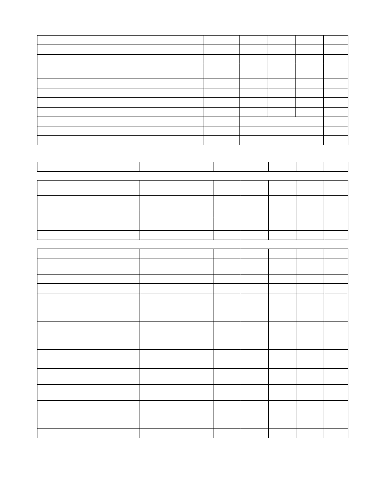
RECOMMENDED OPERATING CONDITIONS
Characteristic UnitMaxTypMinPin
Video Signal Amplitude (with 75 ΩTermination) 23, 25, 27 0.5 0.7 1.2 Vpp
Voltage on Video Amplifier Collector 32, 37, 40 4.5 – V
Current Through Video Collector–Emitter 40, 39, 37 0 – 40 mA
Vertical Hold Set Resistance, R9 + VR2 (Figure 2) 2 – 10 – kΩ
Vertical Size Set Resistance, R10 + VR3 (Figure 2) 52 – 220 – kΩ
Vertical Linearity Set Resistance, R12 + VR4 (Figure 2) 51 – 1000 – kΩ
Operating Ambient Temperature – 0 25 70 °C
FH Switches Set Resistance 15, 17 See Application Section 5 –
Vertical TTL Sync Input 4 TTL Voltage Level Vdc
Horizontal TTL Sync Input 5 TTL Voltage Level Vdc
ELECTRICAL CHARACTERISTICS (T
Characteristic
POWER SUPPLIES
Supply Current – 29, 56 70 85 110 mA
T otal Consumption
5.0 V Regulator 9
Output Voltage Load Current (IB) = 0 mA
Line Regulation
Load Regulation
T emperature Coef ficient – –0.3 – mV/°C
Thermal Resistance, Junction–to–Ambient – – – 59 – °C/W
HORIZONTAL PROCESSING
Horizontal Oscillator Frequency Range – 43 30 – 64 kHz
Horizontal Oscillator Free Running
Frequency @ I12 = 240 µA
Horizontal Sync Detector Output/+VE Sync – 54 – 0 – Vdc
Horizontal Sync Detector Output/–VE Sync – 54 – 3.6 – Vdc
Horizontal Sync Input – 5
Input Impedance – 22 0 kΩ
Input Level – Low 0 – 0.8 Vdc
Input Level – High 2.4 – 5.0 Vdc
Composite Video Sync Input – 6
Input Impedance – 1.0 – kΩ
Internal Bias Level – 1.55 – Vdc
Minimum Input Amplitude 0.1 – – Vpp
Short Term Horizontal Pull–In Range Time < 5.0 ms – – ±5.0 – %FH
Long Term Horizontal Pull–In Range Time > 500 ms – 30 – 64 kHz
Horizontal Frequency Control (Current
Transfer Constant)
Horizontal Free Running Frequency
Change versus Temperature
FH Switch Threshold Pins – 15, 17
Output Current – I12/2 – µA
Threshold – 5.0 – V
Hysteresis 0 – 200 mV
FH Switch Voltage when “On” I = 10 mA 14, 16 – – 200 mVdc
(continued)
CC
34, 32, 31
= 25°C, VCC = 8.0 Vdc)
A
Condition Pin Min Typ Max Unit
7.6 V < VCC < 8.4 V, IB = 0 mA
–10 mA < IB < 0 mA
Sink 240 µA from Pin 12 with
Resistor R5 Opened
Current Flowing Out of Pin 12 12 115 122 129 Hz/µA
Pin 11 is Opened – – 300 – ppm/°C
43 29 31 33 kHz
4.75 5.0 5.25 Vdc
– 25 – mV
– 100 – mV
Vdc
4
MOTOROLA ANALOG IC DEVICE DATA
MC13081X
ELECTRICAL CHARACTERISTICS (continued) (T
Characteristic UnitMaxTypMinPinCondition
HORIZONTAL DRIVE
Horizontal Position Adjust 0 < V55 < 5.0 V, 55
Range FH = 30 k – 56 kHz – 10 – %
Input Impedance See Application Section 7 – 31 – kΩ
Horizontal Drive Width Adjust FH = 35 kHz, 0 < V44 < 5.0 V 44
Range 2:1 – 1:2 %
Input Impedance – 30 – kΩ
Horizontal Flyback See Application Section 4 46
Threshold Input Signal Should Not Fall – 0.7 – V
Input Amplitude Below –0.2 V 0 – 8.0 V
Input Impedance – 10 – kΩ
Horizontal Drive 43
Output Low I
Output High V43 = V
Time Delay from Flyback to Video Output
Blanking
Time Delay from Blanking to Video Output
Blanking
X–Ray Shutdown See Application Section 11 41 0.4 0.58 0.7 Vdc
Activate Voltage
Temperature Coefficient of X–Ray
Threshold Voltage
Horizontal Jitter 30 kHz < FH < 56 kHz 43 – 3.0 – ns
VERTICAL PROCESSING
Vertical Ramp Frequency – 48 45 – 100 Hz
Vertical Ramp FV = 50 Hz, 48
Amplitude R12 + VR4 = 820 kΩ – 3.0 – Vpp
Minimum Peak R10 + VR3 =120 kΩ, – 1.9 – V
Maximum Peak C6 = C7 = 1.0 µ F – 3.4 – V
Output Current – 2.0 – mA
Non–Linearity – 0.45 1.0 %
Vertical Ramp Free Running Temperature
Drift
Vertical Ramp Free Running Drift with V
Vertical Ramp Discharge Rate (Retrace) FV = 50 Hz 48 – 9.5 – V/ms
Vertical Sync Detector Output/+VE Sync 53 – 0 – Vdc
Vertical Sync Detector Output/–VE Sync 53 – 3.6 – Vdc
Vertical Sync Input – 4
Input Impedance – 22 – kΩ
Input Level – Low 0 – 0.8 Vdc
Input Level – High 2.4 – 5.0 Vdc
VIDEO AMPLIFIERS
Input Impedance – 23, 25,27 100 – – kΩ
Internal DC Bias Voltage – 2.4 – Vdc
Output Signal Amplitude Vin = 0.7 Vpp, V18 = 5.0 V 39, 34, 31 – 3.6 – Vpp
Voltage Gain V20 = V24 = V26 = 0 V – 5.1 – V/V
Contrast Control V18 = 0 to 5.0 V;
Subcontrast Control V20, 24, 26 = 2.0 to 0 V;
Brightness Control V19 = 0 to 5.0 V, Measure
CC
See Application Section 7 – – 250 – ns
See Application Section 7 – – 400 – ns
Pin 39, 34, 31 DC Level
= 25°C, VCC = 8.0 Vdc)
A
= 40 mA 0 – 0.3 Vdc
sink
CC
– 41 – –2.3 – mV/°C
FV = 50 Hz 48 – 0.01 – Hz/°C
FV = 50 Hz 48 – 0.5 – Hz/V
18 – 20 – dB
V20, 24, 26 = 0 V
20, 24, 26 1:2.5 – – –
V18 = 5.0 V
19 – ±0.5 – Vdc
– – 100 µA
MOTOROLA ANALOG IC DEVICE DATA
5
MC13081X
p
in
pp;
out
pp
,,
I2
ELECTRICAL CHARACTERISTICS (continued)
(TA = 25°C, VCC = 8.0 Vdc)
Characteristic UnitMaxTypMinPinCondition
VIDEO AMPLIFIERS
Emitter DC Level 39, 34, 31 Vdc
Minimum Brightness V19 = 0 V – 1.0 –
Nominal Brightness V19 = 2.5 V 1.25 1.5 1.75
Maximum Brightness V19 = 5.0 V – 2.0 –
Crosstalk, Amplifier to Amplifier Frequency = 10 MHz 39, 34, 31 – 34 – dB
Output Rise Time Vin = 0.7 Vpp; V
Output Fall Time
= 3.0 Vpp 39, 34, 31 – 5.0 – ns
out
– 5.0 –
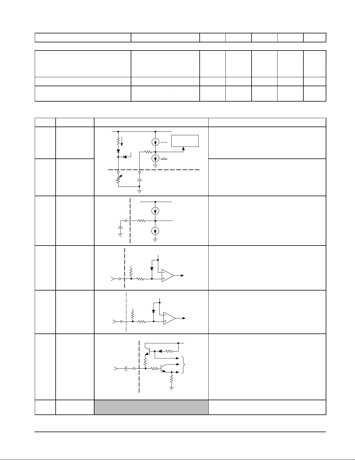
PIN FUNCTION DESCRIPTION
Pin Name Equivalent Internal Circuit Description
I2
10.7
I2
21.3
V
CC
Vertical
Ramp Gen
Switching
Control
This capacitor should be 100 nF film type to give good
temperature stability.
The potentiometer at Pin 2 adjusts the free running
frequency of the oscillator. It should normally be set
for about 55 Hz with no vertical signal input such that
it will lock to 60 Hz.
1 Vertical
Oscillator
Capacitor
2 Vertical Hold
Control
2.5 k
R2
I2
5.0 V
1.0 k
12
C1
3 Vertical
Integrator
Capacitor
4 Vertical TTL
Sync
5 Horizontal TTL
Sync
6 Composite
Video Input
Sync
Input
Sync
Input
Comp
Input
C3
V
CC
I
CIS
1.0 k
3
2.0 V
5.0 V
22 k
4
10 k
2.0 V
I
SID
Switching
Control
T o Logic
The capacitor on this pin integrates the sync pulses
with a long time constant. C3 is typically 0.01 µF.
Vertical TTL Sync input. The input threshold voltage
at this pin is 2.0 V.
Composite or Horizontal TTL Sync input. The input
threshold voltage at this pin is 2.0 V .
5.0 V
22 k
5
10 k
T o Logic
This pin requires a coupling of min 100 nF. The
0.1
10 k
1.0 k
6
1.0 k
68 k
5.0 V
T o Sync
Separator
composite sync input should consist of –VE sync
signal only with amplitude > 500 mVpp.
The source impedance of the sync signal should be
<1.0 kΩ.
Sync information at Pin 5 will override this pin, but
signals at Pin 4 will not.
Minimum pulse width is 2.0 µs.
7, 8 N/C These two pins are internally connected to each other,
and nothing else.
6
MOTOROLA ANALOG IC DEVICE DATA
 Loading...