

Motorola MC13077DW, MC13077P Datasheet
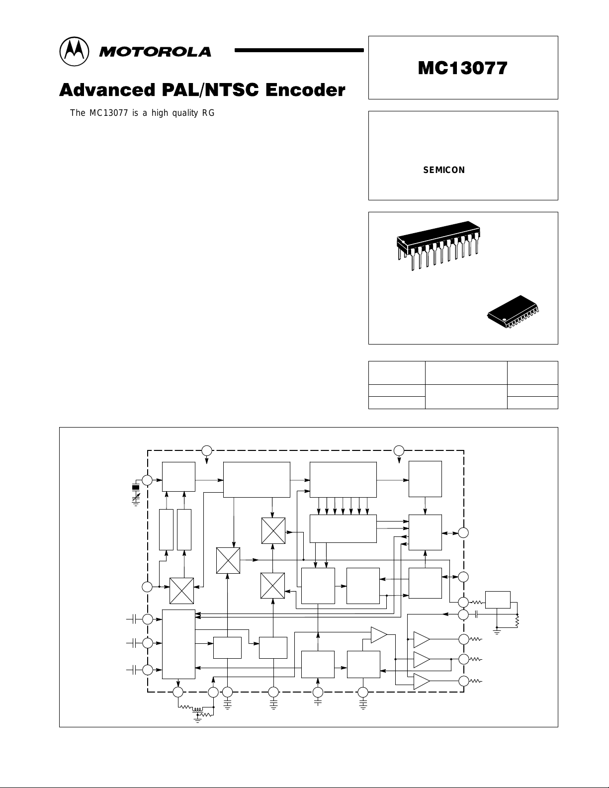
The MC13077 is a high quality RGB/YUV to NTSC/PAL encoder with
Composite Video and S–Video outputs. The IC integrates the color
difference and luma matrix circuitry, chroma modulators, subcarrier
oscillator, and logic circuitry to encode component video into a composite
video signal compatible with the NTSC/P AL standards. The IC operates off a
standard + 5.0 V supply and typically requires less than 75 mA, making it
useful in PC environments. The high degree of integration saves board
space and cost, as only passive external components are required for
operation. The IC is manufactured using Motorola’s MOSAIC process and
is available in a 20 pin DIP or SOIC package.
• Single 5.0 V Supply
• Composite Output
• S–Video Outputs
• P AL/NTSC Switchable
• P AL Squarewave Output
• P AL Sequence Resettable
• Internal/External Burst Flag
• Digitally Determined Modulator Axes
• Subcarrier Reference Drive Selectable
Order this document by MC13077/D
ADVANCED
PAL/NTSC ENCODER
SEMICONDUCTOR
TECHNICAL DATA
20
1
DW SUFFIX
PLASTIC PACKAGE
CASE 751D
(SO–20L)
PLASTIC PACKAGE
20
P SUFFIX
CASE 738
1
4x fsc Xtal/
4x fsc Input
14.32/
17.73
20 p
3.58/4.43 MHz
In/ PLL Off
Red In
1.0
µ
Green In
1.0
µ
Blue In
1.0
µ
12
13
14
V
CC
1
4x f
sc
Oscillator
8
45
PLL
LPF
Off
9
Color
Difference
Y
out
R–Y
and
B–Y
Luma
Matrix
Sync
Y
in
10 15 16
Luma Delay
1.2 k
1.2 k
°
R–Y Burst Flag
B–Y Burst Flag
B–Y
Clamp
Simplified Block Diagram
Divide by Four
Ring Counter
0
°
B–Y
Clamp
90
R–Y
Clamp
°
R–Y
Clamp
H/2
R
H
sync
Latch
Sync
Input
Divide by 512
Countdown
Decoder
H
Luma
Clamp
Sync In/
Sync Sep
MC13077DW
MC13077P
PAL
F/F
576
Luma
Clamp
ORDERING INFORMATION
Operating
Device
Gnd
11
Temperature Range
TA = 0° to +70°C
3.58/
4.43
Latch
Burst
Flag
Adjust
PAL/
NTSC
Switch
Chroma Out
Chroma In
18
19
17
20
4
3
2
Plastic DIP
Burst Flag
Out/Force Burst
Flag
PAL Squarewave
Out/ Force NTSC
Chroma
1.0 k
BPF
4.7 n
Chroma
75
S–Video
Luma
S–Video
75
Comp
Video
75
Package
SO–20L
1.1 k
MOTOROLA ANALOG IC DEVICE DATA
Motorola, Inc. 1996 Rev 2
1
MC13077
MAXIMUM RATINGS
Rating Symbol Value Unit
Supply Voltage V
Storage Temperature T
Operating Junction Temperature T
Operating Ambient Temperature T
CC
stg
J
A
RECOMMENDED OPERATING CONDITIONS
Characteristic Min Typ Max Unit
Supply Voltage 4.5 5.0 5.5 Vdc
Sync Input Threshold Equivalent (See Figure 2) – 1.4 – Vdc
Pulse Width – 4.5 – 5.5 – µs
R, G, B Input (Amplitude for 100% Saturated Video) – 0.7 – Vpp
R–Y Input Amplitude at Pin 16 (for 100% Saturated Video) – 490 – mVpp
B–Y Input Amplitude at Pin 15 (for 100% Saturated Video) – 350 –
Y Input Amplitude (without sync) at Pins 12, 13, 14 (for 100% Saturated Video) – 700 –
Y Input Amplitude (with sync) at Delay Line – 1.0 – Vpp
External 4x Subcarrier Input to Pin 8 (If crystal is not used) – 300 – mVpp
External Subcarrier Input to Pin 9 – 0.10 to 3.0 – Vpp
Lock Range (with 4x Subcarrier Crystal specified) at Subcarrier Frequency – ± 400 – Hz
Burst Flag Input Threshold (Pin 18) – 2.5 – Vdc
NTSC/PAL Select (Pin 19) Vdc
PAL Switching Amplitude: High – 4.0 –
PAL Switching Amplitude: Low – 1.1 –
NTSC Select Threshold – 0.4 –
6.0 V
– 65 to +150 °C
+150 °C
0 to + 70 °C
ELECTRICAL CHARACTERISTICS (T
Characteristic Pin Min Typ Max Unit
Supply Current (150 Ω Load on Output Pins) 1 55 70 85 mA
Color Burst Amplitude 250 300 350 mVpp
Line–to–Line Burst Amplitude Deviation – 7.0 25 mV
Start after leading edge of Sync: NTSC (3.579 MHz)
Start after leading edge of Sync: PAL (4.43 MHz)
Duration: NTSC (3.579 MHz)
Duration: PAL (4.43 MHz)
PAL Burst Phase: Line n
PAL Burst Phase: Line n+1
NTSC Burst Phase 170 180 190
Subcarrier Leakage in Black
White (100% white)
Composite Video Output (100% saturated output)
Sync Amplitude 240 281 320 mVpp
Line–to–Line Sync Amplitude Deviation (PAL) – 7.0 – mV
Luminance Amplitude Error – – 10 %
Line–to–Line Luminance Amplitude Deviation (PAL) 2 – 3.0 – mVpp
Chrominance Amplitude Error (@ 75 Ω – – 10 %
Line–to–Line Chroma Amplitude Deviation (PAL) load) – < 14 – mVpp
Chrominance Phase Error – – 10 Degrees
Line–to–Line Chrominance Phase Error (PAL) – < 5.0 –
Black Level (RGB at Black during Blanking Intervals) – 500 – mV
Sync Tip Clamp Level above Ground 120 200 280
= 25°C, VCC = 5.0 Vdc, test circuit of Figure 1.)
A
2 & 4
(@ 75 Ω
load)
2 & 4
(@ 75 Ω
load)
–
–
–
–
125
215
–
–
5.0 to 5.3
5.4 to 5.6
9
10
135
225
–
–
–
–
–
–
145
235
25
65
Cycles
Degrees
mV
µs
2
MOTOROLA ANALOG IC DEVICE DATA
MC13077
ELECTRICAL CHARACTERISTICS (continued) (T
= 25°C, VCC = 5.0 Vdc)
A
Characteristic Pin Min Typ Max Unit
Luma S–Video Output
Sync Amplitude 240 281 320 mVpp
Line–to–Line Sync Amplitude Deviation (PAL) 3 – 7.0 – mV
Luminance Amplitude Error (@ 75 Ω – – 10 %
Line–to–Line Luminance Amplitude Deviation (PAL) load) – 3.0 – mVpp
Black Level – 500 – mV
Sync Tip Clamp Level above Ground 120 200 280
Chroma S–Video Output
Chrominance Amplitude Error – – 10 %
Line–to–Line Chrominance Amplitude Deviation (PAL) 4 – < 14 – mVpp
Chrominance Phase Error (@ 75 Ω – – 10 Degrees
Black Level load) – 500 – mV
Figure 1. T est Circuit
G
1.0 µF
V
CC
1
4x Subcarrier In
1.0
µ
R
1.0
µ
G
1.0
µ
B
4x f
8
9
12
13
14
sc
Oscillator
45
°
PLL
LPF
Off
R–Y Burst Flag
B–Y Burst
Color
Difference
and
Luma
Matrix
10 15 16
Y
out
1.2 k
R–Y
B–Y
Sync
Luma Delay
1.2 k
Flag
Y
Clamp
in
Divide by Four
Ring Counter
0
°
B–Y
(B–Y) In
10 nF
90
R–Y
Clamp
°
H/2
(R–Y) In
10 nF
R
H
sync
Latch
Sync
Input
Sync In/
Sync Sep
Divide by 512
Countdown
Decoder
H
F/F PAL
Clamp
10 nF
Luma
576
Luma
Clamp
11
3.58/4.43
Switch
Ground
Latch
Burst
Flag
Adjust
PAL/
NTSC
Chroma Out
Chroma In
Burst Flag Out/
18
Force Burst Flag
PAL Squarewave
19
Out/Force NTSC
1.0 k
17
20
4
3
2
Chroma
1.0 nF
75
75
75
BPF
75
75
75
Chroma
S–Video
Luma
S–Video
Comp
Video
1.1 k
MOTOROLA ANALOG IC DEVICE DATA
3
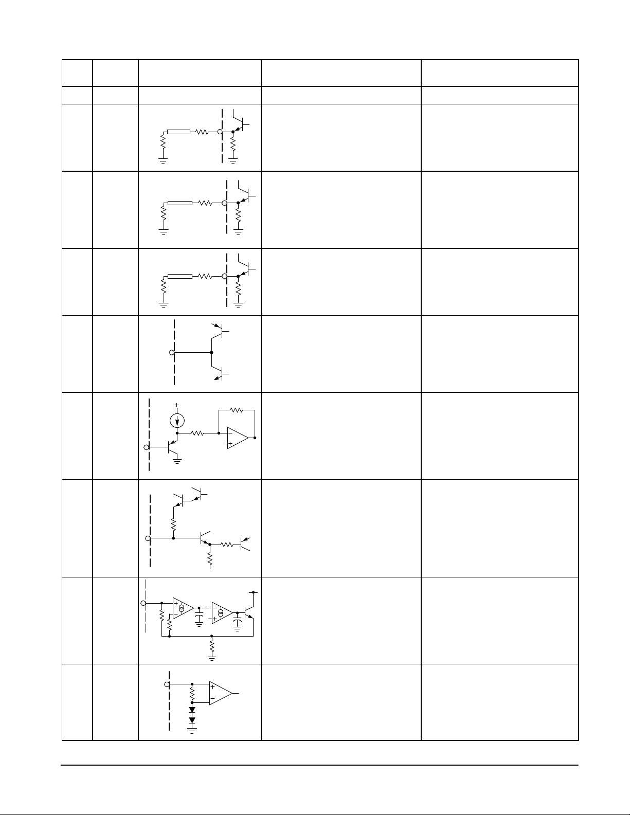
Pin Symbol
1 V
CC
2 Comp
Video
Internal Equivalent
Schematic
Zo = 75
75
Ω
Ω
75
MC13077
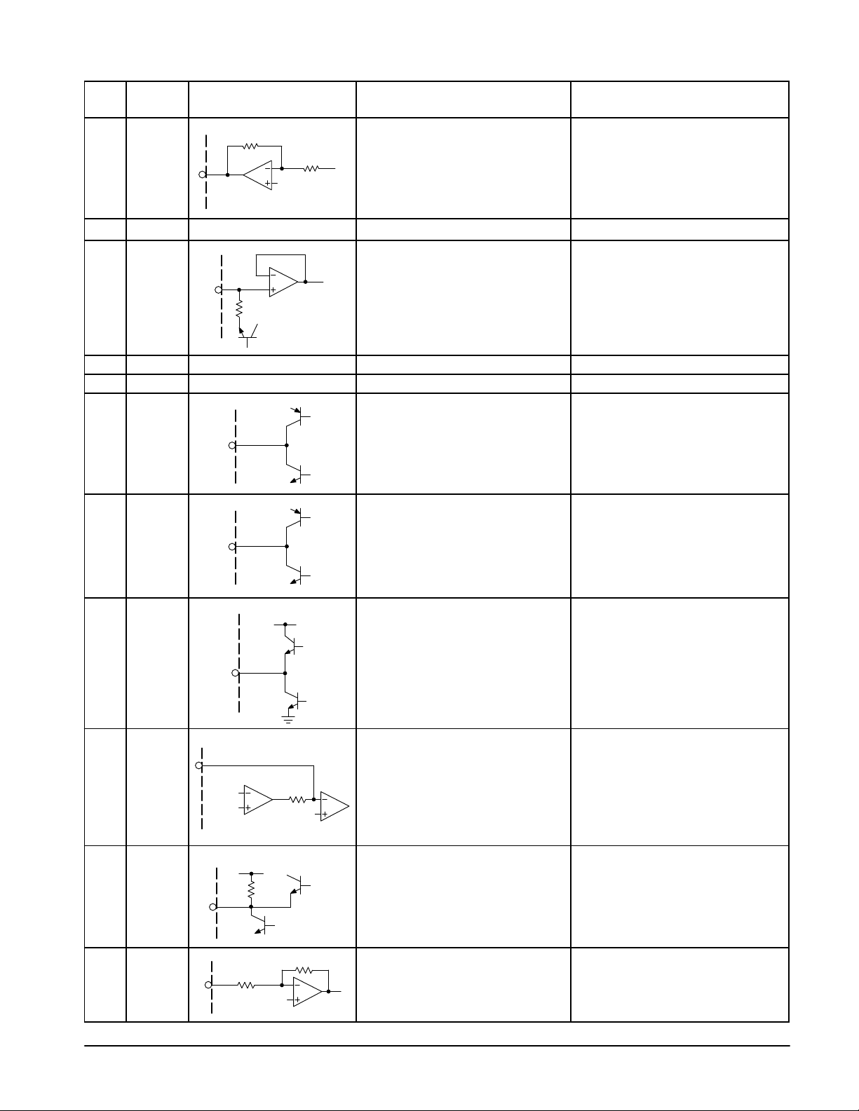
PIN DESCRIPTIONS
Description Expected Waveforms
Supply Voltage + 5.0 Vdc ±10%
Composite Video output. The external
75 Ω series resistor determines the
impedance of the output. The output will
Ω
1.0
drive a 75 Ω load through a 75 Ω coax.
Ω
k
1.0 Vpp (75% Color Saturation),
1.23 Vpp (100% Color Saturation) at
the 75 Ω load.
3 Luma
S–Video
4 Chroma
S–Video
5 Luma
Clamp
6 Y
In
75
75
Ω
Ω
Zo = 75
Zo = 75
Luminance S–Video output. The external
Ω
75
Ω
Ω
75
Ω
1.4 V
75 Ω series resistor determines the
impedance of the output. The output will
drive a 75 Ω load through a 75 Ω coax.
1.0
Ω
k
Chrominance S–Video output. The
external 75 Ω series resistor determines
the impedance of the output. The output
1.0
will drive a 75 Ω load through a 75 Ω
Ω
k
coax.
Luminance Output Clamp storage
capacitor. A 0.01 µF capacitor should be
connected from this pin to ground.
Luminance input from the delay line. The
delayed Luma from Pin 10 is applied at
this pin.
1.0 Vpp with sync (100% output) at the
75 Ω load.
885 mVpp (100% output) when at the
75 Ω load.
3.4 Vdc.
500 mVpp of Composite Luma when
100% saturated RGB inputs are applied.
7 Sync In/
Sync Sep
8 4x fsc Xtal
/4x fsc In
9 3.58/
4.43 MHz
In/PLL Off
4
10 k
400
10 k
gm
V
ref
2.0 V
gm
2.0 k
Composite Sync input. Negative going
sync should be applied at this pin. The
input has a threshold of 1.4 V .
V
Four times Subcarrier Frequency Crystal
CC
Oscillator pin. This pin provides for the
connection of the oscillator resonant
element. Pin may also be driven directly
with a 4x subcarrier signal.
External Subcarrier Input. This pin
provides an input to a Phase Detector and
PLL and allows phase–lock of the 4x
oscillator to an external subcarrier
reference. To disable the PLL, this pin
should be grounded. 400 Hz of pull–in and
lock–in range is possible with a crystal.
The peak voltage may not exceed VCC.
Minimum voltage should not be less than
0 V . See Figure 2 for input requirements.
300 to 600 mVpp 4x subcarrier input if
the pin is being externally driven.
Approximately 40 mVpp, if a crystal is
being used.
0.10 to 3.0 Vpp (AC coupled) of
subcarrier to phase–lock 4x oscillator or
grounded to disable the PLL.
MOTOROLA ANALOG IC DEVICE DATA
MC13077
PIN DESCRIPTIONS (continued)
Internal Equivalent
Pin Symbol
10 Y
Out
11 Gnd Ground Ground
12 Red
13 Green
14 Blue
15 B–Y
16 R–Y
In
In
In
Clamp
Clamp
Schematic
10 k
10 k
1.4 V
20 k
V
ref
See Pin 12 Green Video input. 0.7 Vpp AC coupled (100% Color Bars).
See Pin 12 Blue Video input. 0.7 Vpp AC coupled (100% Color Bars).
Luminance Delay Line Drive Output. A
delay should be inserted between this
pin and Pin 6 to match the delay incurred
by the Chroma.
Red Video input. 0.7 Vpp AC coupled (100% Color Bars).
B–Y Clamp storage capacitor. A 0.01 µF
capacitor should be connected from this
pin to ground, unless the pin is used as
an input.
R–Y Clamp storage capacitor. A 0.01 µF
capacitor should be connected from this
pin to ground, unless the pin is used as
an input.
Description Expected Waveforms
1.0 Vpp with sync
(100% saturated Color Bar output).
If not used as an input the pin is clamped
during sync to 2.4 Vdc. Can be used as a
B–Y input (AC coupled, 350 mVpp, 100%
color saturation). Burst Flag, if disabled
at Pin 18, must be inserted here with the
following signal levels; –170 mV (NTSC),
–121 mV (PAL).
If not used as an input the pin is clamped
during sync to 2.4 Vdc. Can be used as a
R–Y input (AC coupled, 490 mVpp, 100%
color saturation). Burst Flag, if disabled
at Pin 18, must be inserted here with the
following signal level; +121 mV for PAL.
17 Chroma
Out
18 Burst Flag
Out/Force
Burst Flag
19 PAL
Square–
wave
Out/Force
NTSC
20 Chroma
In
Internal
Burst
Flag
V
CC
10 k
V
1/2 V
2.0 V
CC
10 k
CC
10 k
1.4 V
Chroma Bandpass Drive Output. 2.8 Vpp (100% Color Bars)
Burst Flag Output Disable and Force pin.
If left unconnected, internally generated
color burst will appear at Pins 2 and 4.
Burst Flag will appear at this pin (18). If
grounded, the Burst Flag will be
disabled. If externally driven from
another source of burst flag, the internal
flags will be overriden.
PAL/NTSC system switch. If grounded,
the MC13077 will encode NTSC, and if
left open, PAL.
Chroma Bandpass input. Output from
chroma bandpass filter should be
applied at this pin.
1.8 Vpp burst flag pulses if unconnected.
In PAL mode, a PAL squarewave
appears at this pin, the phase of which
can be reset by momentarily forcing the
pin to ground during the high state of
the squarewave.
1.4 Vpp (100% Color Bars) with
bandpass filter and 1.0 kΩ matching
resistors.
MOTOROLA ANALOG IC DEVICE DATA
5
 Loading...