

Device
Operating
Temperature Range
Package
SEMICONDUCTOR
TECHNICAL DATA
MINI–WATT
AUDIO OUTPUT
ORDERING INFORMATION
MC13060D TA = – 40 to +85°C SOP–8
Order this document by MC13060/D
D SUFFIX
PLASTIC PACKAGE
CASE 751
(SOP–8)
8
1
PIN CONNECTIONS
Power Type
Lead Frame
Output
Gnd
V
CC
Feedback
Gnd
Input
(Top View)
1
2
3
4
8
7
6
5
1
MOTOROLA ANALOG IC DEVICE DATA
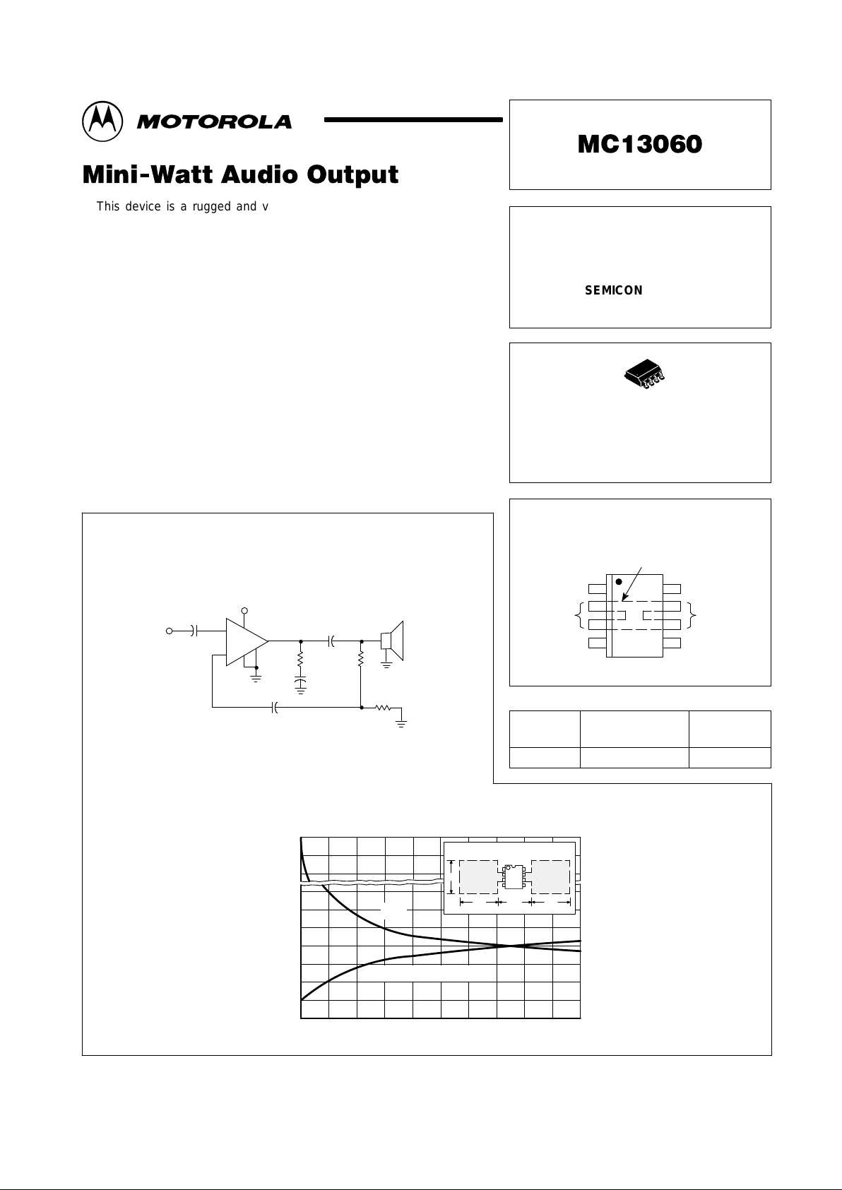
This device is a rugged and versatile power amplifier in a remarkable
plastic power package.
• Supply Voltages from 6.0 Vdc to 35 Vdc
• 2.0 W Output @ 70°C Ambient on PC Board with Good
Copper Ground Plane
• Self Protecting Thermal Shutdown
• Easy to Apply, Few Components
• Gain Externally Determined
• Output is Independent of Supply V oltage Over a Wide Range
Figure 1. Simplified Application
Figure 2. Thermal Resistance & Maximum Power Dissipation
versus PC Board Copper
R , JUNCTION-TO-AIR ( C/W)
°
θ
JA
L
L L9mm
PC Board Heatsink Example
P , MAXIMUM POWER DISSIP ATION (W)
D
1.0µF
Audio
Input
+
VCC = 6.0V to 35V
5
8
4
1
6, 7
2, 3
47
µ
F
+
+
–
0.1
100
µ
F
+
330
6.8
V
out
Speaker
16/32
Ω
3.0
160
140
60
40
20
0
L, LENGTH OF COPPER
01020304050
3.0
2.0
1.0
0
2.0 oz.
Copper
R
θ
JA
P
D(max)
for TA = 70°C
Motorola, Inc. 1996 Rev 0
MC13060
2
MOTOROLA ANALOG IC DEVICE DATA
MAXIMUM RATINGS
Rating Symbol Value Unit
Power Supply Voltage V
CC
35 V
Audio Input, Pin 5 1.0 V
pp
Thermal Resistance, Junction to Air R
θJA
160 °C/W
Thermal Resistance, Junction to Case R
θJC
25 °C/W
Junction Temperature T
J
150 °C
Operating Ambient Temperature Range T
A
–40 to +85 °C
Storage Temperature Range T
stg
–65 to +150 °C
ELECTRICAL CHARACTERISTICS (T
A
= 25°C, circuit of Figure 3, unless otherwise noted.)
Characteristics
Symbol Min Typ Max Unit
AUDIO SECTION
Power Supply Current, No Signal I
CC
– 13 – mAdc
Gain A
o
– 50 – V/V
Distortion at 62.5 mW Output, 1.0 kHz THD – 0.2 1.0 %
Distortion at 900 mW Output, 1.0 kHz THD – 0.5 3.0 %
Quiescent Output Voltage, No Signal V
Pin 1
– 8.4 – Vdc
Input Bias V
Pin 5
, V
Pin 8
– 0.7 – Vdc
Input Resistance Rin, Pin 5 – 28 – kΩ
Output Noise (50 Hz to 15 kHz) Input 50 Ω V
out
– 0.5 4.0 mVrms
GENERAL DESCRIPTION
The MC13060 is a quasi–complementary audio power
amplifier, mounted in the SOP 8 (power SOIC package). It is
well suited to a variety of 1.0 W and 2.0 W applications in
radio, TV, intercom, and other speaker driving tasks. It
requires the usual external components for high frequency
stability and for gain adjustment.
The output signal voltage and the power supply drain
current are very linearly related, as shown in Figure 5. Both
are quite constant over wide variation of the power supply
voltage (above minimum VCC for clipping, of course). The
amplifier can best be described as a voltage source with
about 1.0 App capability. On a good heatsink, it can deliver
over 2.0 W at 70°C ambient.
The MC13060 will automatically go into shutdown at a die
temperature of about 150°C, effectively protecting itself, even
on fairly stiff power supplies. This eliminates the need for
decoupling the power supply, which degrades performance
and requires extra components.
Input Pins 5 and 8 are internally biased at 0.7 Vdc and
should not be driven below ground.
4
Audio Input
16
Ω
Load
1.0
µ
F
+
I
CC
5
8
1
6, 7
2, 3
47
µ
F
+
+
–
3.0
0.1
100
µ
F
+
330
6.8
50
VCC = +16Vdc
Figure 3. Test Circuit

MC13060
3
MOTOROLA ANALOG IC DEVICE DATA
16 V
32 Ω Load
VCC = 32 V
28 V
1 %
THD
24 V
20 V
400 Hz
Signal
16 V/16
Ω
24 V/32
Ω
24 V/16
Ω
32 V/32
Ω
CC
I , SUPPLY CURRENT (mAdc)
All Curves Taken in the Test Circuit of Figure 3, Unless Otherwise Noted.
Figure 4. Quiescent Supply Current and
Output Voltage versus Supply Voltage
Figure 5. Supply Current versus Output
Figure 6. Distortion and Gain versus Frequency Figure 7. Distortion versus Power Output
Figure 8. Dissipation versus Output Power Figure 9. Dissipation versus Output Power
AVG. OUTPUT VOLTAGE (Vdc)
VCC, SUPPLY VOLTAGE (Vdc)
0 10203040
I , SUPPLY CURRENT (mAdc)
CC
SINE WAVE OUTPUT VOLTAGE (Vrms)
0 1.0 2.0 3.0 4.0 5.0 6.0 7.0 8.0
PO, POWER OUTPUT (W)
1.0 2.0
0
THD, TOT AL HARMONIC DISTORTION (%)
RELATIVE GAIN (dB)
f, FREQUENCY (Hz)
10 100 1.0 k 10 k
P
D
PO, POWER OUTPUT (W)
1.0 2.0
THD, TOT AL HARMONIC DISTORTION (%)
PO, POWER OUTPUT (W)
0.1 1.0 2.0 10
, POWER DISSIPATION (V)
P
D
, POWER DISSIPATION (V)
12
10
20
18
16
14
8.0
6.0
4.0
2.0
0
200
180
160
140
120
100
80
60
40
20
0
0
2.0
1.0
2.0
1.8
1.6
1.4
1.2
1.0
0.8
0.6
0.4
0.2
0
2.0
1.0
0
2.0
1.6
1.4
1.2
1.0
0.8
0.6
0.4
0.2
0
1.8
4.0
2.0
1.0
0
–1.0
–2.0
–3.0
–4.0
–5.0
–6.0
3.0
Signal = 0
I
CC
VO (DC)
RL = 16
Ω
VCC = 24 V
RL = 32
Ω
VCC = 32 V
RL =∞, VCC = 32 V
VCC = 16 V, RL = 16 Ω, 0.5 W
Gain
THD
16 Ω Load
VCC = 24 V
1% THD
20 V
16 V

MC13060
4
MOTOROLA ANALOG IC DEVICE DATA
Figure 10. Representative Schematic Diagram
Audio
Input
Audio
Feedback
Audio V
CC
Audio
Output
Ground
Pins
R5
1.3kR61.3k
R8
110
R9
5.1k
R10
62
8
D3
Q5
Q6 Q9
Q11
5D2
Q10
Q12 Q13
Q7
R7
28k
Q1
R1
13k
R3
4.6k
R4
4.6k
Q3 Q4
Q2
R2
13k
C1
5.0pF
30k
Q14
4
1
Q15
Q18
Q18A
D1
Q16 R14
140
Q19
Q20
Q22
Q23
Q17
R13
33k
R15
330
30k
Q21
C2
15pF
Q8
2, 3
5, 6

MC13060
5
MOTOROLA ANALOG IC DEVICE DATA
D SUFFIX
PLASTIC PACKAGE
CASE 751–05
(SOP–8)
ISSUE N
OUTLINE DIMENSIONS
NOTES:
1. DIMENSIONING AND TOLERANCING PER
ANSI Y14.5M, 1982.
2. CONTROLLING DIMENSION: MILLIMETER.
3. DIMENSIONS A AND B DO NOT INCLUDE
MOLD PROTRUSION.
4. MAXIMUM MOLD PROTRUSION 0.15 (0.006)
PER SIDE.
5. DIMENSION D DOES NOT INCLUDE DAMBAR
PROTRUSION. ALLOWABLE DAMBAR
PROTRUSION SHALL BE 0.127 (0.005) TOTAL
IN EXCESS OF THE D DIMENSION AT
MAXIMUM MATERIAL CONDITION.
SEATING
PLANE
14
58
C
K
4X P
A0.25 (0.010)MTB
SS
0.25 (0.010)MB
M
8X D
R
M
J
X 45
_
_
F
–A–
–B–
–T–
DIM MIN MAX MIN MAX
INCHESMILLIMETERS
A 4.80 5.00 0.189 0.196
B 3.80 4.00 0.150 0.157
C 1.35 1.75 0.054 0.068
D 0.35 0.49 0.014 0.019
F 0.40 1.25 0.016 0.049
G 1.27 BSC 0.050 BSC
J 0.18 0.25 0.007 0.009
K 0.10 0.25 0.004 0.009
M 0 7 0 7
P 5.80 6.20 0.229 0.244
R 0.25 0.50 0.010 0.019
____
G

MC13060
6
MOTOROLA ANALOG IC DEVICE DATA
Motorola reserves the right to make changes without further notice to any products herein. Motorola makes no warranty , representation or guarantee regarding
the suitability of its products for any particular purpose, nor does Motorola assume any liability arising out of the application or use of any product or circuit, and
specifically disclaims any and all liability, including without limitation consequential or incidental damages. “T ypical” parameters which may be provided in Motorola
data sheets and/or specifications can and do vary in different applications and actual performance may vary over time. All operating parameters, including “Typicals”
must be validated for each customer application by customer’s technical experts. Motorola does not convey any license under its patent rights nor the rights of
others. Motorola products are not designed, intended, or authorized for use as components in systems intended for surgical implant into the body, or other
applications intended to support or sustain life, or for any other application in which the failure of the Motorola product could create a situation where personal injury
or death may occur. Should Buyer purchase or use Motorola products for any such unintended or unauthorized application, Buyer shall indemnify and hold Motorola
and its officers, employees, subsidiaries, affiliates, and distributors harmless against all claims, costs, damages, and expenses, and reasonable attorney fees
arising out of, directly or indirectly, any claim of personal injury or death associated with such unintended or unauthorized use, even if such claim alleges that Motorola
was negligent regarding the design or manufacture of the part. Motorola and are registered trademarks of Motorola, Inc. Motorola, Inc. is an Equal
Opportunity/Affirmative Action Employer.
How to reach us:
USA/EUROPE / Locations Not Listed: Motorola Literature Distribution; JAPAN: Nippon Motorola Ltd.; Tatsumi–SPD–JLDC, 6F Seibu–Butsuryu–Center,
P.O. Box 20912; Phoenix, Arizona 85036. 1–800–441–2447 or 602–303–5454 3–14–2 Tatsumi Koto–Ku, Tokyo 135, Japan. 03–81–3521–8315
MFAX: RMF AX0@email.sps.mot.com – TOUCHT ONE 602–244–6609 ASIA/PACIFIC: Motorola Semiconductors H.K. Ltd.; 8B Tai Ping Industrial Park,
INTERNET: http://Design–NET.com 51 Ting Ko k Road, Tai Po, N.T ., Hong Kong. 852–26629298
MC13060/D
*MC13060/D*
◊
 Loading...