

Motorola MC13030DW Datasheet
Device
Operating
Temperature Range
Package
SEMICONDUCTOR
TECHNICAL DATA
DUAL CONVERSION
AM RECEIVER
ORDERING INFORMATION
MC13030DW TA = –40° to +85°C SOIC–28
DW SUFFIX
PLASTIC PACKAGE
CASE 751F
28
1
(Top View)
PIN CONNECTIONS
Order this document by MC13030/D
1
2
3
4
5
6
7
8
9
10
11
12
13
14
28
27
26
25
24
23
22
21
20
19
18
17
16
15
Mix1 In
Mix1 In
RF Gnd
FET RF AGC
RF AGC2
RF AGC Adj
Mix1 RF AGC Adj
SD Level
IF Gnd
SD IF Out
S Level Out
IF AGC In
AF Out
V
CC
VCO Out
VCO
VCO Ref
Mix1 Out
Mix1 Out
V
ref
Mix2 In
Mix2 Out
Mix2 Out
Xtal Osc E
Xtal Osc B
IF In
Det V
ref
Det In
1
MOTOROLA ANALOG IC DEVICE DATA
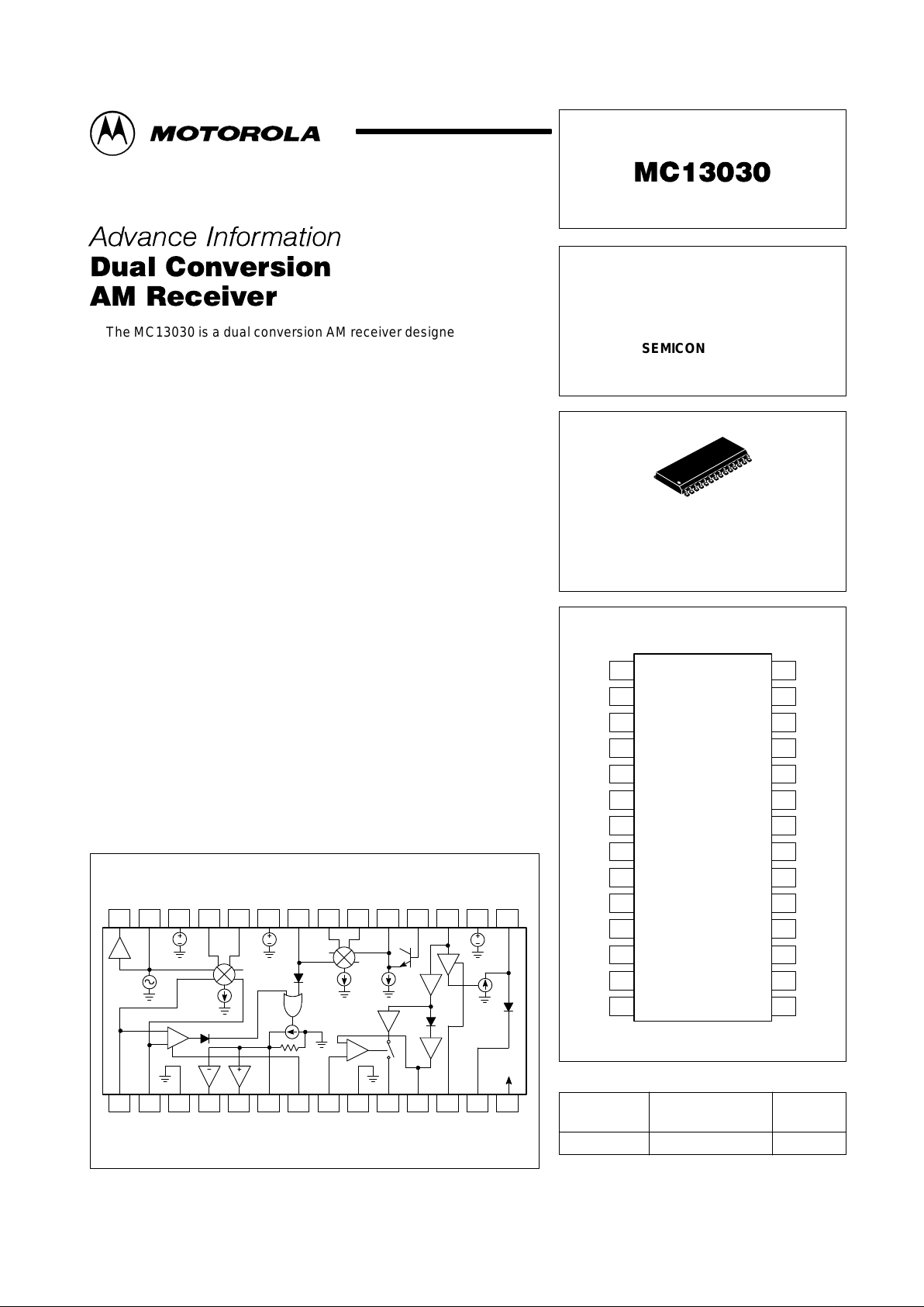
The MC13030 is a dual conversion AM receiver designed for car radio
applications. It includes a high dynamic range first mixer, local oscillator,
second mixer and second oscillator, and a high gain AGC’d IF and
detector. Also included is a signal strength output, two delayed RF AGC
outputs for a cascode FET/bipolar RF amplifier and diode attenuator, a
buffered IF output stage and a first local oscillator output buf fer for driving
a synthesizer . Frequency range of the first mixer and oscillator is 100 kHz
to 50 MHz.
Applications include single band and multi–band car radio receivers, and
shortwave receivers.
• Operation from 7.5 to 9.0 Vdc
• First Mixer, 3rd Order Intercept = 20 dBm
• Buffered First Oscillator Output
• Second Mixer, 3rd Order Intercept = +5.0 dBm
• No Internal Beats Between 1st and 2nd Oscillator Harmonics
• Signal Strength Output
• Limited 2nd IF Output for Frequency Counter Station Detector
• Adjustable IF Output Station Detector Level
• Adjustable RF AGC Threshold for Both Mixer Inputs
• Two Delayed AGC Outputs for Cascode RF Stage and Diode Attenuator
Representative Block Diagram
This device contains 335 active transistors.
1413121110987654321
1516171819202122232425262728
V
CC
VCO
5.1 V 6.5 V
Mix1
Mix2 XTal
Osc
4.1 V
3.0 mA
IF Amp
AGC
6.6 mA
Motorola, Inc. 1996 Rev 1
MC13030
2
MOTOROLA ANALOG IC DEVICE DATA
MAXIMUM RATINGS (T
A
= 25°C, unless otherwise noted.)
Rating
Symbol Value Unit
Power Supply V
CC
10 V
Operating Temperature T
A
–40 to +85 °C
Storage Temperature T
stg
–65 to +150 °C
Junction Temperature T
J
150 °C
NOTE: ESD data available upon request.
ELECTRICAL CHARACTERISTICS (T
A
= 25°C, VCC = 8.0 V, unless otherwise noted.)
Characteristic
Condition/Pin Symbol Min Typ Max Unit
Power Supply Voltage – V
CC
7.5 8.0 9.0 V
Power Supply Current VCC = 8.0 V I
CC
26 32 44 mA
Detector Output Level Vin = 1.0 mV , 30% Mod. V13 160 200 240 mVrms
Audio S/N Ratio Vin = 1.0 mV , 30% Mod. S/N 48 52 – dB
Audio THD Vin = 1.0 mV , 30% Mod.
THD – 0.3
1.0
%
Vin = 1.0 mV , 80% Mod.
– 0.3
1.0
Vin = 2.0 mV , 80% Mod. – 0.4 1.5
Signal Strength Output Vin = 0 to 2.0 V V11 0 – 5.2 V
VCO Buffer Output – V28 178 224 282 mV
SD Output Level Vin = 1.0 mV , V11 > V8 V10 2.3 2.7 3.3 Vpp
MIXER1
Input Resistance 1 or 2 to Gnd – – 10 – kΩ
Third Order Intercept Point 1 or 2 IP3 – 127 – dBµV
Conversion Transconductance 1 or 2 to 24 + 25 g
c
– 2.2 – mS
Total Collector Current 24 + 25 I
C
– 4.6 – mA
Input IF Rejection 1 or 2 – – 45 – dB
MIXER2
Input Resistance 22 – – 2.4 – kΩ
Third Order Intercept Point 22 IP3 – 112 – dBµV
Conversion Transconductance 22 to 20 + 21 g
c
– 4.6 – mS
Total Collector Current 20 + 21 I
C
– 3.0 – mA
VCO
Minimum Oscillator Coil Parallel Impedance 27 to 26 R
P
– 3.0 – kΩ
Buffer Output Level 28 V
O
– 224 – mVrms
Stray Capacitance 27 C
S
– 7.0 – pF
IF AMPLIFIER
Input Resistance 17 R
in
– 2.0 – kΩ
Transconductance 17 to 15 g
m
– 28 – mS
Maximum Input Level 17 V
in
– 125 – mVrms
Minimum Detector Coil Parallel Impedance 17 to 15 R
L
– 15 – kΩ
RF Output Level 15, Vin = 1.0 mV – – 2.0 – Vpp
Audio Output Impedance 13 R
out
– 120 – Ω
Audio Output Level 13 @ 30% Mod. V
out
– 200 – mVrms
MC13030
3
MOTOROLA ANALOG IC DEVICE DATA
NOTES: 1. The transformers used for at the output of the mixers are wideband 1:4 impedance ratio. The secondary load is the 50 Ω input of the spectrum
analyzer, so the impedance across the collectors of the mixer output is 200 Ω.
2.Since the VCO frequency is not critical for this measurement, a fixed tuned oscillator tuned to 11.7 MHz is used. This gives an input frequency
of 1.0 MHz.
3.The detector coil is loaded with a 10 k resistor to reduce the tuned circuit Q and to present a 10 kΩ load to the IF output for determination of IF
transconductance.
4.The RF AGC current, S output current and Pin 6 current are measured by connecting a current measuring meter to these pins, so they are effectively
shorted to ground.
5.SD adjust is adjusted by connecting a power supply or potentiometer and voltmeter to Pin 8.
Figure 1. Test Circuit
1516171819202122232425262728
VCO
Out
VCO VCO
Ref
Mix1
Out
Mix1
OutRFV
ref
Mix2InMix2
Out
Mix2
Out
Xtal
Osc E
Xtal
Osc B
IF In Det
V
ref
Det
In
Mix1InMix1InRF
Gnd
FET
RF
AGC
RF
AGC2
RF
AGC
Adj
Mix1
RF AGC
Adj
SD
LevelIFGnd
SD IF
Out
S Level
OutIFAGC InAFOut
V
CC
Mixer1 Out Mixer2 Out
8.0 V
Mixer2 In
Osc Out
Mixer1 Input
FO = 1.0 MHz
FET RF AGC Voltage
RF AGC Current
Pin 6 Current
SD Adjust
IF Signal Out
S Output Current
Audio Out
IF Output/
Det Input
IF
Input
Adj to 11.7 MHz
2.2
µ
H
82 pF
680
µ
H
47
µ
F
8.0 V
10 k 10 k
++
22
0.1
0.1
10.245
47
0.1
1.0
µ
F
+
0.1
0.01
47
47
1:4 1:4
10 k 180 pF
0.1
0.1
R7
0.1
4.7
µ
F
+
1413121110987654321
FUNCTIONAL DESCRIPTION
The MC13030 contains all the necessary active circuits for
an AM car radio or shortwave receiver.
The first mixer is a multiplier with emitter resistors in the
lower, signal input transistors to give a high dynamic range. It
is internally connected to the first oscillator (VCO). The input
pins are 1 and 2. The input can be to either Pins 1 or 2, or
balanced. These pins are internally biased, so a dc path
between them is allowable but not necessary. The mixer
outputs are open collectors on Pins 25 and 26. They are
normally connected to a tuned transformer.
The first oscillator on Pin 27 is a negative resistance type
with automatic level control. The level is low so the signal
does not modulate the tuning diode capacitance and cause
distortion. Pin 26 is the reference voltage for the oscillator
coil. This reference is also the supply for the mixer circuits.
The upper bases of the mixer are 0.7 V below this reference.
The second mixer is similar to the first, but it is single–
ended input on Pin 22. Its outputs are open collectors on
Pins 20 and 21 which are connected to a tuned transformer.
The dynamic range of this mixer is less than the first. It is also
connected internally to an oscillator which is normally crystal
controlled. The oscillator is a standard Colpitts type with the
emitter on Pin 19 and the base on Pin 18.
The IF amplifier input is Pin 17. The AGC operates on the
input stage to obtain maximum dynamic range and minimum
distortion. The IF output, Pin 15, is a current source.
MC13030
4
MOTOROLA ANALOG IC DEVICE DATA
Therefore, its gain is determined by the load impedance
connected between Pins 15 and 16. Pin 16 is a voltage
reference for the output. The output is internally connected to
the AM detector, and Pin 13 is the detector output. This
detector also provides the AGC signal for the IF amplifier. An
RC filter from Pin 13 to 12 removes the audio, leaving a dc
level proportional to the carrier level for AGC.
Pin 11 provides a current proportional to signal strength.
It is a current source so a resistor must be connected from
Pin 11 to ground to select the desired dc voltage range. The
current is proportional to the signal level at Pin 17, the IF
amplifier input.
A high–gain limiting amplifier is used to derive the station
detect (SD) signal output on Pin 10; this output is present only if
it is turned on by the voltage on Pin 8. If the voltage on
Pin 8 is less than the voltage on Pin 11, the output on Pin 10 is
“on”. The station detector IF output on Pin 10 is used with
synthesizers which have a frequency counting signal detector.
The RF AGC outputs on Pins 4 and 5 are controlled by the
signal levels at Mixer1 or Mixer2. Bypass capacitors are
required on Pins 6 and 4 to remove audio signals from the
AGC outputs. Pin 4 is designed to control the NPN transistor
in series with the RF amplifier FET. The voltage on Pin 4 is
5.1 V with no input signal and decreases with increasing input
signal. Pin 5 is designed to control an additional AGC circuit
at the antenna input. The voltage on Pin 5 is at 0 V with no
input signal and increases with increasing input signals. The
voltage on Pin 5 does not increase until the voltage on Pin 4
has decreased to about 1.3 V . In most cases, Pin 5 is used to
drive a diode shunt. Maximum output current is about 850 µA.
The RF AGC sensitivity is about 40 mVrms input to Mixer1
or about 2.0 mVrms input to Mixer2 at 1.0 MHz. The AGC
sensitivity for both mixers can be decreased by adding a
resistor from Pin 6 to ground. There is also an additional
amplifier between Mixer1 and its AGC rectifier. The gain of
this amplifier and AGC sensitivity for Mixer1 can be increased
by adding a resistor from Pin 7 to ground. Therefore, the
desired AGC sensitivity for both mixers can be achieved by
changing the resistors on Pins 6 and 7.
1
2
3
4
5
6
7
8
9
10
11
12
13
14
28
27
26
25
24
23
22
21
20
19
18
17
16
15
Mix1 In
Mix1 In
RF Gnd
FET RF AGC
RF AGC2
RF AGC Adj
Mix1 RF AGC Adj
SD Level
IF Gnd
SD IF Out
S Level Out
IF AGC In
AF Out
V
CC
VCO Out
VCO
VCO Ref
Mix1 Out
Mix1 Out
V
ref
Mix2 In
Mix2 Out
Mix2 Out
Xtal Osc E
Xtal Osc B
IF In
Det V
ref
Det In
Figure 2. Pin Connections and DC Voltages
5.1 V
5.1 V
5.1 V
7.8 V
7.8 V
6.5 V
3.7 V
7.9 V
7.9 V
4.4 V
5.0 V
4.8 V
4.1 V
4.1 V
3.3 V
3.3 V
0 V
5.1 to 0 V
0 to 850
µ
A
0 to 2.8 V
200 mV
43 mV
0 to 4.8 V
0 V
6.5 V
0 to 4.8 V
3.6 to 4.5 V
3.6 to 4.5 V
8.0 V
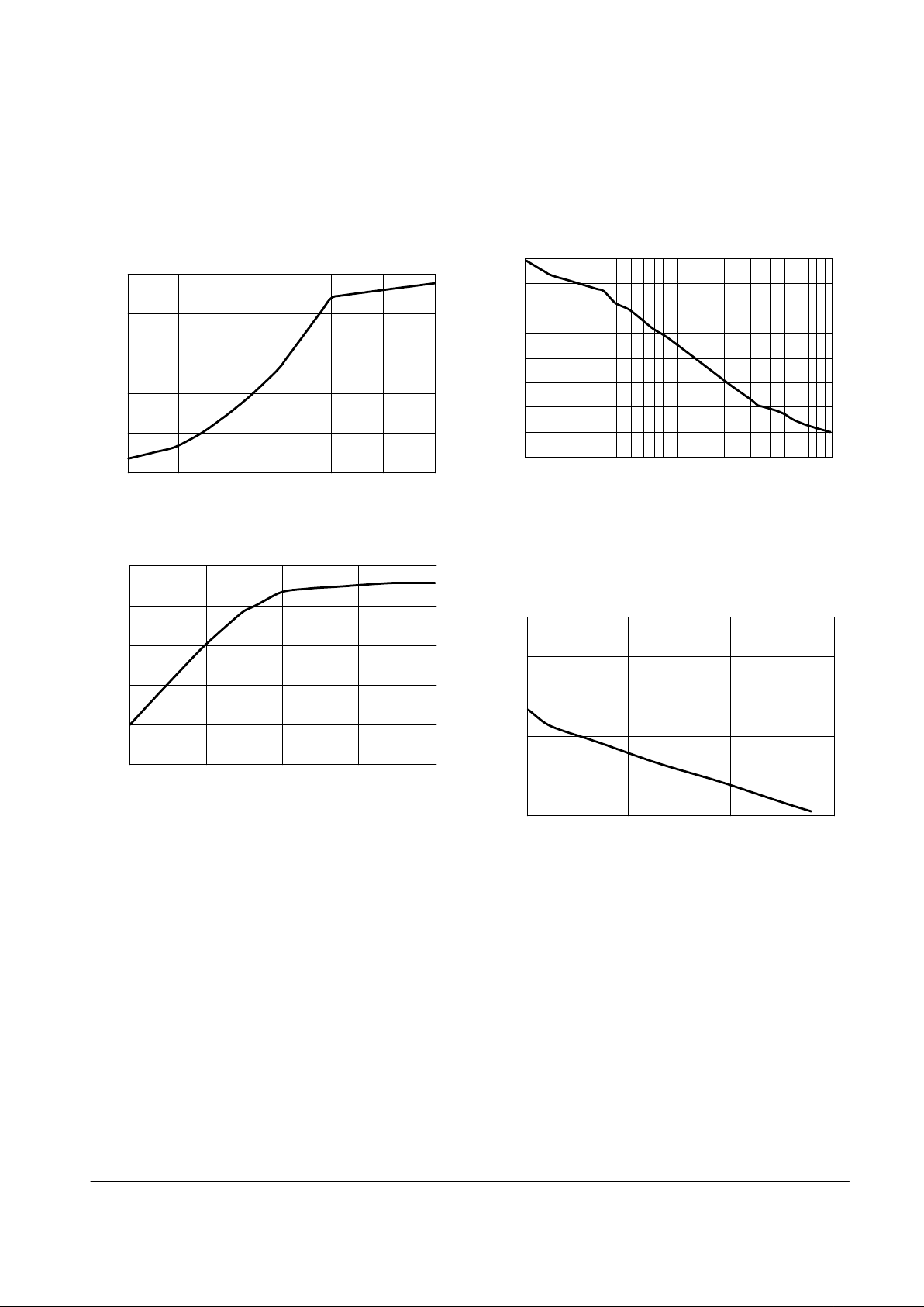
S Out versus IF Input:
The S output current at Pin 11 is provided by two
collectors, one a PNP source and the other a sink to ground.
The desired S output voltage can be selected using the curve
of Figure 3 and calculating the value of the required resistor.
Figure 3. S Output Current versus IF Input Level
IF INPUT LEVEL (dBµV)
30 40 50 100
0
20
40
60
70
PIN 11 CURRENT ( A)
60 70 80 90
µ
RF FET AGC versus Mixer1 and Mixer2 Input Level:
Figures 4 and 5 are generated with no external resistance
on Pins 4 or 6, so they represent the minimum RF AGC
sensitivity of Mixer1 and Mixer2.
Figure 4. RF AGC Voltage versus Mixer1 Input
85 90 95 100 105
0
1.0
2.0
3.0
4.0
5.0
MIXER1 INPUT LEVEL (dB
µ
V)
PIN 4 VOLTAGE (V)
Figure 5. RF AGC Voltage versus Mixer2 Input
MIXER2 INPUT LEVEL (dBµV)
65 70 75 80
0
1.0
2.0
3.0
4.0
5.0
PIN 4 VOLTAGE (V)
MC13030
5
MOTOROLA ANALOG IC DEVICE DATA
Pin 6 Current versus Mixer1 and Mixer2 Input Level:
The internal resistance from Pin 6 to ground is 39 k.
The RF AGC voltage on Pin 4 is 2.0 V when the voltage on
Pin 6 is 1.2 V. Therefore, the desired AGC thresholds for
either mixer can be set with these curves. The design steps
are described in the design notes.
Figure 6. Pin 6 Current versus Mixer1 Input Level
MIXER1 INPUT LEVEL (dBµV)
90 100 110 120
0
50
100
150
200
250
PIN 6 CURRENT ( A)
µ
PIN 6 CURRENT ( A)
µ
Figure 7. Pin 6 Current versus Mixer2 Input Level
MIXER2 INPUT LEVEL (dBµV)
80 90 120
0
50
100
150
200
100 110
250
Mixer1 AGC Gain Increase versus R7:
Adding a resistor from Pin 7 to ground increases the AGC
sensitivity of Mixer1. The range of increase in dB can be
found from this curve. This is useful after setting up the AGC
threshold of Mixer2.
Figure 8. Mixer1 AGC Gain Increase versus R7
R7
100 10 k
0
5.0
6.0
7.0
8.0
INCREASE IN MIXER1 AGC SENSITIVITY (dB)
1.0 k
1.0
2.0
3.0
4.0
Pin 5 Current versus Pin 4 Voltage:
All the curves give Pin 4 AGC voltage versus some other
input level. This curve can be used to determine the auxiliary
AGC current from Pin 5 at a given Pin 4 voltage.
Figure 9. Pin 5 Current versus Pin 4 Voltage
PIN 5 CURRENT (mA)
0 0.4 0.8 1.2
0
1.0
2.0
3.0
4.0
5.0
PIN 4 VOLTAGE
 Loading...