

Motorola MC13028AD, MC13028AP Datasheet
Order this document by MC13028A/D
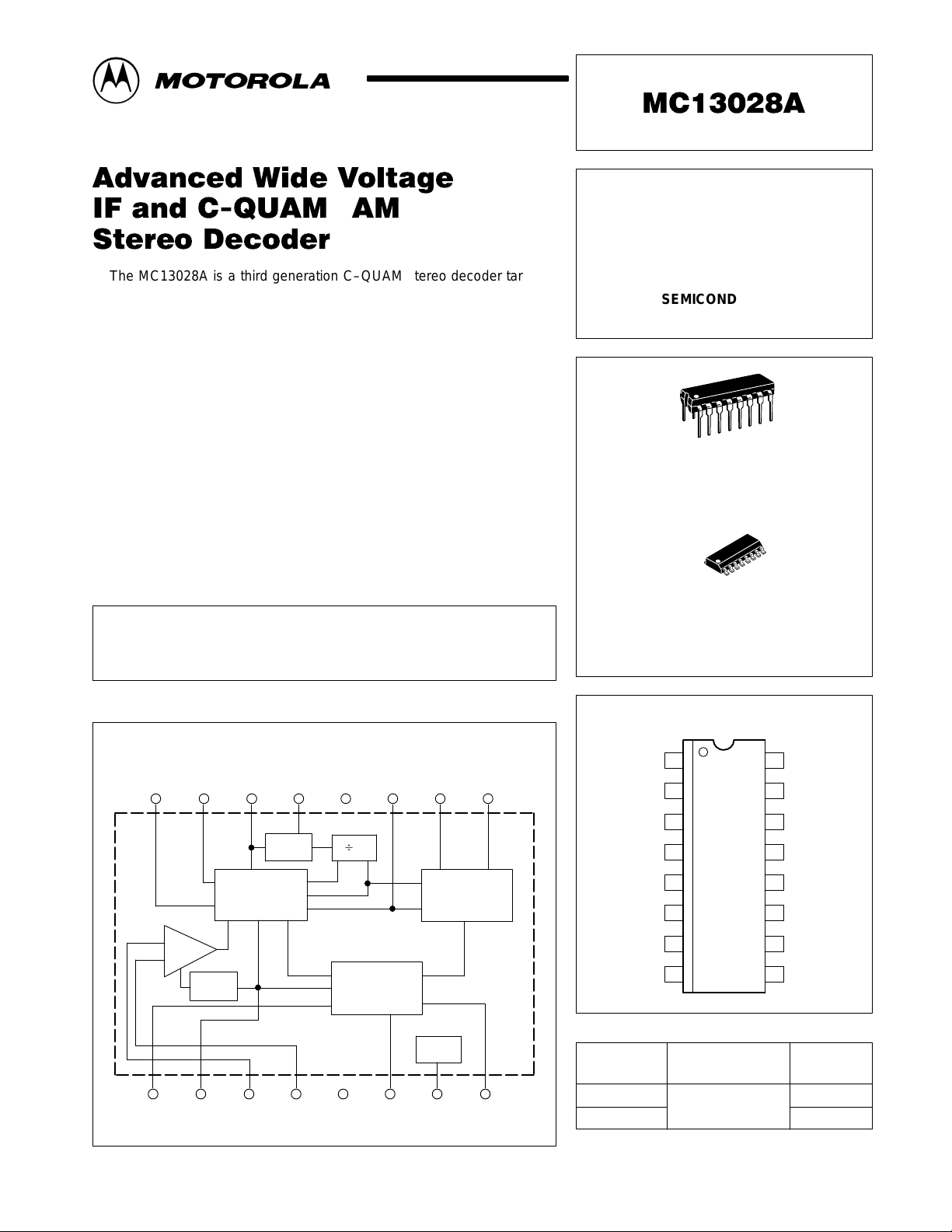
The MC13028A is a third generation C–QUAM stereo decoder targeted
for use in low voltage, low cost AM/FM E.T.R. radio applications. Advanced
features include a signal quality detector that analyzes signal strength,
signal to noise ratio, and stereo pilot tone before switching to the stereo
mode. A “blend function” much like FM stereo has been added to improve
the transition from mono to stereo. The audio output level is adjustable to
allow easy interface with a variety of AM/FM tuner chips. The external
components have been minimized to keep the total system cost low.
• Adjustable Audio Output Level
• Stereo Blend Function
• Stereo Threshold Adjustment
• Operation from 2.2 V to 12 V Supply
• Precision Pilot Tone Detector
• Forced Mono Function
• Single Pinout VCO
• IF Amplifier with IF AGC Circuit
• VCO Shutdown Mode at Weak Signal Condition
The purchase of the Motorola C–QUAMAM Stereo Decoder does not carry with such purchase any license by implication, estoppel or otherwise, under any patent rights of Motorola
or others covering any combination of this decoder with other elements including use in a
radio receiver. Upon application by an interested party, licenses are available from Motorola
on its patents applicable to AM Stereo radio receivers.
C–QUAM AM STEREO
ADVANCED WIDE VOLTAGE
IF and DECODER
for E.T.R. RADIOS
SEMICONDUCTOR
TECHNICAL DATA
16
1
P SUFFIX
PLASTIC PACKAGE
CASE 648
16
1
D SUFFIX
PLASTIC PACKAGE
CASE 751B
(SO–16)
Representative Block Diagram
VCO
AM Stereo
Decoder
IF
Amp
AGC
This device contains 679 active transistors.
B 8
Signal Quality
MOTOROLA ANALOG IC DEVICE DATA
Detector
Pilot Tone
Detector
Reg
PIN CONNECTIONS
Stereo
Filter
Bypass
Gnd
Stereo
1.0 V
Blend
1
2
3
4
5
6
7
8
Threshold Adjust
910111213141516
AGC Bypass
IF Feedback
IF Signal Input
Indicator Drive
Reference
Right Channel
16
Output
Left Channel
15
Output
Loop Filter
14
13
VCO Output
V
12
CC
Pilot Signal
11
Input
Pilot Q Detector
10
Output
Pilot I Detector
9
Output
ORDERING INFORMATION
Operating
Device
87654321
MC13028AD
MC13028AP DIP–16
Motorola, Inc. 1996 Rev 2
Temperature Range
TA = –25° to +70°C
Package
SO–16
1
MC13028A
CC
TA
µ
MAXIMUM RATINGS (
Power Supply Input Voltage
Operating Junction Temperature
Operating Ambient Temperature
Storage Temperature Range
LED Indicator Current
ELECTRICAL CHARACTERISTICS (V
@ 50% Modulation, unless otherwise noted.)
Supply Current Drain
VCC = 2.2 V
VCC = 8.0 V – 11 –
Audio Output Level, L+R, Mono Modulation V
RO = 1.8 k, VCC = 2.2 V, Input 55 dBµV 22 33 44
RO = 10 k, VCC = 8.0 V, Input 50 dBµV 150 200 250
RO = 10 k, VCC = 8.0 V, Input 40 dBµV 80 130 180
RO = 10 k, VCC = 8.0 V, Input 31 dBµV – 50 –
Audio Output Level, L or R Only, Stereo Modulation V
RO = 1.8 k, VCC = 2.2 V, 55 dBµV Input 35 80 106
RO = 10 k, VCC = 8.0 V 340 460 580
Output THD %
50% Stereo, L or R Only THD1 – 0.6 1.8
50% Mono, L+R THD2 – 0.3 0.6
90% Mono, L+R, Input 86 dBµV THD3 – – 1.5
Channel Separation L or R 23 35 – dB
50% L or R Only
Decoder Input Sensitivity V
V
= –10 dB
out
Force to Mono Mode, (Pin 10) – 0.25 0.3 – Vdc
Stereo Threshold Adjust (Pin 1)
Pin 1 Open
R1 = 15 k (Gnd) – 55 –
R1 = 680 k (VCC) – 48 –
Signal to Noise Ratio, RO = 10 k S/N dB
50% Stereo, L or R Only 40 62 –
50% Mono, L+R 40 59 –
Input Impedance R
(Reference Specification) C
Maximum Input Signal Level for THD ≤ 1.5% – – – 86 dBµV
Blend Voltage
Mono Mode 0.7 – 0.9
Stereo Mode 1.20 1.30 1.35
Out of Lock – 0.12 0.2
VCO Lock Range OSC
AGC Range AGC
Channel Balance C–B –1.0 – 1.0 dB
Pilot Sensitivity – – 2.5 4.0 %
TA = 25°C, unless otherwise noted.)
Rating Symbol Value Unit
Characteristic
V
CC
T
J
T
A
T
stg
I
LED
= 8.0 Vdc, TA = 25°C, Input Signal Level = 74 dBµV, Modulation = 1.0 kHz
CC
14
150
–25 to +70
–55 to +150
10
Vdc
°C
°C
°C
mA
Symbol Min Typ Max Unit
I
CC
out
out
in
S
TA
in
in
BI Vdc
tun
rng
– 9.0 11
mVrms
mVrms
– 33 – dBµV
dBµV
– 50 55
– 10 – kΩ
– 8.0 – pF
– ±2.5 – kHz
– 44 – dB
mA
2
MOTOROLA ANALOG IC DEVICE DATA
MC13028A
Á
Á
Á
Á
Á
Á
Á
Á
Á
Á
Á
Á
Á
Á
Á
Á
Á
Á
Á
Á
Á
Á
Á
Á
Á
Á
Á
Á
Á
Á
Á
Á
Á
Á
Á
Á
Á
Á
Á
Á
Á
Á
Á
Á
Á
Á
Á
Á
Á
Á
Á
Á
Á
Á
Á
Á
Á
Á
Á
Á
Á
Á
Á
Standard T est Circuit
V
CC
IF
in
10
R1
+
µ
F
0.47
µ
F
0.01
µ
F
Gnd
Pilot Ind
LED
+
10
µ
F
Blend
Pin
1
ÁÁ
ÁÁ
ÁÁ
ÁÁ
ÁÁ
ÁÁ
ÁÁ
2
ÁÁ
ÁÁ
ÁÁ
ÁÁ
ÁÁ
ÁÁ
3
ÁÁ
ÁÁ
ÁÁ
ÁÁ
ÁÁ
ÁÁ
ÁÁ
ÁÁ
ÁÁ
MOTOROLA ANALOG IC DEVICE DATA
Symbol
S
TA
ÁÁÁ
ÁÁÁ
ÁÁÁ
ÁÁÁ
ÁÁÁ
ÁÁÁ
ÁÁÁ
AGC
cap
ÁÁÁ
ÁÁÁ
ÁÁÁ
ÁÁÁ
ÁÁÁ
ÁÁÁ
IF
FBcap
ÁÁÁ
ÁÁÁ
ÁÁÁ
ÁÁÁ
ÁÁÁ
ÁÁÁ
ÁÁÁ
ÁÁÁ
ÁÁÁ
БББББББББББББ
БББББББББББББ
БББББББББББББ
БББББББББББББ
БББББББББББББ
БББББББББББББ
БББББББББББББ
БББББББББББББ
БББББББББББББ
БББББББББББББ
БББББББББББББ
БББББББББББББ
БББББББББББББ
БББББББББББББ
БББББББББББББ
БББББББББББББ
БББББББББББББ
БББББББББББББ
БББББББББББББ
БББББББББББББ
БББББББББББББ
БББББББББББББ
10 µF
+
1
1
IF
Amp
2
AGC
3
+
AM Stereo
Decoder
4
Signal Quality
5
Detector
6
Reg
7
Pilot Tone
Detector
8
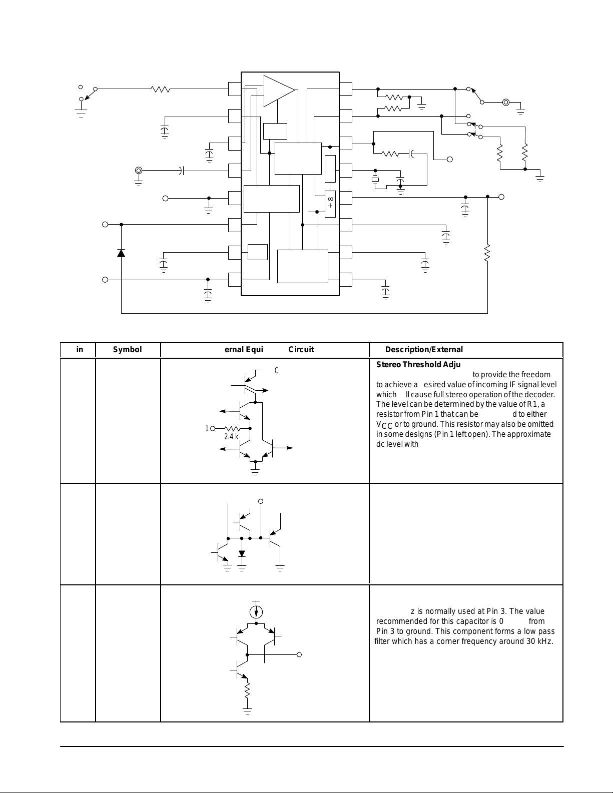
PIN FUNCTION DESCRIPTION
Internal Equivalent Circuit
V
CC
2.4 k
2
V
CC
2.0 k
Right
16
Left
15
10 k
R
O
R
O
R
L
Audio
Output
10 k
14
13
VCO
12
8
B
11
10
3.6 MHz
9
µ
10
47
µ
F
47
+
2.2 k
2.2 k
Loop
43 pF
V
+
47 µF
+
µ
F
0.22
0.47
+
F
+
µ
F
CC
2.2 k
Description/External Circuit Requirements
Stereo Threshold Adjustment Pin
The function of this circuit is to provide the freedom
ББББББББББББ
to achieve a desired value of incoming IF signal level
which will cause full stereo operation of the decoder.
ББББББББББББ
The level can be determined by the value of R1, a
ББББББББББББ
resistor from Pin 1 that can be connected to either
VCC or to ground. This resistor may also be omitted
ББББББББББББ
in some designs (Pin 1 left open). The approximate
ББББББББББББ
dc level with the pin left open is 0.6 Vdc.
ББББББББББББ
ББББББББББББ
AGC Filter Bypass Capacitor
An electrolytic capacitor is used as a bypass filter
ББББББББББББ
and it sets the time constant for the AGC circuit
ББББББББББББ
action. The recommended capacitor value is 10 µF
from Pin 2 to ground. The dc level at this pin varies
ББББББББББББ
as shown in the curve in Figure 13, AGC Voltage
versus Input Level.
ББББББББББББ
ББББББББББББ
ББББББББББББ
IF Amplifier Feedback Capacitor
ББББББББББББ
A capacitor which is specified to have a low ESR
at 450 kHz is normally used at Pin 3. The value
ББББББББББББ
recommended for this capacitor is 0.47 µF from
ББББББББББББ
Pin 3 to ground. This component forms a low pass
filter which has a corner frequency around 30 kHz.
ББББББББББББ
3
ББББББББББББ
ББББББББББББ
ББББББББББББ
ББББББББББББ
ББББББББББББ
3
Pin
Á
Á
Á
Á
Á
Á
Á
Á
Á
Á
Á
Á
Á
Á
Á
Á
Á
Á
Á
Á
Á
Á
Á
Á
Á
Á
Á
Á
Á
Á
Á
Á
Á
Á
Á
Á
Á
Á
Á
Á
Á
Á
Á
Á
Á
Á
Á
Á
Á
Á
Á
Á
Á
Á
Á
Á
Á
Á
Á
Á
Á
Á
Á
Á
Á
Á
Á
Á
Á
Á
Á
Á
Á
Á
Á
Á
Á
Á
Á
Á
Á
Á
Á
Á
Á
Á
Á
Á
Á
Á
Á
Á
Á
Á
Á
Á
Á
Á
Á
Á
Á
Á
Á
Á
Á
Á
Á
Á
4
ÁÁ
ÁÁ
ÁÁ
ÁÁ
ÁÁ
ÁÁ
5
ÁÁ
ÁÁ
ÁÁ
ÁÁ
Symbol
IF
in
ÁÁÁ
ÁÁÁ
ÁÁÁ
ÁÁÁ
ÁÁÁ
ÁÁÁ
Gnd
ÁÁÁ
ÁÁÁ
ÁÁÁ
ÁÁÁ
MC13028A
PIN FUNCTION DESCRIPTION
Internal Equivalent Circuit
БББББББББББББ
БББББББББББББ
БББББББББББББ
БББББББББББББ
БББББББББББББ
БББББББББББББ
БББББББББББББ
БББББББББББББ
БББББББББББББ
БББББББББББББ
4
5
Gnd
10 k
V
ref
Substrate
Circuit
Description/External Circuit Requirements
IF Amplifier Input
Pin 4 is the IF input pin. The typical input impedance
ББББББББББББ
at this pin is 10 k. The input should be ac coupled
ББББББББББББ
through a 0.01 µF capacitor.
ББББББББББББ
ББББББББББББ
ББББББББББББ
ББББББББББББ
Supply Ground
In the PCB layout, the ground pin should be
ББББББББББББ
connected to the chassis ground directly. This pin
ББББББББББББ
is the internal circuit ground and the silicon
substrate ground.
ББББББББББББ
ББББББББББББ
6
ÁÁ
ÁÁ
ÁÁ
ÁÁ
ÁÁ
ÁÁ
ÁÁ
7
ÁÁ
ÁÁ
ÁÁ
8
ÁÁ
ÁÁ
ÁÁ
ÁÁ
ÁÁ
ÁÁ
ÁÁ
ÁÁ
ÁÁ
ÁÁ
9
ÁÁ
ÁÁ
ÁÁ
ÁÁ
ÁÁ
ÁÁ
4
S
IND
ÁÁÁ
ÁÁÁ
ÁÁÁ
ÁÁÁ
ÁÁÁ
ÁÁÁ
ÁÁÁ
V
Ref
ÁÁÁ
ÁÁÁ
ÁÁÁ
CAP
Blend
ÁÁÁ
ÁÁÁ
ÁÁÁ
ÁÁÁ
ÁÁÁ
ÁÁÁ
ÁÁÁ
ÁÁÁ
ÁÁÁ
ÁÁÁ
I
Pilot
ÁÁÁ
ÁÁÁ
ÁÁÁ
ÁÁÁ
ÁÁÁ
ÁÁÁ
V
43 k
CC
30 k
Reference
Voltage
1.0 V
Blend Cap
Charging
Circuit
V
CC
Blend
Algorithm
Circuit
V
CC
9
Pilot Indicator
Driver Circuit
БББББББББББББ
БББББББББББББ
БББББББББББББ
БББББББББББББ
БББББББББББББ
БББББББББББББ
БББББББББББББ
БББББББББББББ
БББББББББББББ
БББББББББББББ
БББББББББББББ
БББББББББББББ
БББББББББББББ
БББББББББББББ
БББББББББББББ
БББББББББББББ
БББББББББББББ
БББББББББББББ
БББББББББББББ
БББББББББББББ
БББББББББББББ
БББББББББББББ
БББББББББББББ
БББББББББББББ
БББББББББББББ
БББББББББББББ
6
7
8
V
reg
Stereo Indicator Driver
This driver circuit is intended to light an LED or
ББББББББББББ
other indicator when the decoder receives the
ББББББББББББ
proper input signals and switches into the stereo
mode. The maximum amount of current that the
ББББББББББББ
circuit can sink is 10 mA.
ББББББББББББ
A current limiting resistor is applied externally to
ББББББББББББ
control LED brightness versus total power supply
current.
ББББББББББББ
ББББББББББББ
Regulated Voltage, 1.0 V
An electrolytic capacitor used as a bypass filter is
ББББББББББББ
recommended from Pin 7 to ground. The capacitor
value should be 10 µF.
ББББББББББББ
ББББББББББББ
Blend Capacitor
ББББББББББББ
The value of the capacitor on this pin will effect the
time constant of the decoder blend function. The
ББББББББББББ
recommended value is 10 µF from Pin 8 to ground.
ББББББББББББ
The dc level at Pin 8 is internally generated in
response to input signal level and signal quality. This
ББББББББББББ
pin is a key indicator of the operational state of the IC
ББББББББББББ
(see text Functional Description). It is recommended
to discharge the blend capacitor externally when
ББББББББББББ
changing stations.
ББББББББББББ
ББББББББББББ
ББББББББББББ
ББББББББББББ
Pilot I Detector Output
The Pilot I Detector output requires a 10 µF
ББББББББББББ
electrolytic capacitor to ground. The value of this
capacitor sets the pilot acquisition time. The dc
ББББББББББББ
level at Pin 9 is approximately 1.0 Vdc, unlocked,
ББББББББББББ
and 1.1 to 2.4 Vdc in the locked condition.
ББББББББББББ
ББББББББББББ
ББББББББББББ
MOTOROLA ANALOG IC DEVICE DATA
Pin
Á
Á
Á
Á
Á
Á
Á
Á
Á
Á
Á
Á
Á
Á
Á
Á
Á
Á
Á
Á
Á
Á
Á
Á
Á
Á
Á
Á
Á
Á
Á
Á
Á
Á
Á
Á
Á
Á
Á
Á
Á
Á
Á
Á
Á
Á
Á
Á
Á
Á
Á
Á
Á
Á
Á
Á
Á
Á
Á
Á
Á
Á
Á
Á
Á
Á
Á
Á
Á
Á
Á
Á
Á
Á
Á
Á
Á
Á
Á
Á
Á
Á
Á
Á
Á
Á
Á
Á
Á
Á
Á
Á
Á
10
ÁÁ
ÁÁ
ÁÁ
ÁÁ
ÁÁ
ÁÁ
ÁÁ
ÁÁ
11
ÁÁ
ÁÁ
ÁÁ
ÁÁ
ÁÁ
ÁÁ
ÁÁ
ÁÁ
ÁÁ
12
ÁÁ
ÁÁ
ÁÁ
ÁÁ
ÁÁ
Symbol
Q
Pilot
ÁÁÁ
ÁÁÁ
ÁÁÁ
ÁÁÁ
ÁÁÁ
ÁÁÁ
ÁÁÁ
ÁÁÁ
PILOT
fil
ÁÁÁ
ÁÁÁ
ÁÁÁ
ÁÁÁ
ÁÁÁ
ÁÁÁ
ÁÁÁ
ÁÁÁ
ÁÁÁ
V
CC
ÁÁÁ
ÁÁÁ
ÁÁÁ
ÁÁÁ
ÁÁÁ
MC13028A
PIN FUNCTION DESCRIPTION
Internal Equivalent Circuit
5.0 k
30 k
V
10
CC
V
V
CC
CC
2.0 k
V
CC
12
V
CC
БББББББББББББ
БББББББББББББ
БББББББББББББ
БББББББББББББ
БББББББББББББ
БББББББББББББ
БББББББББББББ
БББББББББББББ
БББББББББББББ
БББББББББББББ
БББББББББББББ
БББББББББББББ
11
БББББББББББББ
БББББББББББББ
БББББББББББББ
БББББББББББББ
БББББББББББББ
БББББББББББББ
БББББББББББББ
БББББББББББББ
БББББББББББББ
БББББББББББББ
Description/External Circuit Requirements
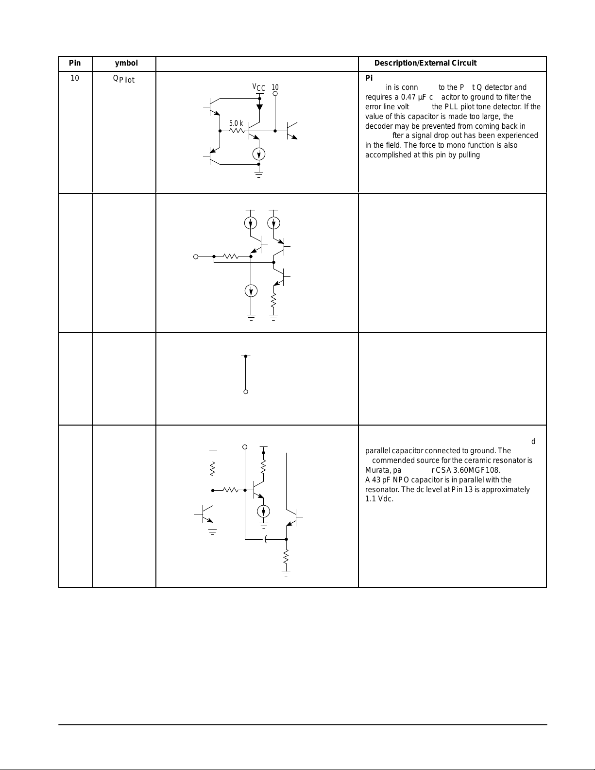
Pilot Q Detector Output
ББББББББББББ
This pin is connected to the Pilot Q detector and
requires a 0.47 µF capacitor to ground to filter the
ББББББББББББ
error line voltage at the PLL pilot tone detector. If the
ББББББББББББ
value of this capacitor is made too large, the
decoder may be prevented from coming back into
ББББББББББББ
stereo after a signal drop out has been experienced
in the field. The force to mono function is also
ББББББББББББ
accomplished at this pin by pulling the dc voltage
ББББББББББББ
level at the pin below 1.0 V.
ББББББББББББ
ББББББББББББ
Pilot Signal Input
ББББББББББББ
A capacitor to ground forms a filter for the pilot input
signal. The recommended value of the capacitor is
ББББББББББББ
0.22 µF . The dc level at Pin 1 1 is approximately
ББББББББББББ
1.0 Vdc.
ББББББББББББ
ББББББББББББ
ББББББББББББ
ББББББББББББ
ББББББББББББ
ББББББББББББ
Supply Voltage (VCC)
The operating supply voltage range is from 1.8 Vdc
ББББББББББББ
to 12 Vdc.
ББББББББББББ
ББББББББББББ
ББББББББББББ
ББББББББББББ
13
ÁÁ
ÁÁ
ÁÁ
ÁÁ
ÁÁ
ÁÁ
ÁÁ
ÁÁ
ÁÁ
ÁÁ
MOTOROLA ANALOG IC DEVICE DATA
OSC
in
ÁÁÁ
ÁÁÁ
ÁÁÁ
ÁÁÁ
ÁÁÁ
ÁÁÁ
ÁÁÁ
ÁÁÁ
ÁÁÁ
ÁÁÁ
БББББББББББББ
БББББББББББББ
БББББББББББББ
БББББББББББББ
БББББББББББББ
БББББББББББББ
БББББББББББББ
БББББББББББББ
БББББББББББББ
БББББББББББББ
2.2 k
V
13
V
reg
reg
3.1 k
3.0 k
6.3 pF
15 k
Oscillator Input
The oscillator pin requires a ceramic resonator and
ББББББББББББ
parallel capacitor connected to ground. The
ББББББББББББ
recommended source for the ceramic resonator is
Murata, part number CSA 3.60MGF108.
ББББББББББББ
A 43 pF NPO capacitor is in parallel with the
resonator. The dc level at Pin 13 is approximately
ББББББББББББ
1.1 Vdc.
ББББББББББББ
ББББББББББББ
ББББББББББББ
ББББББББББББ
ББББББББББББ
ББББББББББББ
5
Pin
Á
Á
Á
Á
Á
Á
Á
Á
Á
Á
Á
Á
Á
Á
Á
Á
Á
Á
Á
Á
Á
Á
Á
Á
Á
Á
Á
Á
Á
Á
Á
Á
Á
Á
Á
Á
Á
Á
Á
Á
Á
Á
Á
Á
Á
Á
Á
Á
Á
Á
Á
Á
Á
Á
Á
Á
Á
Á
Á
Á
Á
Á
Á
Á
Á
Á
Á
Á
Á
Á
Á
Á
Á
Á
Á
Á
Á
Á
Á
Á
Á
14
ÁÁ
ÁÁ
ÁÁ
ÁÁ
ÁÁ
ÁÁ
ÁÁ
ÁÁ
ÁÁ
ÁÁ
ÁÁ
Symbol
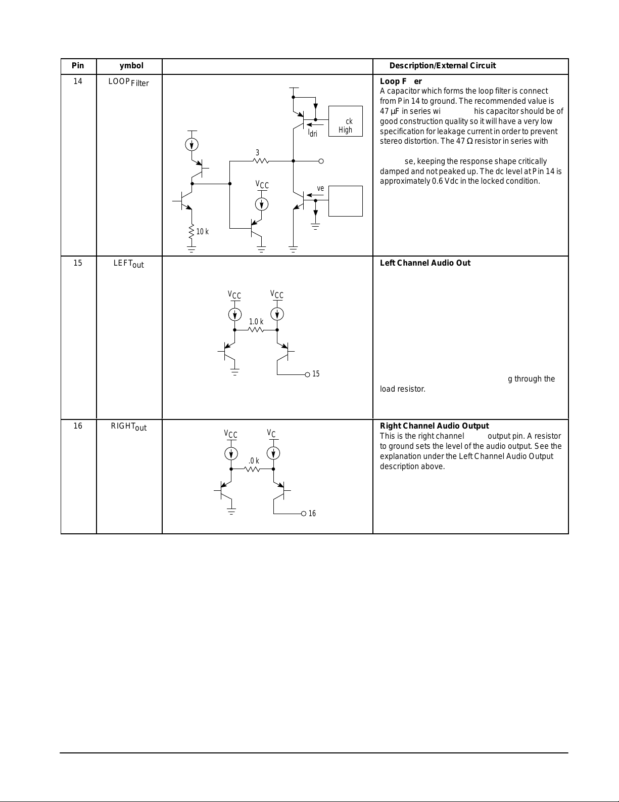
LOOP
Filter
ÁÁÁ
ÁÁÁ
ÁÁÁ
ÁÁÁ
ÁÁÁ
ÁÁÁ
ÁÁÁ
ÁÁÁ
ÁÁÁ
ÁÁÁ
ÁÁÁ
MC13028A
PIN FUNCTION DESCRIPTION
Internal Equivalent Circuit
V
БББББББББББББ
БББББББББББББ
БББББББББББББ
V
CC
БББББББББББББ
БББББББББББББ
БББББББББББББ
БББББББББББББ
БББББББББББББ
БББББББББББББ
БББББББББББББ
10 k
БББББББББББББ
390
V
CC
CC
I
drive
I
drive
Fast
Lock
High
14
Fast
Lock
Low
Description/External Circuit Requirements
Loop Filter
ББББББББББББ
A capacitor which forms the loop filter is connected
from Pin 14 to ground. The recommended value is
ББББББББББББ
47 µF in series with 47 Ω. This capacitor should be of
ББББББББББББ
good construction quality so it will have a very low
specification for leakage current in order to prevent
ББББББББББББ
stereo distortion. The 47 Ω resistor in series with the
capacitor controls the PLL corner frequency
ББББББББББББ
response, keeping the response shape critically
ББББББББББББ
damped and not peaked up. The dc level at Pin 14 is
approximately 0.6 Vdc in the locked condition.
ББББББББББББ
ББББББББББББ
ББББББББББББ
ББББББББББББ
ББББББББББББ
15
ÁÁ
ÁÁ
ÁÁ
ÁÁ
ÁÁ
ÁÁ
ÁÁ
ÁÁ
ÁÁ
ÁÁ
16
ÁÁ
ÁÁ
ÁÁ
ÁÁ
ÁÁ
ÁÁ
ÁÁ
LEFT
out
ÁÁÁ
ÁÁÁ
ÁÁÁ
ÁÁÁ
ÁÁÁ
ÁÁÁ
ÁÁÁ
ÁÁÁ
ÁÁÁ
ÁÁÁ
RIGHT
out
ÁÁÁ
ÁÁÁ
ÁÁÁ
ÁÁÁ
ÁÁÁ
ÁÁÁ
ÁÁÁ
БББББББББББББ
БББББББББББББ
БББББББББББББ
БББББББББББББ
БББББББББББББ
БББББББББББББ
БББББББББББББ
БББББББББББББ
БББББББББББББ
БББББББББББББ
БББББББББББББ
БББББББББББББ
БББББББББББББ
БББББББББББББ
БББББББББББББ
БББББББББББББ
БББББББББББББ
V
CC
V
CC
1.0 k
1.0 k
V
CC
15
V
CC
16
Left Channel Audio Output
This is the left channel audio output pin from which
ББББББББББББ
the IC can provide 1.3 µApp drive current for each
ББББББББББББ
percent of mono modulation. A resistor to ground
sets the level of the audio output.
ББББББББББББ
For example,
ББББББББББББ
drive per % mod) = 130 µApp flowing through the
ББББББББББББ
load resistor. (For a 2.2 k load, 286 mVpp is then
the output signal voltage.) When dealing with
ББББББББББББ
stereo signals, multiply the mod level by 2; i.e.
(left only mod) x 2 (stereo factor) x 1.3 µApp (IC
ББББББББББББ
drive per % mod) = 130 µApp flowing through the
ББББББББББББ
load resistor.
ББББББББББББ
ББББББББББББ
Right Channel Audio Output
ББББББББББББ
This is the right channel audio output pin. A resistor
to ground sets the level of the audio output. See the
ББББББББББББ
explanation under the Left Channel Audio Output
ББББББББББББ
description above.
ББББББББББББ
ББББББББББББ
ББББББББББББ
ББББББББББББ
100%
(mono mod) x 1.3 µApp (IC
50%
6
MOTOROLA ANALOG IC DEVICE DATA
 Loading...