

Motorola MC13027P, MC13027DW, MC13022DW, MC13022P Datasheet
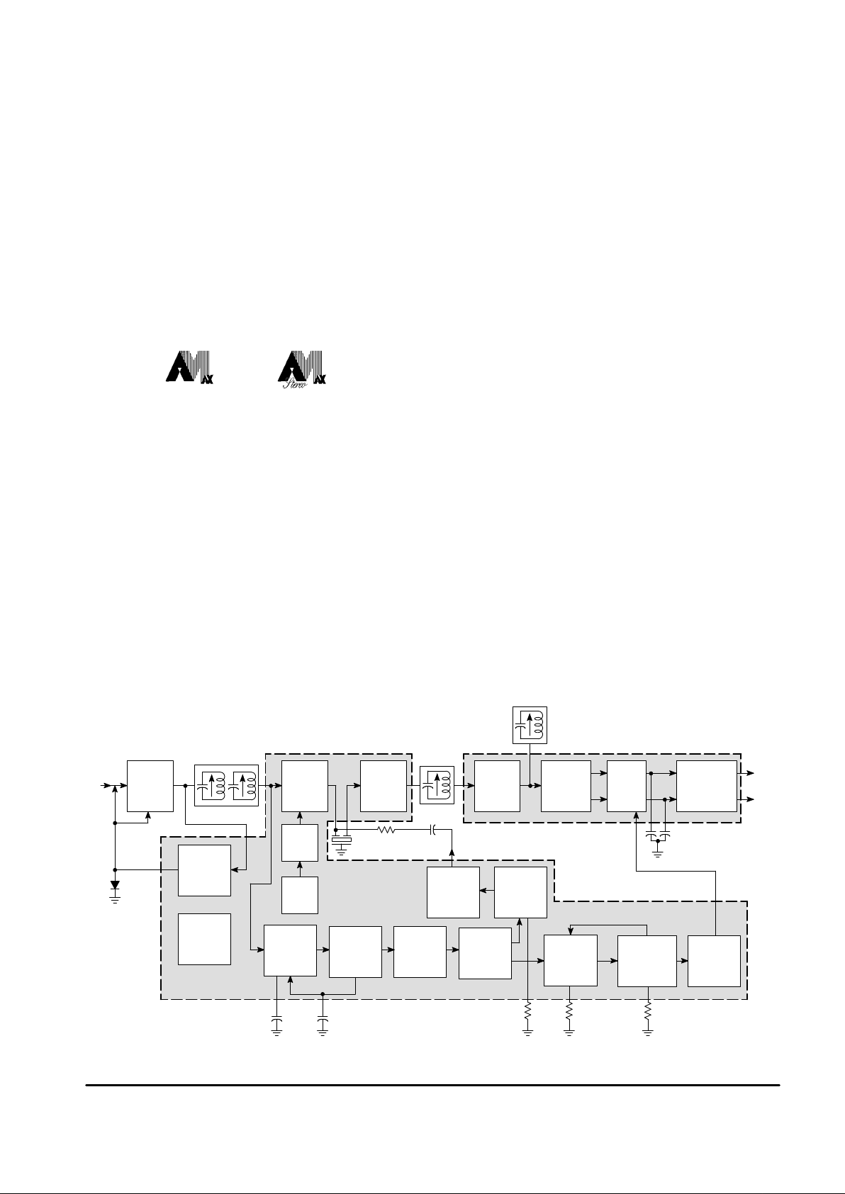
AMAX STEREO
IC CHIPSET
DW SUFFIX
PLASTIC PACKAGE
CASE 751D
(SO–20L)
20
1
Order this document from Analog Marketing
DW SUFFIX
PLASTIC PACKAGE
CASE 751F
(SO–28L)
28
1
20
1
28
1
MC13027
MC13122
P SUFFIX
PLASTIC PACKAGE
CASE 710
P SUFFIX
PLASTIC PACKAGE
CASE 738
1
MOTOROLA ANALOG IC DEVICE DATA
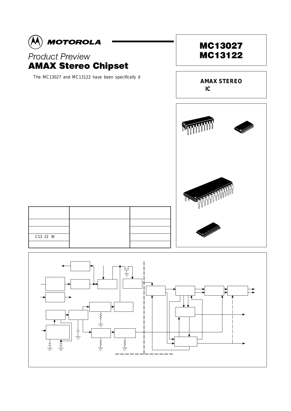
The MC13027 and MC13122 have been specifically designed for AM
radio which can meet the EIA/NAB AMAX requirements. They are
essentially the same as the MC13022A and MC13025 with the addition of
noise blanking circuitry. The noise blanker consists of a wide band amplifier
with an RF switch for blanking ahead the IF amplifier and a stereo audio
blanker with adjustable delay and blanking times.
• Operating Voltage Range of 6.0 V to 10 V
• RF Blanker with Built–In Wide Band AGC Amplifier
• Audio Noise Blanker with Audio Track and Hold
• Mixer Third Order Intercept of 8.0 dBm (115 dBµV)
• Wide Band AGC Detector for RF Amplifier
• Local Oscillator VCO Divide–by–4 for Better Phase Noise
• Buffered Local Oscillator Output at the Fundamental Frequency
• Fast Stereo Decoder Lock
• Soft Stereo Blend
• Signal Quality Detector to Control Variable Q–Notch Filters for Adaptive
Audio Bandwidth and Whistle Reduction
• Signal Quality Detector for AM Stereo
• Very Low Distortion Envelope and Synchronous Detectors
• Variable Bandwidth IF
ORDERING INFORMATION
Device
Operating
Temperature Range
Package
MC13027DW
SO–20L
MC13027P
–
°
°
Plastic DIP
MC13122DW
T
A
= –
40 ° to +85°C
SO–28L
MC13122P Plastic DIP
Fast
AGC
Control
Audio
Blanking
Functional Block Diagram
Oscillator
Buffer
Voltage
Controlled
Oscillator
Wide Band
AGC
AM
Detector
Automatic
Gain Controlled
RF Amplifier
Pulse
Detector
÷
4 Mixer
IF Amplifier
IF Amplifier
AGC
Shunt
Switch
Pulse Length
Timer
Pulse Delay
Timer
Signal Quality
Detector
Pilot
Detector
Decoder
Track & Hold
Post Detector
Filter
450 kHz IF
Signal Level
450 kHz Blend cos
θ
Fast Lock
Control
Stereo Indicator Lamp
Stop–Sense
RF AGC Meter Drive
Right Audio
Left Audio
Y es/NoI
RF
Blanking
AGC
Output
To Synthesizer
Osc
Tank
AGC
Input
RF
Input
RF Input
L
R
Q
Fast/
Slow
MC13027 MC13122
This device contains 428 active transistors. This device contains 670 active transistors.
Pulse Length
Timer
This document contains information on a product under development. Motorola reserves the
right to change or discontinue this product without notice.
Motorola, Inc. 1996 Issue 1
MC13027 MC13122
2
MOTOROLA ANALOG IC DEVICE DATA
MC13027
MAXIMUM RATINGS
Rating Symbol Value Unit
Power Supply Input Voltage V
CC
12 Vdc
Ambient Operating Temperature T
A
–40 to +85 °C
Storage Temperature Range T
stg
–60 to +150 °C
Operating Junction Temperature T
J
150 °C
NOTE: ESD data available upon request.
MC13027
ELECTRICAL CHARACTERISTICS (T
A
= 25°C, 8.0 VCC Test Circuit as shown in Figure 1.)
Characteristic
Min Typ Max Unit
Supply Voltage Range (Pin 8) – 6.0 to 10 – V
Wideband (WB) AGC Threshold – 1.0 – mVrms
IF Output DC Current – 1.0 – mAdc
Mixer DC Current Output – 0.83 – mAdc
Local Oscillator Output – 600 – mVpp
Wideband AGC Pull–Down Current (Pin 20) – 1.0 – mAdc
Power Supply Current – 16 – mAdc
Mixer 3rd Order Intercept Point (Pin 6) – 8.0 – dBm
Mixer Conversion Gain – 2.9 – mS
IF Amplifier Input Impedance (Pin 14) – 2.2 – kΩ
IF Amplifier Transconductance – 2.8 – mS
IF Amplifier Load Resistance (Pin 16) – 5.7 – kΩ
IF Amplifier Collector Current (Pin 16) – 990 – µA
MC13027 MC13122
3
MOTOROLA ANALOG IC DEVICE DATA
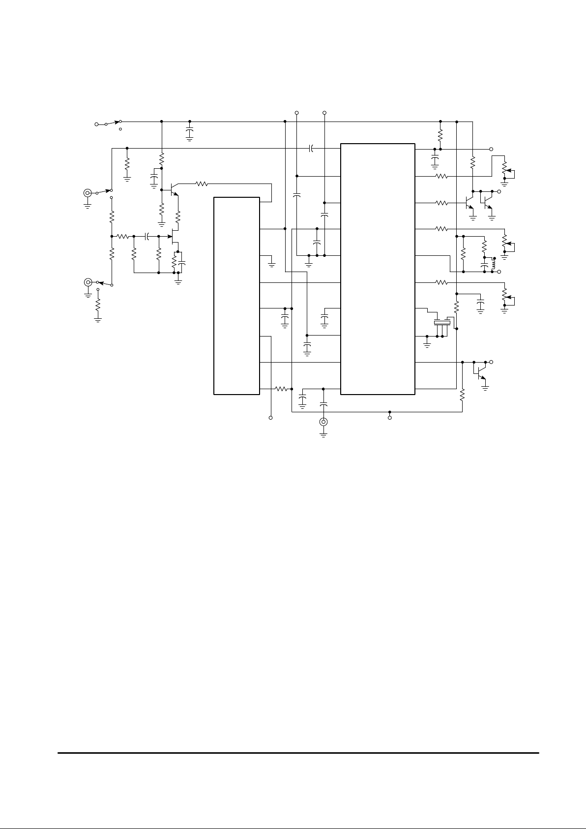
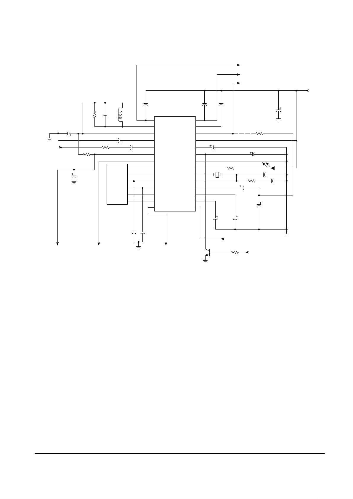
Figure 1. MC13027 Test Circuit
34
RF In
1
2
3
4
5
6
7
8
V
CC
Gnd
Mixer In
Mixer 4.0 V
Tuning V
VCLO
VCLO 4.0 V
C87
0.1
R2
82
R1
100 k
RL2
51
RM2
16.7
R299
51
RM1
16.7
Pulse In
RF In
Pulse On
RF
Mixer In
Blanker In
WB AGC
RL1
51
R10
56 k
C5
22
µ
F
C14
47
µ
F
R200
560 k
V
CC
V
CC
On
R4
47
R11
47
Q1
MMBFJ309L
RM5
16.7
CM1
0.01
C11
0.1
C293
10
µ
F
C6
0.1
R201
120
C37
0.01
100
LO Out
Tuning Voltage 4.0 V Reg
C9
47
µ
F
C16
10
µ
F
C26
1.0
µ
F
C10
0.01
R20
47 k
C90
0.1
R3b
10 k
R18
2.35 k
R1b
10 k
R16
3.3 k
RT1
39 k
Q2
(Note 1)
Q3
(Note 1)
R19
500 k
R17
500 k
R15
500 k
C103
0.1
R12
1.8 k
Q1b
(Note 1)
R5b
390 k
R21
510
C16 120
L2 1.0 mH
Murata
SFG450E
20
19
18
17
16
15
14
13
12
11
1
2
3
4
5
6
7
8
9
10
WB AGC
Out
Audio
Blank Time
Audio
Blank Pulse
Audio Blank
Delay Time
IF Out
RF Blank
Time
IF In
Gnd2
RF Blank
Mixer Out
WB AGC
In
Blanker
AGC
Feedback
4.0 V Reg
RF Gnd
Mixer In
Blanker RF In
4.0 Filter
V
CC
VCO
LO Out
WB AGC Out
Audio Blank
IF Out
RF Blank
R2b
10 k
12
5
V
CC
AGC Feedback
MC13027
RF Module
Q4
MMBT3904L
V
CC
V
CC
+
+
+
+
+
+
NOTE: 1.General purpose NPN transistor 2N3904 or equivalent.
MC13027 MC13122
4
MOTOROLA ANALOG IC DEVICE DATA
MC13122
MAXIMUM RATINGS
Rating Symbol Value Unit
Power Supply Input Voltage V
CC
12 Vdc
Stereo (Pilot) Indicator Lamp Current (Pin 21) – 30 mAdc
Operating Ambient Temperature T
A
–40 to +85 °C
Storage Temperature Range T
stg
–65 to +150 °C
Operating Junction Temperature T
J(max)
150 °C
Power Dissipation Derated above 25°C P
D
1.25 Ω
p
D
10 mW/C
NOTE: ESD data available upon request.
MC13122
ELECTRICAL CHARACTERISTICS
(VCC = 8.0 V , TA = 25°C, Test Circuit of Figure 2.)
Characteristic
Min Typ Max Unit
Power Supply Operating Range 6.0 8.0 10 V
Supply Current Drain (Pin 25) 10 20 25 mA
Minimum Input Signal Level, Unmodulated, for AGC Start – 5.0 – mV
Audio Output Level, 50% Modulation, L Only or R Only 290 400 530 mV rms
Audio Output Level, 50% Mono 140 200 265 mV rms
Output THD, 50% Modulation (Monaural Stereo) – 0.3 0.8 %
p, ( )
– 0.5 1.6
Channel Separation, L Only or R Only, 50% Modulation 22 35 – dB
IF Input Voltage Range – 1.0–1000 – mV
IF Input Resistance Range – 10 to 50 –
kΩ
IF Amplifier Transconductance – 9.6 – mS
IF Detector Circuit Impedance – 8.3 – kΩ
Input AGC Threshold – 5.0 – mV
Stop–Sense Output Range – 2.2 to 4.0 – V
Audio Output Impedance at 1.0 kHz (Pins 7 and 14) – 300 – Ω
Stereo Indicator Lamp Leakage – – 1.0 µA
Stereo Indicator Saturation Voltage @ 3.0 mA – – 200 mVdc
Oscillator Capture Range – ±3.0 – kHz
MC13027 MC13122
5
MOTOROLA ANALOG IC DEVICE DATA
Figure 2. MC13122 Test Circuit
MC13122
IC2
U2
THB122
1
Ch2 Out
2
3
4
5
6
Ch2 Cont
Ch2 In
Ch1 In
Ch1 Cont
Ch1 Out
23
I Det
24
25
26
27
28
L–R Det
Q Det
V
CC
Loop Filt
Blend
17
Gnd
18
19
20
21
22
Pilot Ind
Osc Out
Osc In
Pilot Det I
Pilot I
16
Pilot Q
15
Audio Blank
E Det
Det In
3.0 V Reg
AGC
IF In
SS
L Out
L Filt In
L Filt Ctr
L Mat Out
R Mat Out
R Filt Ctr
R Filt In
R Out
6
5
4
3
2
1
12
11
10
9
8
7
13
14
R10
13 k
C3 47
µ
F
C4 10 µF
450 kHz IF In
SS Out Left
Audio Out
Right
Audio Out
C6
1.0
µ
F
C1
1000
.01
100 k
R6
10 k
R5
C28
1000
C27
1000
10001000
33 k
R11
C16
0.47
µ
F
C17
10 µF
C31
1.0
µ
F
1000 C30
3.9 k
R12
C18
22
µ
F
1.0 k
R20
X1
3.6 MHz
AF Blank
Blend Disable
8.0 V
Envelope Det Out
I Detector Out
Q Detector Out
2.2 k
R26
C23 22
µ
F
C24 47
µ
F
C22
220
µ
F
Stereo
D1
CA
MPS6515
Q3
C
B
E
51 C29
L1
1.0 mH
C2
120
MC13027 MC13122
6
MOTOROLA ANALOG IC DEVICE DATA
AMAX STEREO CHIPSET
What is AMAX?
In 1993, a joint proposal by the EIA (Electronic Industries
Association) and the NAB (National Association of
Broadcasters) was issued. It included a unified standard for
pre–emphasis and distortion for broadcasters as well as a set
of criteria for the certification of receivers. The purpose of this
proposal was to restore quality and uniformity to the AM band
and to make it possible for the consumer to receive high
quality signals using the AM band. The FCC has been
supportive of this initiative and has required all new
broadcast licensees to meet AMAX standards. The NAB and
EIA have continued to encourage receiver manufacturers by
offering the AMAX certification logo to be displayed on all
qualifying radios. This logo is shown below.
or
The Receiver Criteria
An AMAX receiver must have wide bandwidth: 7.5kHz for
home and auto, 6.5 kHz for portables. It must have some
form of bandwidth control, either manual or automatic,
including at least two bandwidth provisions, such as “narrow”
and “wide”. It must meet NRSC receiver standards for
distortion and deemphasis. It must have provisions for an
external antenna. It must be capable of tuning the expanded
AM band (up to 1700 kHz). And finally, home and auto
receivers must have effective noise blanking. All of these
requirements, except the noise blanking, have been met by
Motorola’s previous AM radio products, such as MC13025
Front End and the MC13022A C–QUAM stereo decoder. It is
the Noise Blanker requirement which is met by the two
devices on this data sheet, the MC13027 and MC13122.
Noise blanking, especially in AM auto radios, has become
extremely important. The combination of higher energy
ignitions, using multiple spark coils, along with increased use
of plastic in the auto body, have increased the noise energy
at the radio. Also, the consumer has learned to expect higher
quality audio due to advances in many other media. For the
AM band to sustain interest to the consumer, a truly effective
noise blanker is required.
The block diagram below shows the Motorola AMAX
stereo chipset. It offers a two–pronged approach to noise
blanking which is believed to be the most effective yet offered
in the consumer market. The initial blanking takes place in
the output of the mixer, using a shunt circuit triggered by a
carefully defined wideband receiver. For most noises, some
residual audible disturbance is almost always still present
after this process. The disturbance becomes stretched and
delayed as it passes through the rest of the selectivity in the
receiver. The stretching and delay are predictable, so the
MC13027 can provide a noise blanking pulse with the correct
delay and stretch to the output stages of the MC13122
decoder. The MC13122 has a Track and Hold circuit which
receives the blanking signal from the Front End and uses it to
gently hold the audio wherever it is as the pulse arrives, and
hold that value until the noise has passed. The combined
effect is dramatic. A wide range of types of noise is
successfully suppressed and the resulting audio seems
almost clean until the noise is so intense that the blanking
approaches full–time.
The amount of extra circuitry to accomplish noise blanking
is relatively small. The external components for this added
capability are shown in Figure 3. In the MC13027 Front end,
the noise receiver/detector requires two capacitors. The
presettings for blanking timing and blanking delay require
three external fixed resistors. Finally the decoder requires
two track and hold capacitors to store the “audio” voltage
during the track and hold function.
Figure 3. AMAX Stereo Receiver with Noise Blanker
MC13027 MC13122
Audio Blank
450 kHz
Filter
RF Attenuate
Left
Right
RF In
Pin
Diode
Reset
AGC
RF
Amplifier
Mixer
IF
Amplifier
AGC’d IF
Amplifier
AM
Stereo
Decoder
Track
and
Hold
Variable
Notch Filter
Wideband
AGC
4.0 V
Regulator
Divide
by 4
VCO
RF
Attenuator
Switch
RF Blank
Timer
AGC’d RF
AmplifierAMDetector
Audio
Reject
Filter
Pulse
Detector
Delay
Timer
Audio Blank
Timer
Audio
Blank
Switch
MC13027 MC13122
7
MOTOROLA ANALOG IC DEVICE DATA
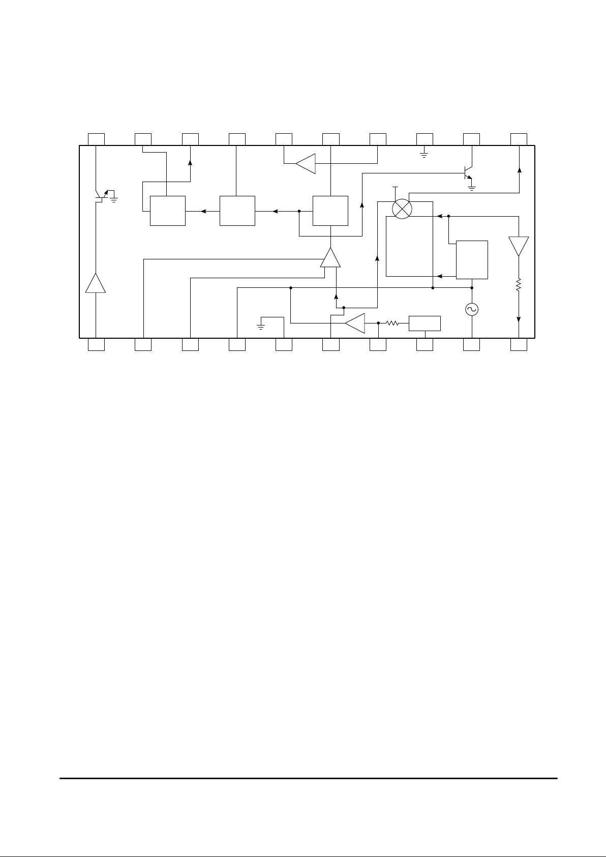
Figure 4. MC13027 Internal Block Diagram
20 19 18 17 16 15 14 13 12 11
12345678910
WB AGC Amp
Mixer
IF Amp
NB Amp
V
CC
÷
4
RF Time
MV
AF Del
MV
AF Time
MV
X1
Reg
X1
WB AGCInBlanker
AGC
Feedback 4.0 V Reg RF Gnd Mixer In
Blanker RF In
4.0 Filter V
CC
VCO LO Out
WB AGC
Out
Audio
Blank Time
Audio
Blank Pulse
Audio Blank
Delay Time
IF Out
RF Blank
Time
IF In Gnd2 RF Blank Mixer Out
MC13027 FUNCTIONAL DESCRIPTION
The MC13027 contains the mixer, wide band AGC
system, local oscillator, IF pre–amplifier and noise blanker for
an AM radio receiver. It is designed to be used with the
MC13122 to produce a complete AM stereo receiver. The
VCO runs at 4 (Fin+FIF) and is divided internally by 4 for the
mixer input and local oscillator buffered output. Dividing the
VCO reduces the phase noise for AM stereo applications.
The noise blanker input is connected in parallel with the
mixer input at Pin 6. The noise blanker circuitry contains a
high gain amplifier with its own AGC so it remains linear
throughout the mixer’s linear range. It can detect noise
pulses as low as 120 µV and generates three pulses when
the noise threshold is exceeded. The width and timing of the
blanking pulses is set by the resistors connected to Pins 15,
17 and 19. The resistor on Pin 15 sets the length of the RF
blanking pulse and determines the time the transistor on
Pin 12 is “on”. The audio blanking pulse delay is set by the
resistor on Pin 17 and the width by the resistor on Pin 19.
This is necessary because the IF filtering delays and
stretches the noise as it arrives at the detector. The transistor
on Pin 18 goes “on” to cause noise blanking in the track and
hold circuit in the MC13122 (Pin 15).
Wideband AGC is used in auto receivers to prevent
overload – it drives the base of a cascode transistor RF
amplifier and also a pin diode at the antenna (See Figures 6
and 7).
A low gain IF amplifier between Pins 14 and 16 is used as
a buffer amplifier between the mixer output filter and IF filter.
The input resistance of the IF amplifier is designed to match
a ceramic IF filter. The gain of the IF amplifier is determined
by the impedance of the load on Pin 16.
MC13027 MC13122
8
MOTOROLA ANALOG IC DEVICE DATA
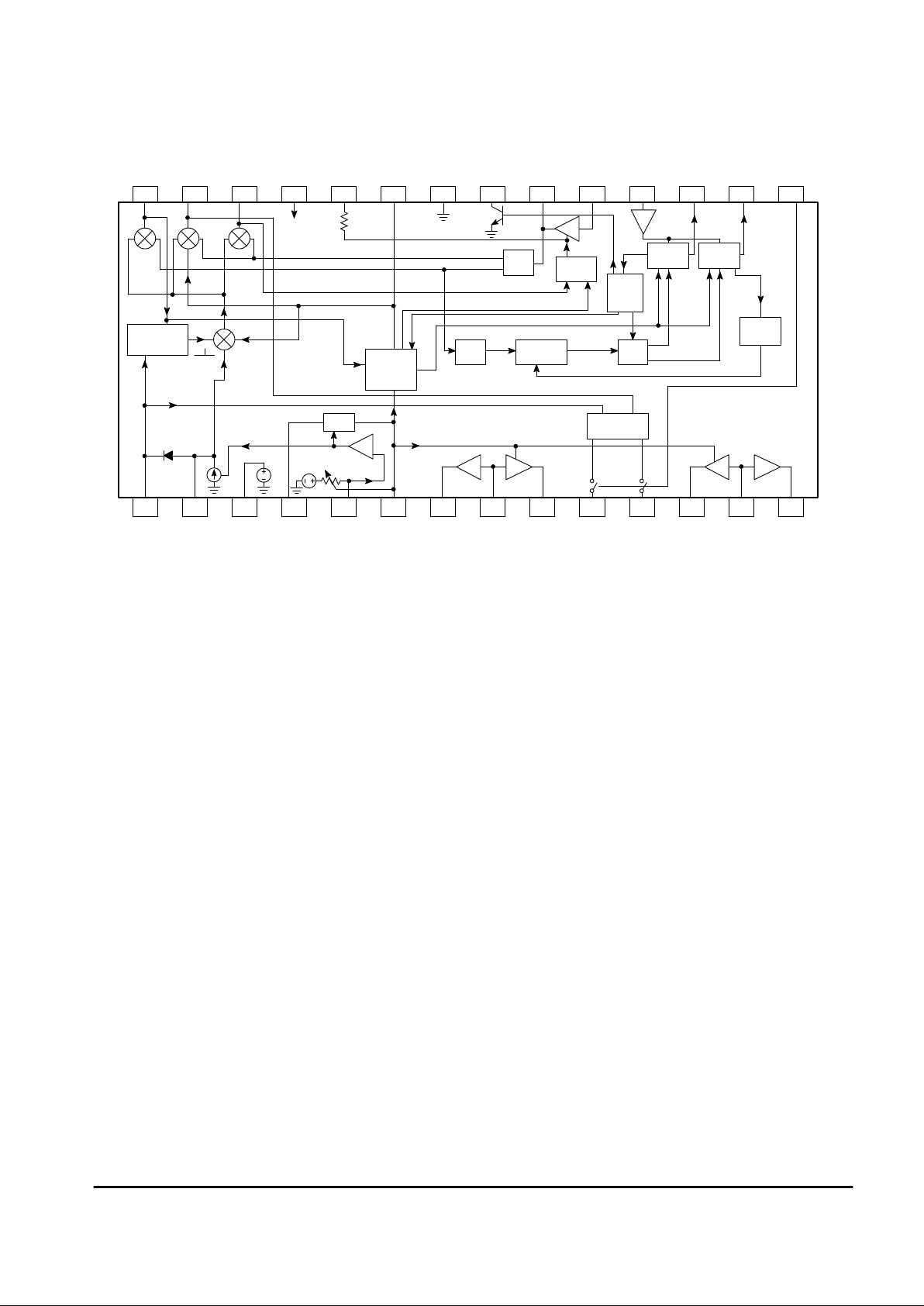
Figure 5. MC13122 Internal Block Diagram
28 27 26 25 24 23 22
1234567
21 20 19 18
891011
17 16 15
12 13 14
I L–R Q
V
CC
VGA
±
0.9
VGA
±
0.9
LR
LevelFast AGC
1.0 V
3.0 V
AGC
Matrix
C–QUAM
Comparator
Blend
Disable
450 <90
°
450 <0
°
Signal
Quality
Detector
÷
32
÷
137/144
÷
4
Count
Control
Clamp
25.6 Hz 24.4 Hz
Fast Lock
VCO
Loop
Driver
Pilot
Level
Det
÷
8
Pilot I
Det
Pilot Q
Det
cos
θ
330
Loop
Filt
Blend Gnd Pilot Ind Osc Out Osc In Pilot Det I Pilot I Pilot Q
Audio
Blank
L–R
L+R
IF Amp
V
CC
Q DetL–R DetI Det
IF In SS L Out L Filt In L Filt Ctr L Mat
Out
R Mat
Out
R Filt
Ctr
R Filt In R OutAGC3.0 V
Reg
Det InE Det
MC13122 FUNCTIONAL DESCRIPTION
The MC13122 is designed to accept a 450 kHz C–QUAM
input signal from approximately 1.0 mV to 1.0 V and produce
L and R audio output signals. It has additional features: stop
signal, variable bandwidth IF and audio response, stereo
indicator driver and track and hold noise blanking.
The IF amplifier on Pin 5 has its own AGC system. It
operates by varying the input resistance on Pin 5. With weak
signals below approximate 5.0 mV, the input resistance is
very high and the amplifier is at maximum gain. For this AGC
to be effective, it is necessary to feed the IF input signal from
a relatively high impedance. The input resistance variation
also reduces the Q of the coil (T1 in the application) so the
receiver bandwidth is narrow for weak signals and wide for
strong signals. The value of the input resistor (R5) is selected
for the desired loading of the IF coil. The impedance of the IF
coil on Pin 2 determines the IF gain. Pin 2 is also the input to
the C–QUAM decoder.
The IF signal drives the envelope (E), in–phase (I),
quadrature (Q) and (L–R) detectors. The E detector is a
quasi–synchronous true envelope detector. The others are
true synchronous detectors. The E detector output provides
the L+R portion of the C–QUAM signal directly to the matrix.
The AGC signal of the IF amplifier drives the signal strength
output at Pin 6. An external resistor on Pin 6 (sets the gain of
the AGC). The Pin 6 voltage is used to control the Q of the
audio notch filter, causing the audio bandwidth and depth of
the 10 kHz notch to change with signal strength. It is also
used as one of the inputs to the signal quality detector which
generates the stop–sense and blend signal on Pins 6 and 23
respectively and tells the signal quality detector that the RF
input is below the AGC threshold.
VCO
The 3.6 MHz ceramic resonator on Pins 19 and 20 is part
of a phase locked loop which locks to the 450 kHz IF signal.
The 3.6 MHz is divided by 8 to produce in–phase and
quadrature signals for the I, Q and L–R detectors. It is also
divided by 32, and 137/144 to provide signals for the pilot I
and Q detectors. The pilot detector is a unique circuit which
does not need filtering to detect the 25 Hz pilot.
Blend Circuit
The purpose of the blend circuit is to provide an AM stereo
radio with the capability of very fast lock times, protection
against stereo falsing when there is no pilot present and
control of the L–R signal so as to provide as much stereo
information as possible, while still sounding good in the
presence of noise or interference. The circuit also provides
an optional stop–sense usable by a radio with seek and/or
scan. The stop–sense signal provides a “stop” signal only
when the radio is locked on station, signal strength is above
minimum level, and the level of interference is less than a
predetermined amount. The last feature prevents stopping
on frequencies where there is is a multiplicity of strong
co–channel stations. It is common for AM radios without this
capability to stop on many frequencies with unlistenable
stations, especially at night.
The blend circuit controls the PLL fast lock, pilot detector,
IF amplifier AGC rate, decoder L–R gain, cosθ compensation
and stop–sense as a function of the voltage on a signal
external blend capacitor. Timing is determined by the rate of
change of voltage on the blend cap. Timing is changed by
varying charge and discharge current and pulled down by a
current source, switch, and optionally an external switch. The
current sources and switches are controlled by various
measures of signal quality, signal strength, and presence or
absence of pilot tone.

MC13027 MC13122
9
MOTOROLA ANALOG IC DEVICE DATA
Detectors
In AM stereo operation, the Q detector delivers pilot signal
via an external low–pass filter to the pilot detector input (Pin
18). The E and I detectors drive the C–QUAM comparator.
The L–R signal and the output of the envelope detector are
combined in the matrix to produce the L and R signals. The
C–QUAM system modifies the in–phase and quadrature
components of the transmitted signal by the cosine of the
phase angle of the resultant carrier, for proper stereo
decoding. An uncompensated L–R would be distorted,
primarily by second harmonics. Where there is noise or
interference in the L–R, it has been subjectively determined
that reducing the cosθ compensation at the expense of
increased distortion sounds better than full decoding. The
blend line operates over a small voltage range to eliminate
cosine compensation.
Signal Quality Detector – Blend Voltage Control
The signal quality detector output is dependent on signal
strength, over–modulation, and whether or not the blend pin
has been pulled low prior to searching. Over–modulation
usually occurs when a radio is tuned one channel away from
a desired strong signal, so this prevents stopping one
channel away from a strong signal.
In a radio tuned to a strong, interference free C–QUAM
station, the blend voltage will be approximately 3.6 V. In the
presence of noise or interference, when the modulation
envelope is at a minimum, it is possible for the I detector to
produce a negative, or below zero carrier signal. The Signal
Quality Detector produces an output each time the negative
I exceeds 4%. The output of the detector sets a latch. The
output of the latch turns on current source which pulls down
the voltage of the blend cap at a predetermined rate. The
latch is then reset by a low frequency signal from the pilot
detector logic. This produces about a 200 mV change each
time 4% negative I is detected. Tables 1 and 2 describe the
blend behavior under various conditions.
When the blend voltage reaches 2.2 V a blend control
circuit starts to reduce the amplitude of the L–R signal fed to
the decoder matrix. By 1.5 V the L–R has been reduced by
about 40 dB. At lower voltages it is entirely off and the
decoder output is monaural. This reduction of L–R signal, or
blend as it is commonly called when done in FM stereo
radios, reduces undesirable interference effects as a function
of the amount of interference present.
Stop–Sense
Stop–sense is enabled when the blend voltage is
externally pulled below 0.45 V. An input from the AGC
indicating minimum signal, or detection of 10% negative I will
cause the stop–sense pin to be pulled low. With signals
greater than the AGC corner and less than 10% interference
the stop–sense will be a minimum of 1.0 V below the 3.0 V
line. Very rapid scanning is possible because the radio can
scan to the next frequency as soon as the stop–sense goes
low. The maximum wait time, set by the radio, is only reached
on good stations.
The decoder will not lock on an adjacent channel because
it is out of the lock range of the PLL. The beat note produced
in the I detector by the out of lock condition will trigger the
10% negative I detector.
Sequence For Seek Scan
• Change Station – Pull–Down Blend
• Wait Approximately 50 ms for Synthesizer and Decoder
PLL to Lock
• Observe Pin 6 Voltage
• If it is Above 2.0 V and Stays Above 2.0 V for
Approximately 800 ms, Stay on the Station
• No IF Count Now Needed
• No AGC Level Detector Needed
Table 1. Normal Sequence When Changing Stations
External Pull–Down of
Blend Capacitor to Under
0.47 V
– Increased Current Supplied to
Loop Driver for Fast Lock
– Fast AGC Activated
– Extra Current Pull–Up Activated
on Blend Capacitor
– Pilot Detector Disabled
– Loop Locks
– Stop–Sense Activated
Blend Released – Blend Capacitor Pulled Up to
0.7 V – Stops
– Fast Lock Current Removed
– Fast AGC Turned Off
– Pilot Detector Enabled
Pilot Detected – Stereo Indicator Pin Pulled Low
– Blend Voltage Pulled Positive
Rapidly
Blend Voltage Reaches
1.4 V
– Audio Starts Into Stereo
– 10% Negative I Detector
Enabled
Blend Voltage Reaches
2.2 V
– Stereo Separator Reaches 20
to 25 dB
– Rapid Current Pull–Up Turned
Off
– 4% Negative I Detector Enabled
Blend Voltage Reaches
3.0 V
– cosθ Enabled – Full C–QUAM
Decoding
– Blend Voltage Continues to Rise
to 3.6 V and Stops
Table 2. Operation In Adverse Conditions
4% Negative I Detected – Blend Pulls Down
Approximately 200 mV for Each
Event – Acts Like One–Shot
– Stops at 2.2 V – cosθ Has Been
Defeated, Almost Full Stereo
Remains
10% Negative I Detected – Blend Pulls Down 200 mV for
Each Event
– Stops at 1.4 V – Stereo Has
Blended to Mono
– Resets Fast Pull–Up if Blend
Has Not Been Above 2.2 V
50% Negative I Detected
(Out of Lock)
– Blend Pulls Down Fast During
Event
– Stops at 0.47 V
– Resets Fast Pull–Up
– Pilot Indicator Turned Off
Minimum Signal Level
Detected
– Resets Fast Pull–Up
– Pulls Down to 0.7 V
 Loading...