

Motorola MC13017P Datasheet
Device
Operating
Temperature Range
Package
SEMICONDUCTOR
TECHNICAL DATA
NTSC/PAL CHROMA 10
COLOR TV and
TIMEBASE PROCESSOR
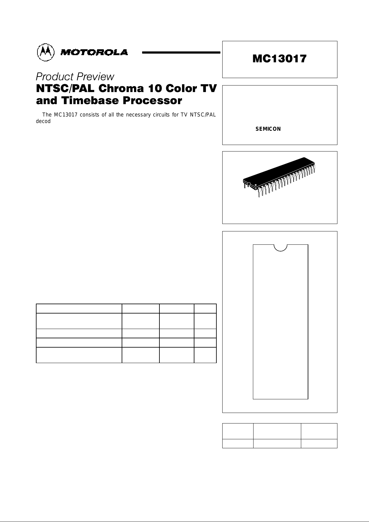
ORDERING INFORMATION
MC13017P TA = 0° to +70°C Plastic DIP
PIN CONNECTIONS
Order this document by MC13017/D
P SUFFIX
PLASTIC PACKAGE
CASE 711
40
1
20
19
212290° FLT
VCO FLT
U I/P
V I/P
18
17
16
15
14
23
24
25
26
27
Xtal Drive
Xtal FB
Gnd
DC Ref & BL
B O/P
ID
Sat
DL C
DL E
ACC
G O/P
R O/P
Sandcastle
Pulse
Brightness
Contrast
X–Ray
H. Freq
PD1
H. Flyback
PD2
H. O/P
H. Gnd
V
CC2
28
29
30
31
32
33
34
35
36
37
38
39
40
13
12
11
10
9
8
7
6
5
4
3
2
1
Chroma I/P
Hue
V
CC1
+ 12 V
Luma I/P
Sync I/P
Sync Sep Cap
V. Height
Ramp Cap
Buffer Ramp
V. Out
V. Feedback
V. Gnd
V
CC3
(Top View)
1
MOTOROLA ANALOG IC DEVICE DATA
The MC13017 consists of all the necessary circuits for TV NTSC/PAL
decoding and timebase processing. It forms a kit set with the MC44301 VIF
and the TDA3190 Sound IF and Power for a low cost, high performance CTV
system.
• On–Chip Sync Separator
• Dual Loop Horizontal Timebase
• Direct Locked Vertical Counter
• X–Ray Protection
• Noise Blanking on Sync Separator
• NTSC/PAL Color Decoding
• Direct Interface with SECAM TDA3030B
• 4.43/3.579 MHz Crystal Reference
• Three DC High Impedance Control Outputs for Contrast, Brightness, and
Saturation
• 12 V Supply
• Vertical Ramp Buffer Output
• Sandcastle Output
• Hue Control
MAXIMUM RATINGS
(TA = 25°C, unless otherwise noted.)
Rating
Symbol Value Unit
Power Supply Voltages V
CC1
, V
CC3
V
CC2
15
10
V
Operating Temperature Range T
A
0 to +70 5C
Storage Temperature Range T
stg
– 55 to +125 °C
Horizontal Output Voltage
Vertical Output Voltage
V
OH
V
OV
8.0
4.0
V
Motorola, Inc. 1995This document contains information on a product under development. Motorola reserves the right
to change or discontinue this product without notice.
MC13017
2
MOTOROLA ANALOG IC DEVICE DATA
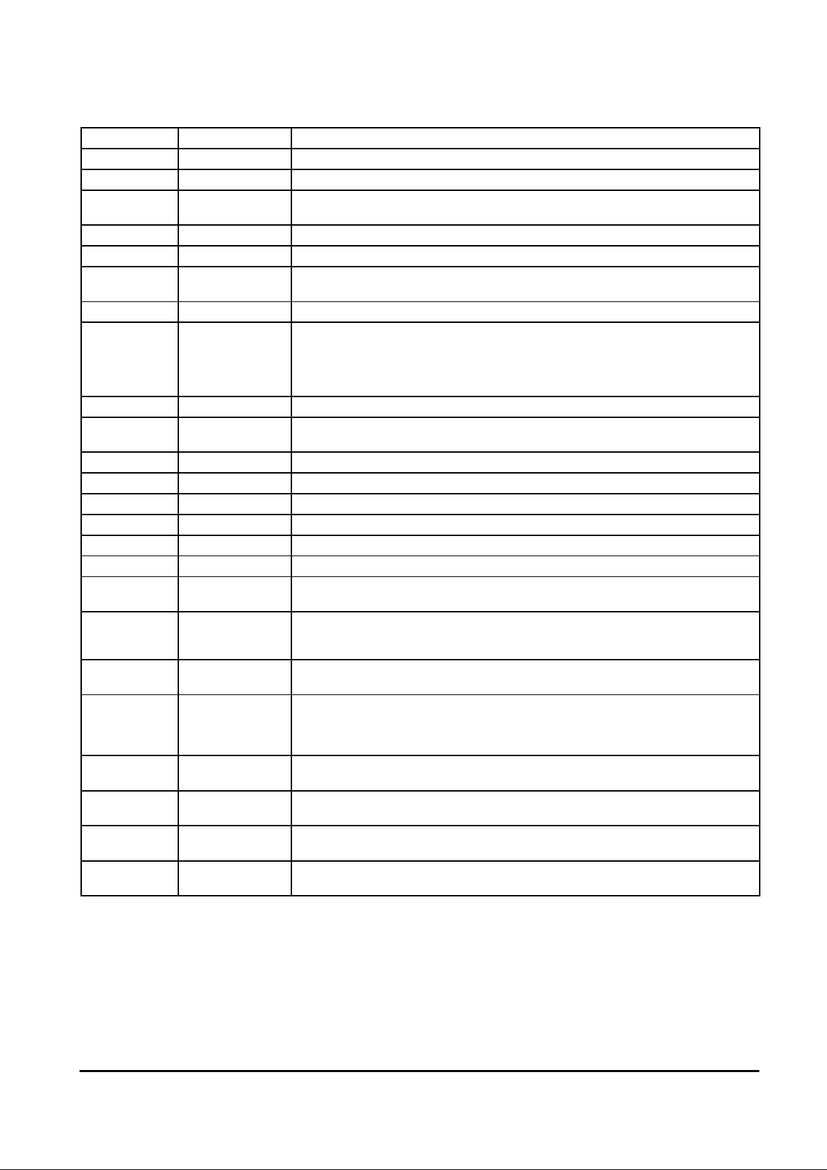
PIN FUNCTION DESCRIPTION
Pin Function Description
1 V
CC3
+12 V supply for V
CC2
power regulator.
2 Vert Gnd Vertical output analog ground.
3 Vert Feedback The Ramp on Pin 6 is internally inverted, level shifted and subtracted from the input to Pin 3. The
result appears as an output on an open collector at Pin 4.
4 Vert Out Vertical ramp output to external vertical power drive.
5 Buffer Ramp The vertical buffer ramp output of Pin 6.
6 Ramp Cap The external cap is charged by a current controlled through vertical height control Pin 7 to
produce a vertical ramp. The discharge of the cap is controlled internally by the vertical counter.
7 Vert Height Current input for vertical height control.
8, 9 Sync Sep Cap,
Sync I/P
Sync separator input is a NPN transistor stage with the signal presented at its base with a peak
level of about 4.0 V. The emitter is brought out to Pin 8 through a 200 Ω resistor so that a
capacitor with a series resistor may be connected. The circuit behaves as a peak detector with a
slicing level controlled by the choice of charge and discharge resistors. An additional time
constant is connected through a diode to prevent the slice level from riding up on the field sync.
11 V
CC1
+12 V supply for chroma.
12 Hue This is Hue control for NTSC system. It should be connected to V
CC1
at PAL system. When
voltage at Pin 12 is smaller than 8.0 V , NTSC mode is selected.
15 DL E Delay line drive open emitter terminal.
16 DL C Delay line drive open collector terminal.
18 ID Filter An external filter cap is connected at this pin for ID circuit.
19, 20 V, U V, U inputs after delay line to detectors.
21 90° Filter 90° phase shifter filter.
22 VCO Filter Color reference VCO filter.
23
24
Xtal 2
Xtal 1
A 4.43 MHz (PAL), or 3.579 MHz (NTSC) crystal is connected to the internal VCO for color
subcarrier reference frequency.
30 Sandcastle
Pulse Output
The Sandcastle Pulse Output is delivered through 200 Ω from an emitter–follower with 10 kΩ
pull–down. The blanking duration is determined by the applied flyback pulse. The burst gate
determined by the second half of the flyback levels are: Blanking (4.0 V), Burst Gate (11 V).
35 PD1 Horizontal phase detector current output. The PLL 1 is locked to the sync input
with 2H oscillator.
36 Horiz Flyback Horizontal flyback, a positive input pulse exceeded threshold of 1.0 V is required, input
impedance is between 600 and 2.0 kΩ so that a minimum of 0.5 mA current
is needed to exceed the threshold voltage. The recommended peak current is
2.0 mA.
37 PD2 Second horizontal phase detector current output. The function of PLL 2 is to adjust the horizontal
drive in order to maintain the flyback in phase with the oscillator.
38 Horiz Out This is a saturated NPN transistor with a 2.0 kΩ internal load to regulate
supply V
CC2.
39 Horiz Gnd Horizontal analog output grounding should be connected nearby the external horizontal output
stage.
40 V
CC2
Regulated supply to horizontal timebase section. A diode is in series with 270 Ω from
V
CC3
+ 12 V to block the high voltage startup supply of 10 mA for horizontal oscillator.
 Loading...