

Motorola MC12061P Datasheet
Device
Operating
Temperature Range
Package
SEMICONDUCTOR
TECHNICAL DATA
CRYSTAL OSCILLATOR
ORDERING INFORMATION
MC12061P TA = 0° to +70°C Plastic
P SUFFIX
PLASTIC PACKAGE
CASE 648
16
1
Order this document by MC12061/D
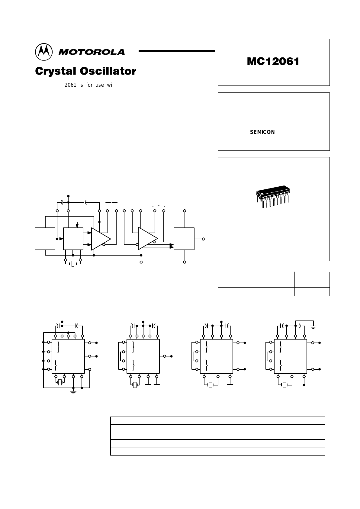
The MC12061 is for use with an external crystal to form a crystal
controlled oscillator. In addition to the fundamental series mode crystal, two
bypass capacitors are required (plus usual power supply pin bypass
capacitors). Translators are provided internally for MECL and TTL outputs.
• Frequency Range = 2.0 to 20 MHz
• Temperature Range = 0 to + 70°C
• Single Supply Operation: +5.0 Vdc or –5.2 Vdc
• Three Outputs Available:
1. Complementary Sine Wave (600 mVpp typ)
2. Complementary MECL
3. Single Ended TTL
Figure 1. Block Diagram
Note: 0.1 µF power supply
pin bypass capacitors
not shown.
Voltage
Reg.
Bias
Bypass
0.1
µ
F
AGC
Filter
0.1
µ
F
V
CC
Sine Wave
Output
MECL
Output
71 VCC4 3 2 141516 VCC13 12 11 V
CC
Crystal
Osc.
AGC
Ampl./
AGC
Sine
to
MECL
MECL
to
TTL
Trans-
lator
10
TTL
Output
–+
–+
56
Crystal
8V
EE
VEE9
TYPICAL CIRCUIT CONFIGURATIONS
Note: 0.1 µF power supply pin bypass capacitors not shown.
Figure 2. Sine Wave
Output
Figure 3. MTTL Output Figure 4. MECL Output
(+5.0 V Supply)
Figure 5. MECL Output
(–5.2 V Supply)
111617
+5.0 V
4
3–
2+
Sine
Out
MECL Out
In
14
15
12
13
658 9
10
+
–
111617
+5.0 V
4
10
TTL
Out
In
Out
2
3
14
15
6589
+
–
–
+
1617
+5.0 V
4
In
Out
2
3
14
15
658
+
–
–
+
13 +
12 –
MECL
Out
16174
In
Out
2
3
14
15
658
+
–
–
+
13 +
12 –
MECL
Out
–5.2 V
Characteristic MC12061
Mode of Operation Fundamental Series Resonance
Frequency Range 2.0 MHz — 20 MHz
Series Resistance, R1 Minimum at Fundamental
Maximum Effective Resistance R
E(max)
155 ohms
Motorola, Inc. 1997 Rev 5
Note: Start-up stabilization
time is a function of
crystal series resistance. The lower the
resistance, the faster
the circuit stabilizes.
CRYSTAL
REQUIREMENTS
MC12061
2
MOTOROLA RF/IF DEVICE DATA
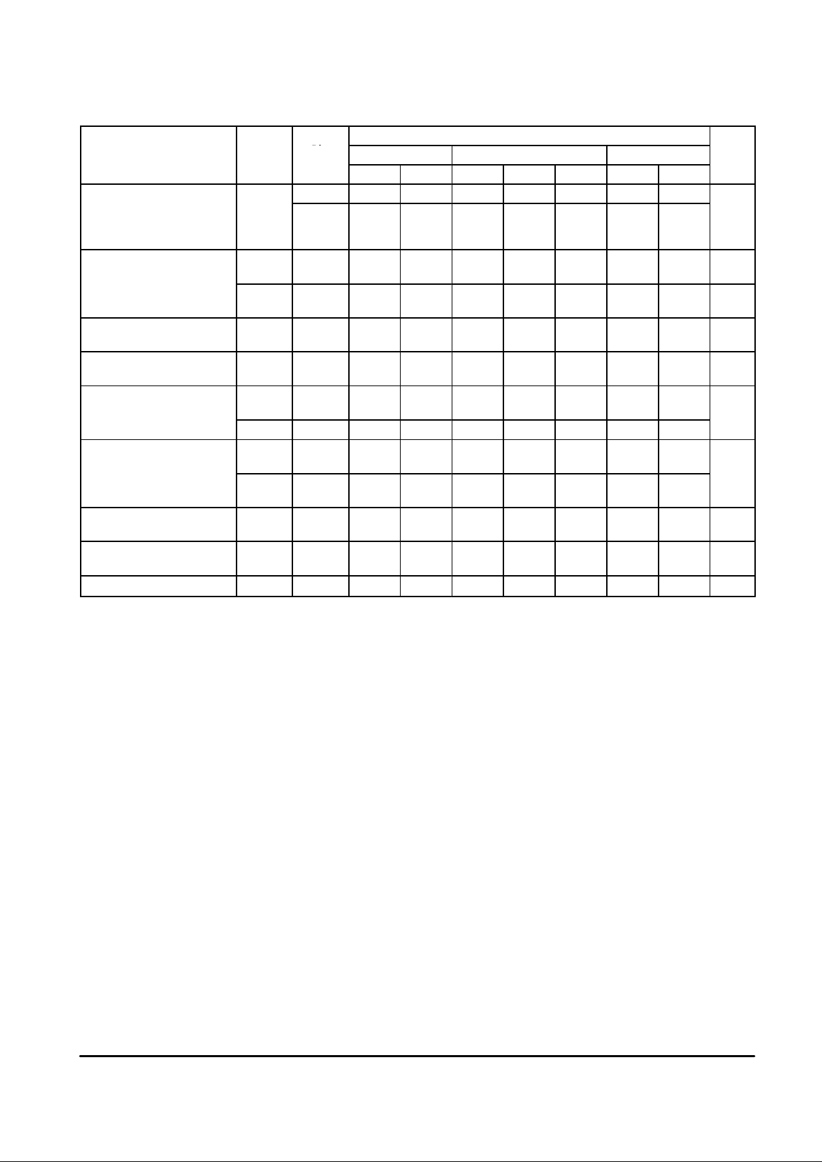
ELECTRICAL CHARACTERISTICS
Test Limits
Pin
Under
0°C +25°C +75°C
Characteristic Symbol
Under
Test
Min Max Min Typ Max Min Max
Unit
Power Supply Drain Current
I
CC
1 – – 13 16 19 – – mAdc
pp y
1
11
16
–
–
–
–
–
–
18
–
13
23
3.0
16
28
4.0
19
–
–
–
–
–
–
Input Current I
inH
14
15
–
–
–
–
–
–
–
–
250
250
–
–
–
–
µAdc
I
inL
14
15
–
–
–
–
–
–
–
–
1.0
1.0
–
–
–
–
µAdc
Differential Offset V oltage ∆V 4 to 7
2 to 3
–
–
–
–
40
–200
–
0
325
+200
–
–
–
–
mAdc
Output Voltage Level V
out
2
3
–
–
–
–
–
–
3.5
3.5
–
–
–
–
–
–
Vdc
Logic ‘1’ Output Voltage V
OH1
(Note 1)
12
13
4.0
4.0
4.16
4.16
4.04
4.04
–
–
4.19
4.19
4.1
4.1
4.28
4.28
Vdc
V
OH2
10 2.4 – 2.4 – – 2.4 –
Logic ‘0’ Output Voltage V
OL1
(Note 1)
12
13
2.98
2.98
3.43
3.43
3.0
3.0
–
–
3.44
3.44
3.02
3.02
3.47
3.47
Vdc
V
OL2
10
10
–
–
0.5
0.5
–
–
–
–
0.5
0.5
–
–
0.5
0.5
Logic ‘1’ Threshold Voltage V
OHA
12
13
3.98
3.98
–
–
4.02
4.02
–
–
–
–
4.08
4.08
–
–
Vdc
Logic ‘0’ Threshold Voltage V
OLA
12
13
–
–
3.45
3.45
–
–
–
–
3.46
3.46
–
–
3.49
3.49
Vdc
Output Short Circuit Current I
OS
10 20 60 20 – 60 20 60 mAdc
NOTE: 1. Devices will meet standard MECL logic levels using VEE = –5.2 Vdc and VCC = 0.
MC12061
3
MOTOROLA RF/IF DEVICE DATA
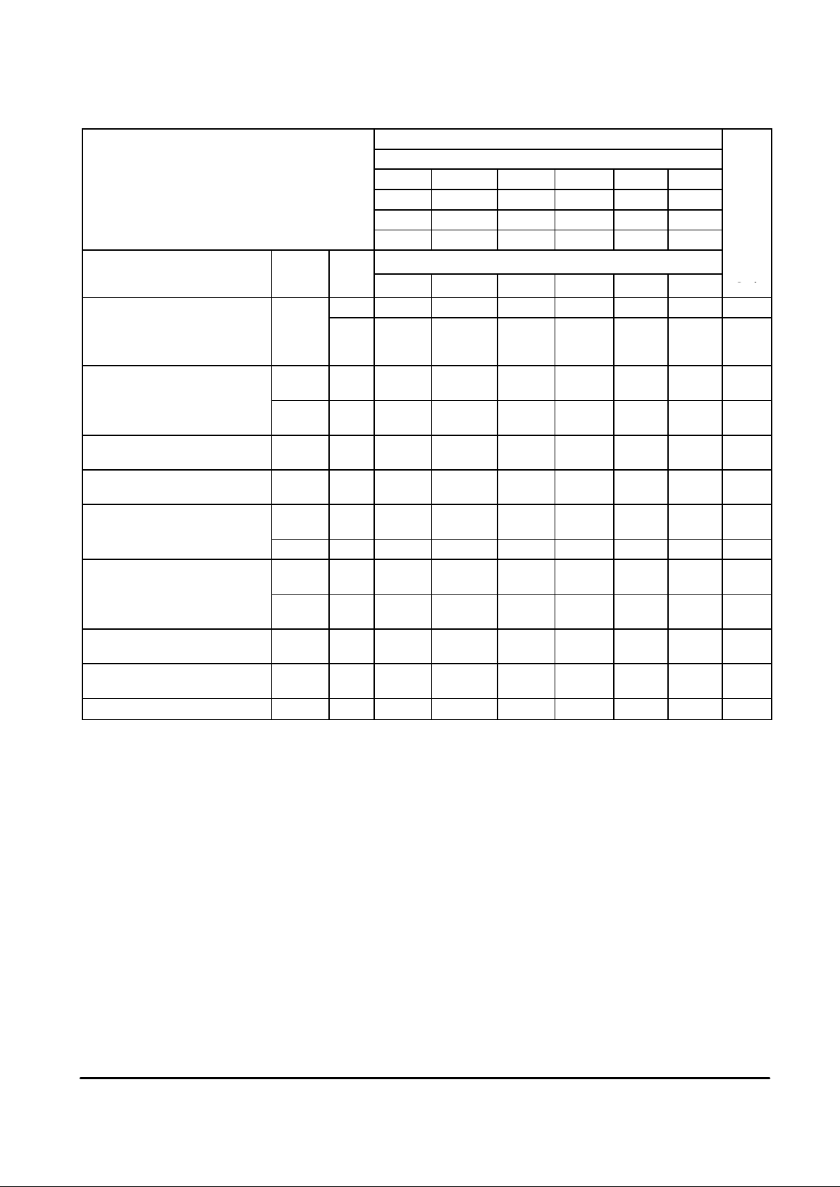
ELECTRICAL CHARACTERISTICS (continued)
TEST VOLTAGE/CURRENT VALUES
Volts
@ Test Temperature V
IHmax
V
ILminVIHAminVILAmax
V
IHT
V
CCL
0°C 4.16 3.19 3.86 3.51 4.0 4.75
+25°C 4.19 3.21 3.90 3.52 4.0 4.75
+75°C 4.28 3.23 3.96 3.55 4.0 4.75
Pin
TEST VOLTAGE APPLIED TO PINS LISTED BELOW
Characteristic Symbol
Und
er
Test
V
IHmax
V
ILminVIHAminVILAmax
V
IHT
V
CCL
Gnd
Power Supply Drain Current I
CC
1 – – – – – – 8
1
11
16
–
14
–
–
15
–
–
–
–
–
–
–
–
–
–
–
–
–
8
8,9
8
Input Current I
inH
14
15
14
15
15
14
–
–
–
–
–
–
–
–
8
8
I
inL
14
15
15
14
–
–
–
–
–
–
–
–
–
–
8,14
8,15
Differential Offset V oltage ∆V 4 to 7
2 to 3
–
–
–
–
–
–
–
–
5,6
4
–
–
8
–
Output Voltage Level V
out
2
3
–
–
–
–
–
–
–
–
4
4
–
–
8
8
Logic ‘1’ Output Voltage V
OH1
(Note 1)1213
14
15
15
14
–
–
–
–
–
–
–
–
8
8
V
OH2
10 15 14 – – – 11,16 8,9
Logic ‘0’ Output Voltage V
OL1
(Note 1)1213
15
14
14
15
–
–
–
–
–
–
–
–
8
8
V
OL2
10
10
14
14
15
15
–
–
–
–
–
–
11,16
–
8,9
8,9
Logic ‘1’ Threshold Voltage V
OHA
12
13
–
–
–
–
14
15
15
14
–
–
–
–
8
8
Logic ‘0’ Threshold Voltage V
OLA
12
13
–
–
–
–
15
14
14
15
–
–
–
–
8
8
Output Short Circuit Current I
OS
10 15 14 – – – 11,16 8,9,10
NOTE: 1. Devices will meet standard MECL logic levels using VEE = –5.2Vdc and VCC = 0.
 Loading...