

Motorola MC12058D, MC12058SD Datasheet
Order this document by MC12058/D
SEMICONDUCTOR
TECHNICAL DATA
MECL PLL COMPONENTS
÷126/128, ÷254/256
LOW POWER
DUAL MODULUS PRESCALER
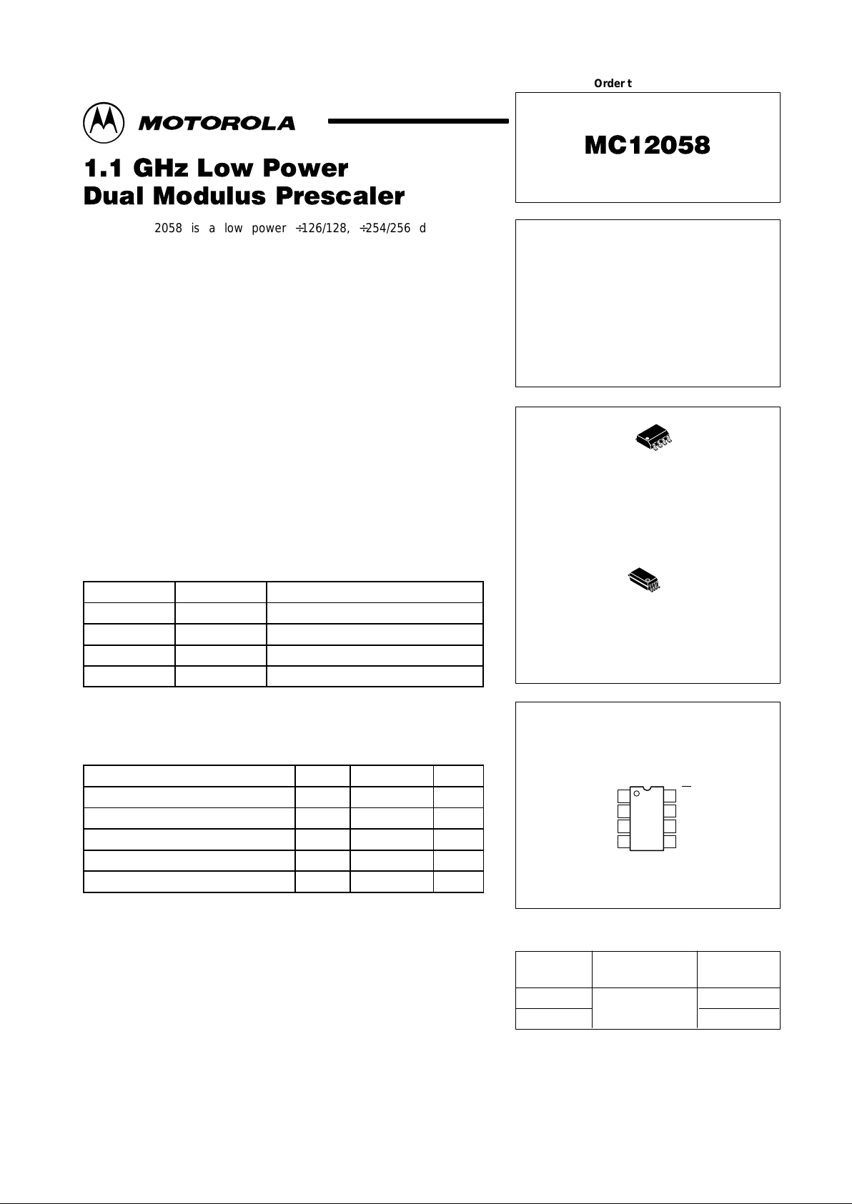
SD SUFFIX
PLASTIC PACKAGE
CASE 940
(SSOP–8)
PIN CONNECTIONS
D SUFFIX
PLASTIC PACKAGE
CASE 751
(SO–8)
8
1
1
8
IN
(Top View)
8
IN
V
CC
SW
OUT
NC
MC
Gnd
7
6
5
1
2
3
4
Device
Operating
Temp Range
Package
ORDERING INFORMATION
MC12058D
MC12058SD
TA = – 40° to +85°C
SO–8
SSOP–8
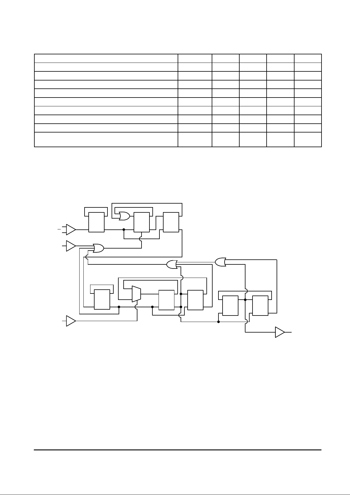
The MC12058 is a low power ÷126/128, ÷254/256 dual modulus
prescaler. Motorola’ s advanced Bipolar MOSAIC V technology is utilized to
achieve low power dissipation of 3.0 mW at a minimum supply voltage of
2.7 V. The MC12058 can be operated down to a minimum supply voltage of
2.7 V required for battery operated portable systems.
On–chip output termination provides 250 µA (typical) output current to
drive a 8.0 pF (typical) high impedance load. The Divide Ratio Control input,
SW, permits selection of divide ratio as desired. A HIGH on SW selects
÷126/128; an OPEN on SW selects ÷254/256. The Modulus Control input,
MC, selects the proper divide number after SW has been biased to select the
desired divide ratio.
• 1.1 GHz Toggle Frequency
• Supply Voltage 2.7 to 5.5 V
• Low Power 1.1 mA Typical at V
CC
= 3.0 V
• Operating Temperature Range of –40 to 85°C
• On–Chip Output Termination
MOSAIC V is a trademark of Motorola
FUNCTIONAL TABLE
SW MC Divide Ratio
H H 126
H L 128
L H 254
L L 256
NOTES: 1. SW: H = VCC, L = Open. A logic L can also be applied by grounding this pin,
but this is not recommended due to increased power consumption.
2.MC: H = 2.0 V to VCC, L = GND to 0.8 V.
MAXIMUM RATINGS
Characteristic Symbol Range Unit
Power Supply Voltage, Pin 2 V
CC
–0.5 to 7.0 Vdc
Operating Temperature Range T
A
–40 to 85 °C
Storage Temperature Range T
stg
–65 to 150 °C
Modulus Control Input, Pin 6 MC –0.5 to V
CC
Vdc
Maximum Output Current, Pin 4 I
O
4.0 mA
NOTE: ESD data available upon request.
Motorola, Inc. 1997 Rev 4
MC12058
2
MOTOROLA RF/IF DEVICE DATA
ELECTRICAL CHARACTERISTICS (VCC = 2.7 to 5.5 V; TA = –40 to 85°C, unless otherwise noted.)
Characteristic Symbol Min Typ Max Unit
Toggle Frequency (Sine Wave Input) f
t
0.1 1.4 1.1 GHz
Supply Current Output (Pin 2) I
CC
– 1.1 2.0 mA
Modulus Control Input HIGH (MC) V
IH1
2.0 – VCC + 0.5 V
Modulus Control Input LOW (MC) V
IL1
Gnd – 0.8 V
Divide Ratio Control Input HIGH (SW) V
IH2
VCC – 0.5 V
CC
VCC + 0.5 V
Divide Ratio Control Input LOW (SW) V
IH2
Open Open Open –
Output Voltage Swing (Note 1) V
out
0.8 1.1 – V
pp
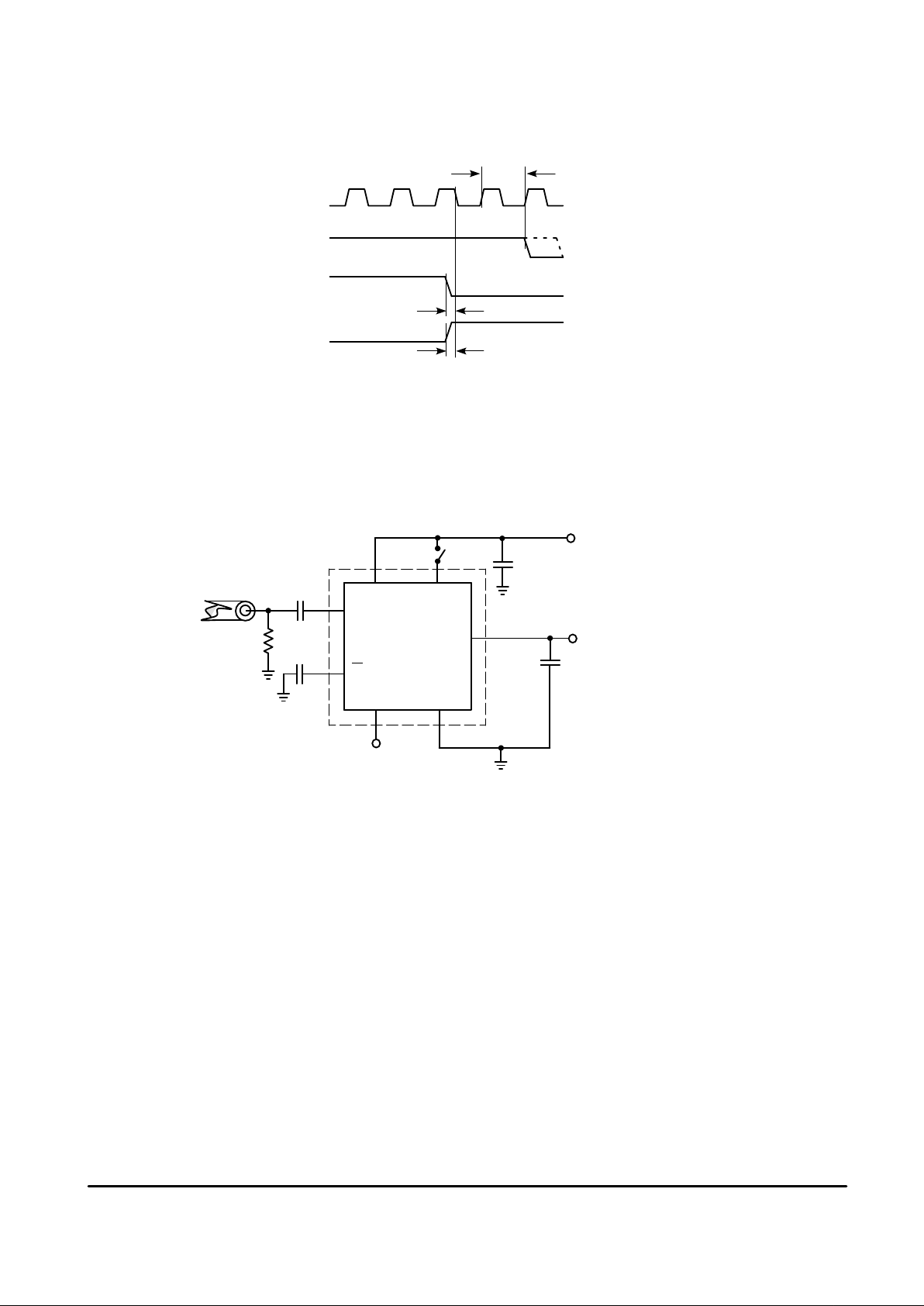
Modulus Setup Time MC to OUT at 1100 MHz t
set
– 11 16 ns
Input Voltage Sensitivity 250–1100 MHz
100–250 MHz
V
in
100
400
–
–
1000
1000
mVpp
NOTE: Assumes 8.0 pF high impedance load.
Figure 1. Logic Diagram (MC12058)
DQB
CQ
In
In
DQB
CQM
DQB
CQ
MC
DQB
CQ
1
0
DQB
CQ
DQB
CQ
SW
DQ
CQB
DQB
CQ
Out
MC12058
3
MOTOROLA RF/IF DEVICE DATA
Figure 2. Modulus Setup Time
Modulus setup time MC to out is the MC
setup or MC release plus the prop delay.
Prop. Delay
In
Out
MC
MC Setup
MC Release
Figure 3. AC Test Circuit
EXTERNAL COMPONENTS
C1 = C2 = 1000 pF
C3 = 0.1
µ
F
CL = 8.0 pF (Including Scope
and jig capacitance)
C
L
MC Input
C2
C1
C3
VCC = 2.7 to 5.5 V
50
Ω
Sine Wave Generator
SWV
CC
OUT
GND
MC
IN
IN
 Loading...