

Motorola MC10H424FN, MC10H424FNR2, MC10H424L, MC10H424P Datasheet
pp y
SEMICONDUCTOR TECHNICAL DATA
The MC10H424 is a Quad TTL–to–ECL translator with an ECL strobe.
Power supply requirements are ground, +5.0 volts, and –5.2 volts.
• Propagation Delay, 1.5 ns Typical
• Improved Noise Margin 150 mV (Over Operating Voltage and
Temperature Range)
• Voltage Compensated
• MECL 10K — Compatible
MAXIMUM RATINGS
Characteristic Symbol Rating Unit
Power Supply (VCC = 5.0 V) V
Power Supply (VEE = – 5.2 V) V
Input Voltage (ECL) V
Input Voltage (TTL) V
Output Current — Continuous
— Surge
Operating T emperature Range T
Storage T emperature Range — Plastic
— Ceramic
EE
CC
I
I
I
out
A
T
stg
ELECTRICAL CHARACTERISTICS (VEE = –5.2 V ± 5%, VCC = 5.0 V ± 5.0%)
0° 25° 75°
Characteristic Symbol Min Max Min Max Min Max Unit
Negative Power Supply
Drain Current
Positive Power Supply
Drain Current
Reverse Current Pin
5,7,10,1 1
Forward Current Pin
5,7,10,1 1
Input HIGH Current Pin 6 I
Input LOW Current Pin 6 I
Input Breakdown Voltage V
Input Clamp Voltage V
High Output Voltage V
Low Output Voltage V
High Input Voltage Pin
5,7,10,1 1
Low Input Voltage Pin
5,7,10,1 1
High Input Voltage Pin 6 V
Low Input Voltage Pin 6 V
I
E
I
CCH
I
CCL
I
R
I
F
inH
inL
(BR)in
I
OH
OL
V
IH
V
IL
IH
IL
— 72 — 66 — 72 mAdc
— 16 — 16 — 18 mAdc
— 25 — 25 — 25 mAdc
— 50 — 50 — 50 µAdc
— –3.2 — –3.2 — –3.2 mAdc
— 450 — 310 — 310 µAdc
0.5 — 0.5 — 0.3 — µAdc
5.5 — 5.5 — 5.5 — Vdc
— –1.5 — –1.5 — –1.5 Vdc
–1.02 –0.84 –0.98 –0.81 –0.92 –0.735 Vdc
–1.95 –1.63 –1.95 –1.63 –1.95 –1.60 Vdc
2.0 — 2.0 — +2.0 — Vdc
— 0.8 — 0.8 — 0.8 Vdc
–1.17 –0.84 –1.13 –0.81 –1.07 –0.735 Vdc
–1.95 –1.48 –1.95 –1.48 –1.95 –1.45 Vdc
–8.0 to 0 Vdc
0 to +7.0 Vdc
0 to V
EE
0 to V
CC
50
100
0 to +75 °C
–55 to +150
–55 to +165
Vdc
Vdc
mA
°C
CERAMIC PACKAGE
PLASTIC PACKAGE
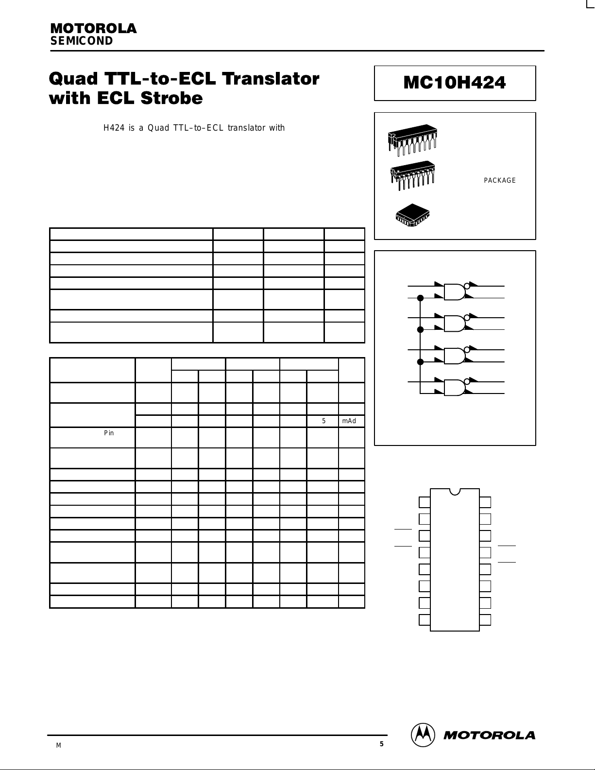
LOGIC DIAGRAM
5
6
7
10
11
GND = PIN 16
DIP
1
2
3
4
5
6
7
8
B
OUT
A
OUT
B
OUT
A
OUT
A
IN
COMMON
STROBE
B
IN
V
EE
VCC (+5.0 VDC) = PIN 9
VEE (–5.2 VDC) = PIN 8
PIN ASSIGNMENT
L SUFFIX
CASE 620–10
P SUFFIX
CASE 648–08
FN SUFFIX
PLCC
CASE 775–02
16
15
14
13
12
11
10
GND
C
D
D
C
D
C
V
9
4
2
3
1
12
15
13
14
OUT
OUT
OUT
OUT
IN
IN
CC
3/93
Motorola, Inc. 1996
2–117
Pin assignment is for Dual–in–Line Package.
For PLCC pin assignment, see the Pin Conversion
T ables on page 6–11 of the Motorola MECL Data
Book (DL122/D).
REV 5

MC10H424
AC PARAMETERS
Propagation Delay
Data
Strobe
Rise Time tr0.5 2.0 0.5 2.0 0.5 2.2 ns
Fall Time tf0.5 2.0 0.5 2.0 0.5 2.2 ns
t
pd
0.5
2.2
0.5
2.3
0.5
2.2
0.5
2.3
0.5
0.5
ns
2.4
2.4
APPLICATIONS INFORMATION
The MC10H424 has TTL–compatible inputs, an ECL strobe
and MECL complementary open–emitter outputs that allow
use as an inverting/non–inverting translator or as a differential
line driver. When the common strobe input is at the low–logic
level, it forces all true outputs to a MECL low–logic state and
NOTE:
Each MECL 10H series circuit has been designed to meet the dc specifications
shown in the test table, after thermal equilibrium has been established. The
circuit is in a test socket or mounted on a printed circuit board and transverse
air flow greater than 500 Ifpm is maintained. Outputs are terminated through
a 50–ohm resistor to –2.1 volts.
all inverting outputs to a MECL high–logic state.
An advantage of this device is that TTL–level information
can be transmitted differentially, via balanced twisted pair
lines, to MECL equipment, where the signal can be received
by the MC10H1 15 or MC10H116 differential line receivers.
MOTOROLA MECL Data
2–118
DL122 — Rev 6
 Loading...