

MOTOROLA MC10H352P, MC10H352FNR2 Datasheet
pp y
SEMICONDUCTOR TECHNICAL DATA
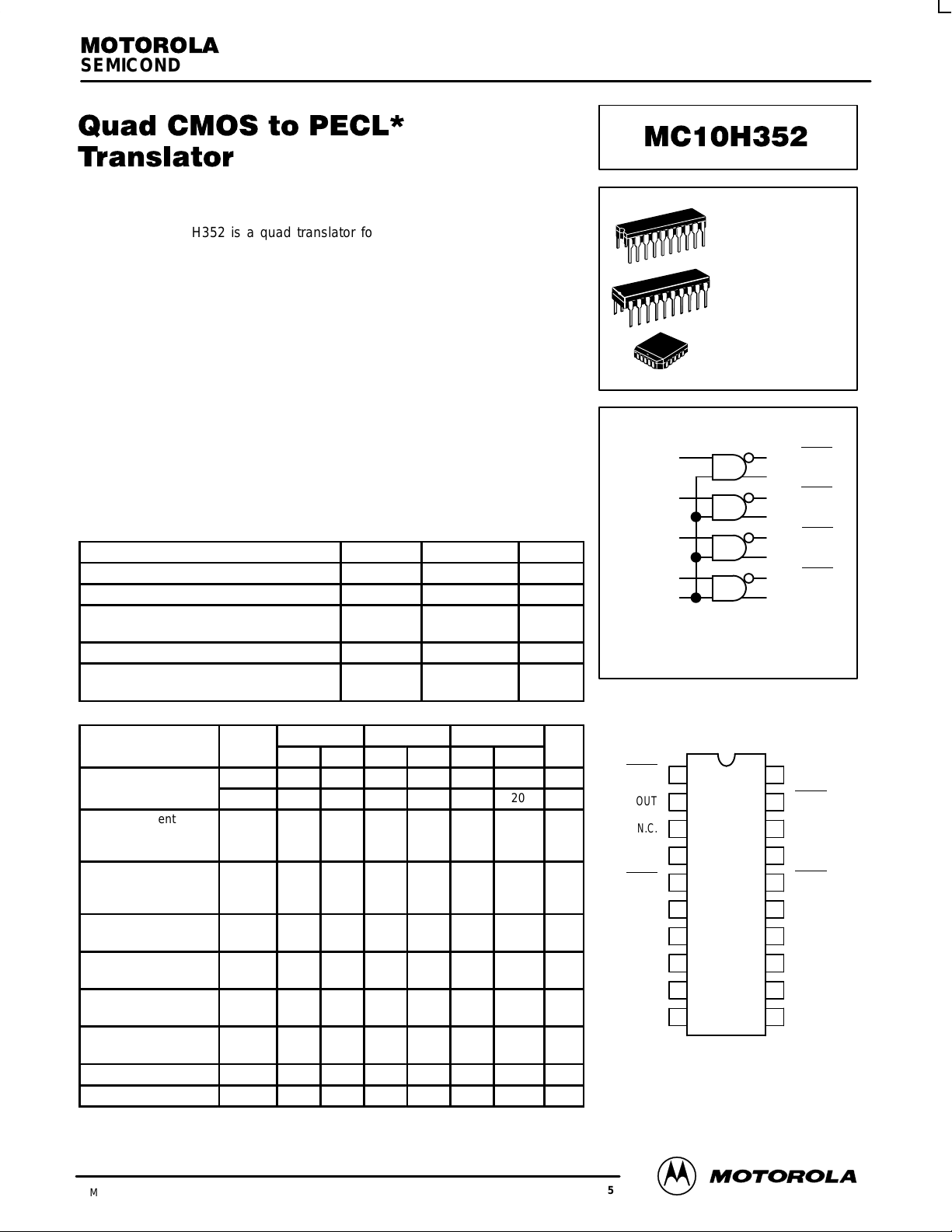
The MC10H352 is a quad translator for interfacing data between a
CMOS logic section and the PECL section of digital systems when only a
+5.0 Vdc power supply is available. The MC10H352 has CMOS
compatible inputs and PECL complementary open–emitter outputs that
allow use as an inverting/non–inverting translator or as a differential line
driver. When the common strobe input is at a low logic level, it forces all
true outputs to the PECL low logic state (≈ +3.2 V) and all inverting
outputs to the PECL high logic state (≈ +4.1 V).
The MC10H352 can also be used with the MC10H350 to transmit and
receive CMOS information differentially via balanced twisted pair lines.
• Single +5.0 V Power Supply
• All VCC Pins Isolated On Chip
• Differentially Drive Balanced Lines
• tpd = 1.3 nsec Typical
MAXIMUM RATINGS
Characteristic Symbol Rating Unit
Power Supply V
Input Voltage (VCC = 5.0 V) V
Output Current— Continuous
Operating Temperature Range T
Storage Temperature Range— Plastic
— Surge
— Ceramic
ELECTRICAL CHARACTERISTICS (VCC = V
0° 25° 75°
Characteristic Symbol Min Max Min Max Min Max Unit
Power Supply
Current
Reverse Current
Pins 7, 8, 12, 14
Pin 9
Forward Current
Pins 7, 8, 12, 14
Pin 9
Input Voltage
Breakdown
Input Clamp Voltage
(Iin = –18 mA)
High Output
Voltage (1)
Low Output
Voltage (1)
High Input Voltage V
Low Input Voltage V
(1) With VCC at 5.0 V. VOH/VOL change 1:1 with VCC.
*Positive Emitter Coupled Logic
ECL — 50 — 45 — 50 mA
TTL — 20 — 15 — 20 mA
I
V
(BR)in
V
V
R
I
F
V
OH
OL
IH
——25
——–0.8
5.5 — 5.5 — 5.5 — Vdc
— –1.5 — –1.5 — –1.5 Vdc
I
3.98 4.16 4.02 4.19 4.08 4.27 Vdc
3.05 3.37 3.05 3.37 3.05 3.37 Vdc
3.15 — 3.15 — 3.15 — Vdc
— 1.5 — 1.5 — 1.5 Vdc
IL
CC
I
I
out
A
T
stg
CC1
100——2080——25100
–3.2——
0 to +7.0 Vdc
0 to V
50
100
0 to +75 °C
–55 to +150
–55 to +165
= V
= 5.0 V ± 5.0%)
CC2
–0.6
–2.4——
CC
–0.8
–3.2
Vdc
mA
°C
µA
mA
L SUFFIX
CERAMIC PACKAGE
CASE 732–03
P SUFFIX
PLASTIC PACKAGE
CASE 738–03
FN SUFFIX
PLCC
CASE 775–02
LOGIC DIAGRAM
71
B IN
8
A IN
12
D IN
14 19
C IN
COMMON
STROBE
9
VCC (+5.0 VDC) = PINS 6, 11, 15, 20
GND = PIN 10
DIP
PIN ASSIGNMENT
B OUT
B OUT
N.C.
A OUT
A OUT
V
CC
B IN
A IN
COMMON
STROBE
GND
Pin assignment is for Dual–in–Line Package.
For PLCC pin assignment, see the Pin Conversion
Tables on page 6–36 of the Motorola MECL Data
1
2
3
4
5
6
7
8
9
10
Book (DL122/D).
20
19
18
17
16
15
14
13
12
11
B OUT
B OUT
2
5
A OUT
A OUT
4
16
D OUT
D OUT
17
C OUT
18
C OUT
ECL V
CC
C OUT
C OUT
D OUT
D OUT
VCC 2
C IN
N.C.
D IN
CMOS V
CC
3/93
Motorola, Inc. 1996
2–96
REV 5
MC10H352
AC PARAMETERS
0° 25° 75°
Characteristic Symbol Min Max Min Max Min Max Unit
Propagation Delay (1) t
Rise Time (20% to 80%) t
Fall Time (80% to 20%) t
Maximum Operating Frequency f
(1) Propagation delay is measured on this circuit from VCC/2 on the input waveform to the 50% point on the output waveform.
NOTE:
Each MECL 10H series circuit has been designed to meet the dc specifications shown in the test table, after thermal equilibrium has been established. The
circuit is in a test socket or mounted on a printed circuit board and transverse air flow greater than 500 lfpm is maintained. Outputs are terminated through
a 50–ohm resistor to VCC – 2.0 Vdc.
pd
r
f
max
0.4 1.9 0.4 2.0 0.4 2.1 ns
0.4 1.9 0.4 2.0 0.4 2.1 ns
0.4 1.9 0.4 2.0 0.4 2.1 ns
150 — 150 — 150 — MHz
DL122 — Rev 6
2–97 MOTOROLAMECL Data
 Loading...