

SEMICONDUCTOR TECHNICAL DATA
The MC10H210 is designed to drive up to six transmission lines simultan–
eously. The multiple outputs of this device also allow the wire “OR”–ing of
several levels of gating for minimization of gate and package count.
The ability to control three parallel lines with minimum propagation delay
from a single point makes the MC10H210 particularly useful in clock distribution
applications where minimum clock skew is desired.
• Propagation Delay Average, 1.0 ns T ypical
• Power Dissipation, 160 mW Typical
• Improved Noise Margin 150 mV (Over Operating Voltage and
Temperature Range)
• Voltage Compensated
• MECL 10K–Compatible
MAXIMUM RATINGS
Characteristic Symbol Rating Unit
Power Supply (VCC = 0) V
Input Voltage (VCC = 0) V
Output Current— Continuous
— Surge
Operating Temperature Range T
Storage Temperature Range— Plastic
— Ceramic
T
I
EE
I
out
A
stg
ELECTRICAL CHARACTERISTICS (VEE = –5.2 V ±5%) (See Note)
0° 25° 75°
Characteristic Symbol Min Max Min Max Min Max Unit
Power Supply Current I
Input Current High I
Input Current Low I
High Output Voltage V
Low Output Voltage V
High Input Voltage V
Low Input Voltage V
E
inH
inL
OH
OL
IH
— 42 — 38 — 42 mA
— 720 — 450 — 450 µA
0.5 — 0.5 — 0.3 — µA
–1.02 –0.84 –0.98 –0.81 –0.92 –0.735 Vdc
–1.95 –1.63 –1.95 –1.63 –1.95 –1.60 Vdc
–1.17 –0.84 –1.13 –0.81 –1.07 –0.735 Vdc
–1.95 –1.48 –1.95 –1.48 –1.95 –1.45 Vdc
IL
AC PARAMETERS
Propagation Delay t
Rise Time t
Fall Time t
NOTE:
Each MECL 10H series circuit has been designed to meet the dc specifications shown in the test table,
after thermal equilibrium has been established. The circuit is in a test socket or mounted on a printed
circuit board and transverse air flow greater than 500 Iinear fpm is maintained. Outputs are terminated
through a 50–ohm resistor to –2.0 volts.
Note: If crosstalk is present, double bypass capacitor to 0.2 µF.
pd
0.5 1.55 0.55 1.55 0.6 1.7 ns
0.75 1.8 0.75 1.9 0.8 2.0 ns
r
0.75 1.8 0.75 1.9 0.8 2.0 ns
f
–8.0 to 0 Vdc
0 to V
EE
50
100
0 to +75 °C
–55 to +150
–55 to +165
Vdc
mA
°C
°C
L SUFFIX
CERAMIC PACKAGE
CASE 620–10
P SUFFIX
PLASTIC PACKAGE
CASE 648–08
FN SUFFIX
PLCC
CASE 775–02
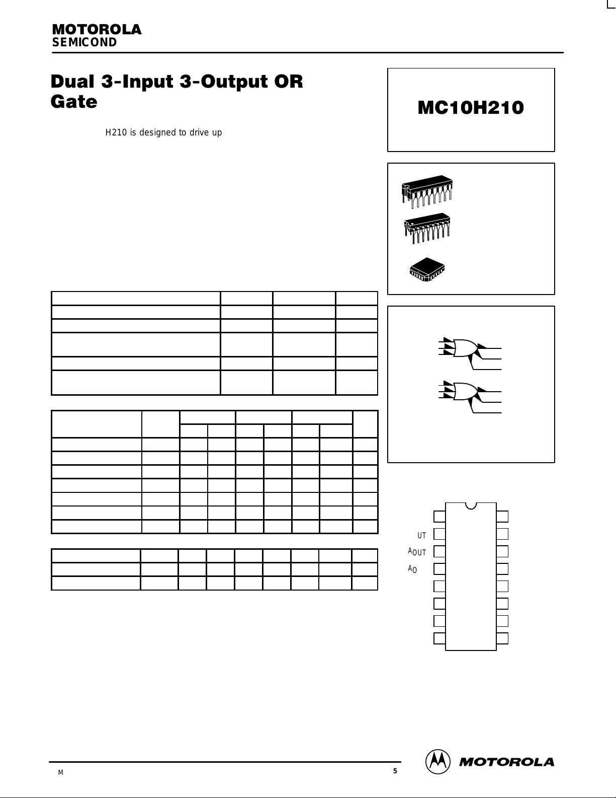
LOGIC DIAGRAM
5
6
7
9
10
11
V
= PINS 1, 15
CC1
V
= PIN 16
CC2
VEE = PIN 8
DIP
PIN ASSIGNMENT
V
A
OUT
A
OUT
A
OUT
CC1
A
IN
A
IN
A
IN
V
EE
1
2
3
4
5
6
7
8
16
15
14
13
12
11
10
9
2
3
4
12
13
14
V
CC2
V
CC1
B
OUT
B
OUT
B
OUT
B
IN
B
IN
B
IN
3/93
Motorola, Inc. 1996
2–293
Pin assignment is for Dual–in–Line Package.
For PLCC pin assignment, see the Pin Conversion
T ables on page 6–11 of the Motorola MECL Data
Book (DL122/D).
REV 5
MC10H210
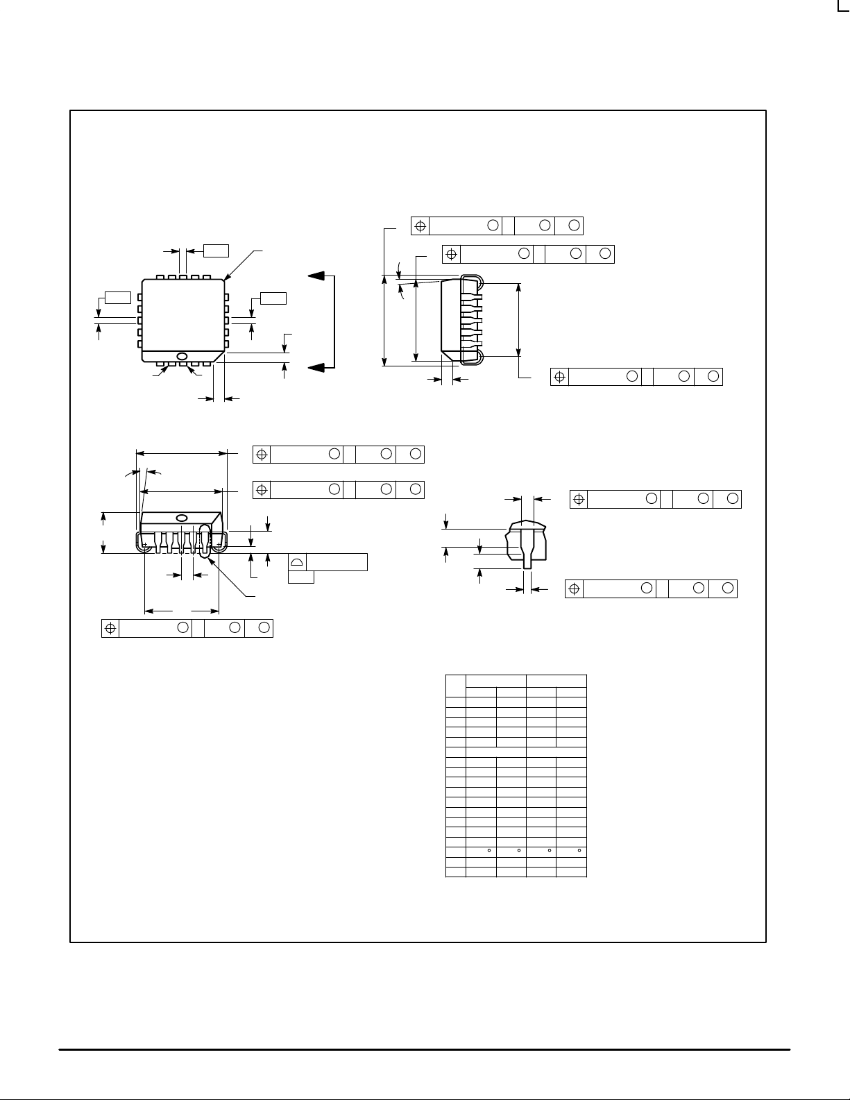
OUTLINE DIMENSIONS
FN SUFFIX
PLASTIC PLCC PACKAGE
CASE 775–02
ISSUE C
–L–
20 1
Z
C
G
G1
0.010 (0.250) N
S
T
–N–
L–M
S
Y BRK
–M–
W
V
A
0.007 (0.180) N
0.007 (0.180) N
R
E
0.004 (0.100)
J
PLANE
SEATING
–T–
VIEW S
S
0.007 (0.180) N
B
0.007 (0.180) N
U
M
S
L–M
T
M
S
S
L–M
T
S
D
Z
D
X
0.010 (0.250) N
G1
S
S
L–M
T
S
VIEW D–D
M
M
S
L–M
T
L–M
T
S
S
S
0.007 (0.180) N
H
M
S
L–M
T
S
K1
K
0.007 (0.180) N
F
M
S
L–M
T
S
VIEW S
NOTES:
1. DATUMS –L–, –M–, AND –N– DETERMINED
WHERE TOP OF LEAD SHOULDER EXITS PLASTIC
BODY AT MOLD PARTING LINE.
2. DIMENSION G1, TRUE POSITION TO BE
MEASURED AT DA TUM –T–, SEATING PLANE.
3. DIMENSIONS R AND U DO NOT INCLUDE MOLD
FLASH. ALLOWABLE MOLD FLASH IS 0.010 (0.250)
PER SIDE.
4. DIMENSIONING AND TOLERANCING PER ANSI
Y14.5M, 1982.
5. CONTROLLING DIMENSION: INCH.
6. THE PACKAGE TOP MAY BE SMALLER THAN THE
PACKAGE BOTTOM BY UP TO 0.012 (0.300).
DIMENSIONS R AND U ARE DETERMINED AT THE
OUTERMOST EXTREMES OF THE PLASTIC BODY
EXCLUSIVE OF MOLD FLASH, TIE BAR BURRS,
GATE BURRS AND INTERLEAD FLASH, BUT
INCLUDING ANY MISMATCH BETWEEN THE TOP
AND BOTTOM OF THE PLASTIC BODY.
7. DIMENSION H DOES NOT INCLUDE DAMBAR
PROTRUSION OR INTRUSION. THE DAMBAR
PROTRUSION(S) SHALL NOT CAUSE THE H
DIMENSION TO BE GREATER THAN 0.037 (0.940).
THE DAMBAR INTRUSION(S) SHALL NOT CAUSE
THE H DIMENSION TO BE SMALLER THAN 0.025
(0.635).
MOTOROLA MECL Data
DIM MIN MAX MIN MAX
A 0.385 0.395 9.78 10.03
B 0.385 0.395 9.78 10.03
C 0.165 0.180 4.20 4.57
E 0.090 0.110 2.29 2.79
F 0.013 0.019 0.33 0.48
G 0.050 BSC 1.27 BSC
H 0.026 0.032 0.66 0.81
J 0.020 ––– 0.51 –––
K 0.025 ––– 0.64 –––
R 0.350 0.356 8.89 9.04
U 0.350 0.356 8.89 9.04
V 0.042 0.048 1.07 1.21
W 0.042 0.048 1.07 1.21
X 0.042 0.056 1.07 1.42
Y ––– 0.020 ––– 0.50
Z 2 10 2 10
____
G1 0.310 0.330 7.88 8.38
K1 0.040 ––– 1.02 –––
2–294
MILLIMETERSINCHES
DL122 — Rev 6
 Loading...