

MOTOROLA MC10H188P, MC10H188MEL, MC10H188ML1, MC10H188ML2, MC10H188MR1 Datasheet
...
SEMICONDUCTOR TECHNICAL DATA
2–284
REV 5
Motorola, Inc. 1996
3/93
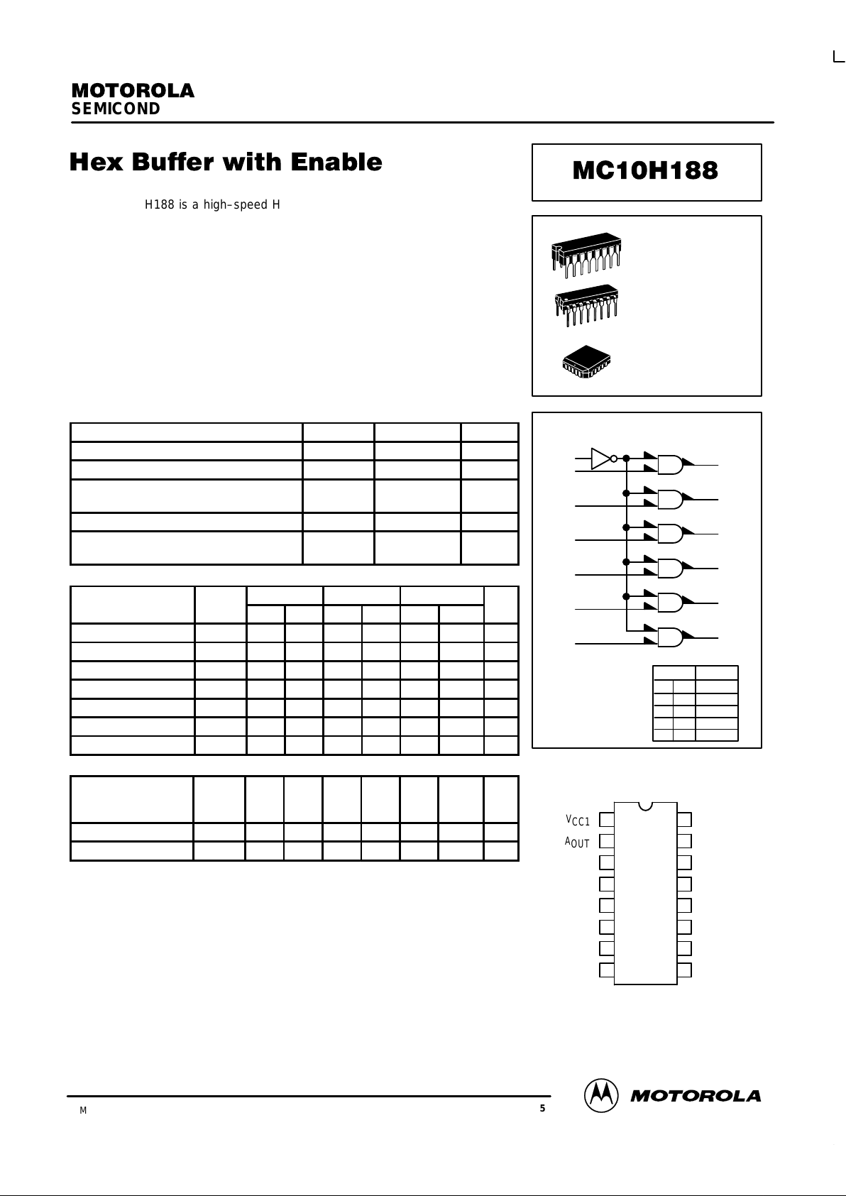
The MC10H188 is a high–speed Hex Buffer with a common Enable input.
When Enable is in the high–state, all outputs are in the low–state. When Enable
is in the low–state, the outputs take the same state as the inputs.
This MECL 10H part is a functional/pinout duplication of the standard MECL
10K family part, with 100% improvement in propagation delay and no increase
in power–supply current.
• Propagation Delay, 1.3 ns Typical Data–to–Output
• Power Dissipation 180 mW Typ/Pkg (No Load)
• Improved Noise Margin 150 mV (Over Operating Voltage and
Temperature Range)
• Voltage Compensated
• MECL 10K–Compatible
MAXIMUM RATINGS
Characteristic Symbol Rating Unit
Power Supply (VCC = 0) V
EE
–8.0 to 0 Vdc
Input Voltage (VCC = 0) V
I
0 to V
EE
Vdc
Output Current— Continuous
— Surge
I
out
50
100
mA
Operating Temperature Range T
A
0 to +75 °C
Storage Temperature Range— Plastic
— Ceramic
T
stg
–55 to +150
–55 to +165
°C
°C
ELECTRICAL CHARACTERISTICS (VEE = –5.2 V ±5%) (See Note)
0° 25° 75°
Characteristic Symbol Min Max Min Max Min Max Unit
Power Supply Current I
E
— 46 — 42 — 46 mA
Input Current High I
inH
— 495 — 310 — 310 µA
Input Current Low I
inL
0.5 — 0.5 — 0.3 — µA
High Output Voltage V
OH
–1.02 –0.84 –0.98 –0.81 –0.92 –0.735 Vdc
Low Output Voltage V
OL
–1.95 –1.63 –1.95 –1.63 –1.95 –1.60 Vdc
High Input Voltage V
IH
–1.17 –0.84 –1.13 –0.81 –1.07 –0.735 Vdc
Low Input Voltage V
IL
–1.95 –1.48 –1.95 –1.48 –1.95 –1.45 Vdc
AC PARAMETERS
Propagation Delay
Enable
Data
t
pd
0.7
0.7
2.2
1.9
0.7
0.7
2.2
1.9
0.7
0.7
2.2
1.9
ns
Rise Time t
r
0.7 2.4 0.7 2.4 0.7 2.4 ns
Fall Time t
f
0.7 2.4 0.7 2.4 0.7 2.4 ns
NOTE:
Each MECL 10H series circuit has been designed to meet the dc specifications shown in the test table,
after thermal equilibrium has been established. The circuit is in a test socket or mounted on a printed circuit
board and transverse air flow greater than 500 Ifpm is maintained. Outputs are terminated through a
50–ohm resistor to –2.0 volts.
X Y OUT
Inputs Output
LOGIC DIAGRAM
DIP
PIN ASSIGNMENT
V
CC1
A
OUT
B
OUT
C
OUT
A
IN
B
IN
C
IN
V
EE
V
CC2
F
OUT
E
OUT
D
OUT
F
IN
E
IN
D
IN
COMMON
16
15
14
13
12
11
10
9
1
2
3
4
5
6
7
8
V
CC1
= Pin 1
V
CC2
= Pin 16
VEE = Pin 8
TRUTH TABLE
12
15
11
14
10
13
7
4
6
3
5
2
9
X
Y
OUT
L
L
H
H
L
H
L
H
L
H
L
L
L SUFFIX
CERAMIC PACKAGE
CASE 620–10
P SUFFIX
PLASTIC PACKAGE
CASE 648–08
FN SUFFIX
PLCC
CASE 775–02
Pin assignment is for Dual–in–Line Package.
For PLCC pin assignment, see the Pin Conversion
T ables on page 6–11 of the Motorola MECL Data
Book (DL122/D).
MC10H188
2–285 MOTOROLAMECL Data
DL122 — Rev 6
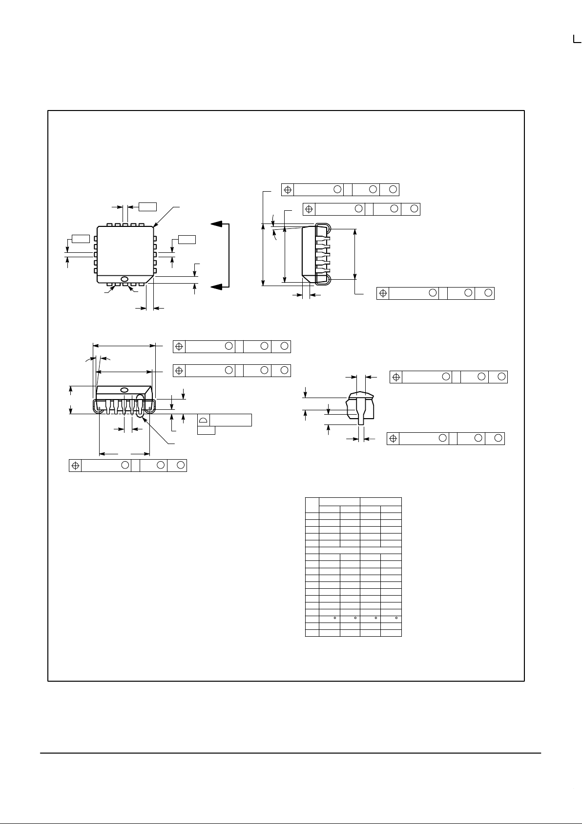
OUTLINE DIMENSIONS
FN SUFFIX
PLASTIC PLCC PACKAGE
CASE 775–02
ISSUE C
NOTES:
1. DATUMS –L–, –M–, AND –N– DETERMINED
WHERE TOP OF LEAD SHOULDER EXITS PLASTIC
BODY AT MOLD PARTING LINE.
2. DIMENSION G1, TRUE POSITION TO BE
MEASURED AT DATUM –T–, SEATING PLANE.
3. DIMENSIONS R AND U DO NOT INCLUDE MOLD
FLASH. ALLOWABLE MOLD FLASH IS 0.010 (0.250)
PER SIDE.
4. DIMENSIONING AND TOLERANCING PER ANSI
Y14.5M, 1982.
5. CONTROLLING DIMENSION: INCH.
6. THE PACKAGE TOP MAY BE SMALLER THAN THE
PACKAGE BOTTOM BY UP TO 0.012 (0.300).
DIMENSIONS R AND U ARE DETERMINED AT THE
OUTERMOST EXTREMES OF THE PLASTIC BODY
EXCLUSIVE OF MOLD FLASH, TIE BAR BURRS,
GATE BURRS AND INTERLEAD FLASH, BUT
INCLUDING ANY MISMATCH BETWEEN THE TOP
AND BOTTOM OF THE PLASTIC BODY.
7. DIMENSION H DOES NOT INCLUDE DAMBAR
PROTRUSION OR INTRUSION. THE DAMBAR
PROTRUSION(S) SHALL NOT CAUSE THE H
DIMENSION TO BE GREATER THAN 0.037 (0.940).
THE DAMBAR INTRUSION(S) SHALL NOT CAUSE
THE H DIMENSION TO BE SMALLER THAN 0.025
(0.635).
–M–
–N–
–L–
Y BRK
W
V
D
D
S
L–M
M
0.007 (0.180) N
S
T
S
L–M
M
0.007 (0.180) N
S
T
S
L–M
S
0.010 (0.250) N
S
T
X
G1
B
U
Z
VIEW D–D
20 1
S
L–M
M
0.007 (0.180) N
S
T
S
L–M
M
0.007 (0.180) N
S
T
S
L–M
S
0.010 (0.250) N
S
T
C
G
VIEW S
E
J
R
Z
A
0.004 (0.100)
–T–
SEATING
PLANE
S
L–M
M
0.007 (0.180) N
S
T
S
L–M
M
0.007 (0.180) N
S
T
H
VIEW S
K
K1
F
G1
DIM MIN MAX MIN MAX
MILLIMETERSINCHES
A 0.385 0.395 9.78 10.03
B 0.385 0.395 9.78 10.03
C 0.165 0.180 4.20 4.57
E 0.090 0.110 2.29 2.79
F 0.013 0.019 0.33 0.48
G 0.050 BSC 1.27 BSC
H 0.026 0.032 0.66 0.81
J 0.020 ––– 0.51 –––
K 0.025 ––– 0.64 –––
R 0.350 0.356 8.89 9.04
U 0.350 0.356 8.89 9.04
V 0.042 0.048 1.07 1.21
W 0.042 0.048 1.07 1.21
X 0.042 0.056 1.07 1.42
Y ––– 0.020 ––– 0.50
Z 2 10 2 10
G1 0.310 0.330 7.88 8.38
K1 0.040 ––– 1.02 –––
____
 Loading...