

Motorola MC10H180L, MC10H180P, MC10H180FN Datasheet
SEMICONDUCTOR TECHNICAL DATA
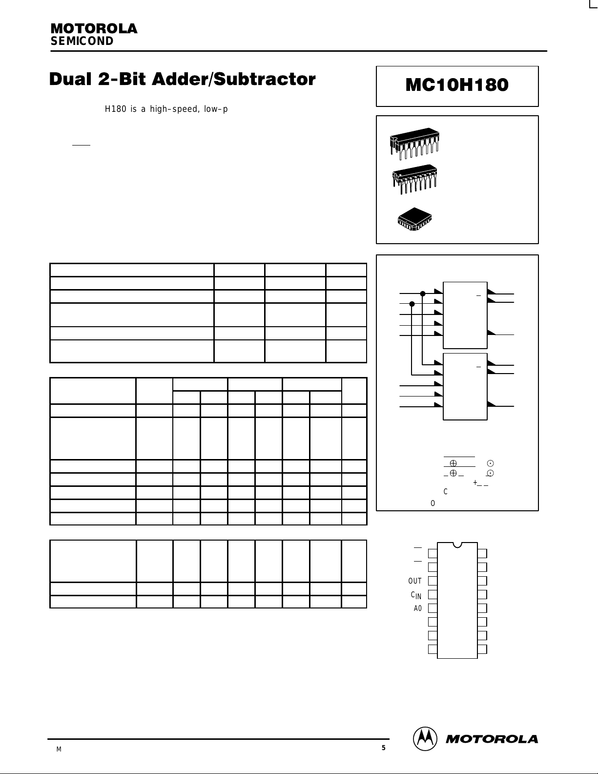
The MC10H180 is a high–speed, low–power, general–purpose adder/
subtractor. It is designed to be used in special purpose adders/subtractors or in
high–speed multiplier arrays.
Inputs for each adder are Carry–in, Operand A, and Operand B; outputs are
Sum, Sum
Invert A for subtract, and a control line to Invert B.
MAXIMUM RATINGS
Power Supply (VCC = 0) V
Input Voltage (VCC = 0) V
Output Current— Continuous
Operating Temperature Range T
Storage Temperature Range— Plastic
ELECTRICAL CHARACTERISTICS (VEE = –5.2 V ±5%) (See Note)
Power Supply Current I
Input Current High
Pins 4, 12
Pins 7, 9
Pins 5, 6, 10, 11
Input Current Low I
High Output Voltage V
Low Output Voltage V
High Input Voltage (1) V
Low Input Voltage (1) V
AC PARAMETERS
Propagation Delay
Operand to Output
Select to Output
Carry–in to Output
Rise Time t
Fall Time t
NOTES:
Each MECL 10H series circuit has been designed to meet the dc specifications shown in the test table,
after thermal equilibrium has been established. The circuit is in a test socket or mounted on a printed circuit
board and transverse air flow greater than 500 Ifpm is maintained. Outputs are terminated through a
50–ohm resistor to –2.0 volts.
and Carry–out. The common select inputs serve as a control line to
• Propagation Delay, 1.8 ns Typical, Operand and Select to Output
• Power Dissipation, 360 mW Typical
• Improved Noise Margin 150 mV (Over Operating Voltage and
Temperature Range)
• Voltage Compensated
• MECL 10K–Compatible
Characteristic Symbol Rating Unit
EE
I
I
665
515
410
2.4
2.2
1.6
T
out
A
stg
—
—
—
0.7
0.7
0.4
— Surge
— Ceramic
0° 25° 75°
Characteristic Symbol Min Max Min Max Min Max Unit
— 95 — 86 — 95 mA
—
—
—
0.5 — 0.5 — 0.3 — µA
–1.02 –0.84 –0.98 –0.81 –0.92 –0.735 Vdc
–1.95 –1.63 –1.95 –1.63 –1.95 –1.60 Vdc
–1.17 –0.84 –1.13 –0.81 –1.07 –0.735 Vdc
–1.95 –1.48 –1.95 –1.48 –1.95 –1.45 Vdc
IL
0.6
0.6
0.4
0.5 2.0 0.5 2.1 0.5 2.2 ns
r
0.5 2.0 0.5 2.1 0.5 2.2 ns
f
I
E
inH
inL
OH
OL
IH
t
pd
–8.0 to 0 Vdc
0 to V
EE
50
100
0 to +75 °C
–55 to +150
–55 to +165
417
320
255
2.5
2.3
1.7
—
—
—
0.8
0.8
0.4
Vdc
mA
°C
°C
417
320
255
2.8
2.6
1.8
µA
ns
L SUFFIX
CERAMIC PACKAGE
CASE 620–10
P SUFFIX
PLASTIC PACKAGE
CASE 648–08
FN SUFFIX
PLCC
CASE 775–02
LOGIC DIAGRAM
7
9
5
6
4
11
10
12
S1
S0
COUT
C
IN
A0
B0
SEL
V
EE
Pin assignment is for Dual–in–Line Package.
For PLCC pin assignment, see the Pin Conversion
T ables on page 6–11 of the Motorola MECL Data
SEL
SEL
AO
BO
C
SEL
SEL
A1
B1
C
POSITIVE LOGIC ONLY
A’ = A
B’ = B
S=C
CIN(A’ B’ + A’
C
= CINA’ + CINB’ + A’ B’
OUT
S0
A
S
0
B
C
OUT
IN
S1
A
1
S
B
C
OUT
IN
VCC = PIN 16
VEE = PIN 8
SELA = ASEL
SELB = BSEL
(A’ B’ + A’ B’) +
IN
B’)
DIP
PIN ASSIGNMENT
1
16
2
15
3
14
4
13
5
12
6
11
7
A
Book (DL122/D).
10
8
9
V
CC
S0
S1
C
OUT
C
IN
A1
B1
SEL
15
2
3
14
1
13
A
B
B
3/93
Motorola, Inc. 1996
2–271
REV 5
MC10H180
FUNCTION SELECT TABLE TRUTH TABLE
SelASel
H S = A plus B
H
L
L
B
H
L
S = A minus B
H
S = B minus A
L
S = 0 minus A minus B
Function
FUNCTION
ADD
SUBTRACT
INPUTS
SelASelBA0 B0 CinS0 S0
H
H
H
H
H
H
H
H
H
H
H
H
H
H
H
H
L
L
H
L
L
H
H
L
H
H
L
H
L
H
H
L
H
H
H
H
H
H
H
H
L
L
L
L
L
L
H
L
L
H
L
L
L
H
L
L
H
L
H
H
L
H
H
L
L
L
H
H
H
L
L
H
H
L
L
H
L
L
H
H
H
L
L
H
L
L
H
H
L
L
H
H
H
L
L
H
C
H
L
L
H
L
H
H
L
L
H
H
L
H
L
L
H
out
L
L
L
H
L
H
H
H
L
H
L
L
H
H
L
H
FUNCTION
REVERSE
SUBTRACT
INPUTS
SelASelBA0 B0 CinS0 S0
L
L
L
L
L
L
L
L
L
L
L
L
L
L
L
L
L
L
H
L
L
H
H
L
H
H
L
H
L
H
H
L
H
H
H
H
H
H
H
H
L
L
L
L
L
L
H
L
L
H
L
L
L
H
L
L
H
L
H
H
L
H
H
L
H
L
L
H
L
L
H
H
L
L
H
H
H
L
L
H
L
L
H
H
H
L
L
H
H
L
L
H
L
L
H
H
C
out
L
L
H
H
H
H
H
L
L
H
L
L
L
L
H
H
H
H
H
L
L
L
H
H
L
L
H
H
L
H
L
L
MOTOROLA MECL Data
2–272
DL122 — Rev 6
 Loading...