

MOTOROLA MC10H164FNR2, MC10H164M, MC10H164FN, MC10H164MEL, MC10H164ML1 Datasheet
...
SEMICONDUCTOR TECHNICAL DATA
2–257
REV 6
Motorola, Inc. 1996
9/96
The MC10H164 is a MECL 10H part which is a functional/pinout duplication
of the standard MECL 10K family part, with 100% improvement in propagation
delay , and no increase in power supply current.
The MC10H164 is designed to be used in data multiplexing and parallel to
serial conversion applications. Full parallel gating provides equal delays
through any data path. The MC10H164 incorporates an output buffer, eight
inputs and an enable. A high on the enable forces the output low. The open
emitter output allows the MC10H164 to be connected directly to a data bus. The
enable line allows an easy means of expanding to more than 8 lines using
additional MC10H164’s.
• Propagation Delay, 1.0 ns Typical
• Power Dissipation, 310 mW Typical (same as MECL 10K)
• Improved Noise Margin 150 mV (Over Operating Voltage and
Temperature Range)
• Voltage Compensated
• MECL 10K–Compatible
MAXIMUM RATINGS
Characteristic Symbol Rating Unit
Power Supply (VCC = 0) V
EE
–8.0 to 0 Vdc
Input Voltage (VCC = 0) V
I
0 to V
EE
Vdc
Output Current— Continuous
— Surge
I
out
50
100
mA
Operating Temperature Range T
A
0 to +75 °C
Storage Temperature Range— Plastic
— Ceramic
T
stg
–55 to +150
–55 to +165
°C
°C
ELECTRICAL CHARACTERISTICS (VEE = –5.2 V ±5%) (See Note)
0° 25° 75°
Characteristic Symbol Min Max Min Max Min Max Unit
Power Supply Current I
E
— 83 — 75 — 83 mA
Input Current High I
inH
— 512 — 320 — 320 µA
Input Current Low I
inL
0.7 — 0.7 — 0.7 — µA
High Output Voltage V
OH
–1.02 –0.84 –0.98 –0.81 –0.92 –0.735 Vdc
Low Output Voltage V
OL
–1.95 –1.63 –1.95 –1.63 –1.95 –1.60 Vdc
High Input Voltage V
IH
–1.17 –0.84 –1.13 –0.81 –1.07 –0.735 Vdc
Low Input Voltage V
IL
–1.95 –1.48 –1.95 –1.48 –1.95 –1.45 Vdc
AC PARAMETERS
Propagation Delay
Enable
Data
Address
t
pd
0.4
0.7
1.0
1.45
2.4
2.8
0.4
0.8
1.1
1.5
2.5
2.9
0.5
0.9
1.2
1.7
2.6
3.2
ns
Rise Time t
r
0.5 1.5 0.5 1.6 0.5 1.7 ns
Fall Time t
f
0.5 1.5 0.5 1.6 0.5 1.7 ns
NOTE:
Each MECL 10H series circuit has been designed to meet the dc specifications shown in the test table,
after thermal equilibrium has been established. The circuit is in a test socket or mounted on a printed circuit
board and transverse air flow greater than 500 Iinear fpm is maintained. Outputs are terminated through
a 50–ohm resistor to –2.0 volts.
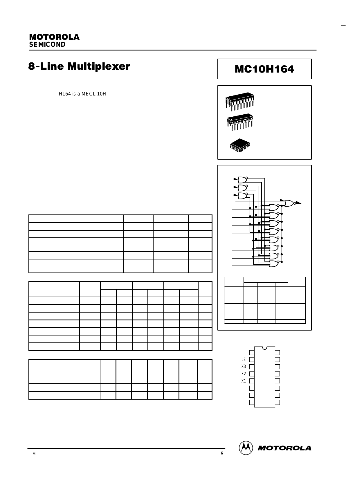
DIP PIN ASSIGNMENT
V
CC1
ENABLE
X3
X2
X1
X0
A
V
EE
V
CC2
Z
X7
X6
X5
X4
C
B
16
15
14
13
12
11
10
9
1
2
3
4
5
6
7
8
LOGIC DIAGRAM
V
CC1
= PIN 1
V
CC2
= PIN 16
VEE= PIN 8
A 7
B 9
C 10
Enable
2
X0 6
X1 5
X2 4
X3 3
X4 11
X5 12
X6 13
X7 14
Z
15
TRUTH TABLE
ADDRESS INPUTS
ENABLE
CBAZ
L
L
L
L
L
L
L
L
L
L
H
H
L
H
L
H
X0
X1
X2
X3
H
XLXX
L
L
L
L
H
H
H
H
L
L
H
H
L
H
L
H
X4
X5
X6
X7
L SUFFIX
CERAMIC PACKAGE
CASE 620–10
P SUFFIX
PLASTIC PACKAGE
CASE 648–08
FN SUFFIX
PLCC
CASE 775–02
Pin assignment is for Dual–in–Line Package.
For PLCC pin assignment, see the Pin Conversion
T ables on page 6–11 of the Motorola MECL Data
Book (DL122/D).
MC10H164
MOTOROLA MECL Data
DL122 — Rev 6
2–258
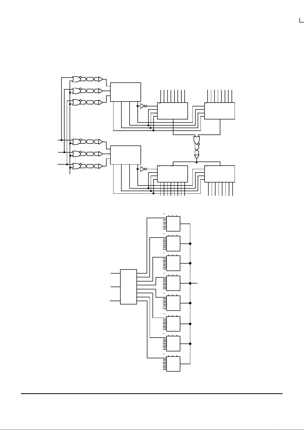
FIGURE 2 — 1–OF–64 LINE MULTIPLEXER
FIGURE 1 — HIGH SPEED 16–BIT
MULTIPLEXER/DEMULTIPLEXER
TYPICAL APPLICATIONS
The Bit chosen is dependent on six–bit
code present on inputs 7, 9, 14 of the
MC10H161 and the A, B, C inputs of the
MC10H164.
MC10H161
MC10H164
E
1
C
B
A
MC10H136
MC10H161
MC10H162
S0
S1
C
R
ABCD
E
1
C
B
A
E
0
MC10H164
765432
1
0
E
1
C
B
A
D0
Control Selection
MC10H136
MC10H164
S0
S1
C
R
ABCD
15 14 13 12 11 10 9 8
76543210
E
1
C
B
A
D0
Start/Stop
S0
15 141312 1110 9 8
E
0
S1
C
R
D
out
D
out
D
out
D
out
D
out
D
out
ABC
E
MC10H164
ABC
E
MC10H164
D
out
ABC
E
MC10H164
ABC
E
MC10H164
ABC
E
MC10H164
ABC
E
MC10H164
ABC
E
MC10H164
MC10H161
D
out
ABC
MSB
LSB
Q7
Q6
Q5
Q4
Q3
Q2
Q1
Q0
14
9
7
E
MC10H164
 Loading...