

Motorola MC10H161P, MC10H161FN, MC10H161L Datasheet
SEMICONDUCTOR TECHNICAL DATA
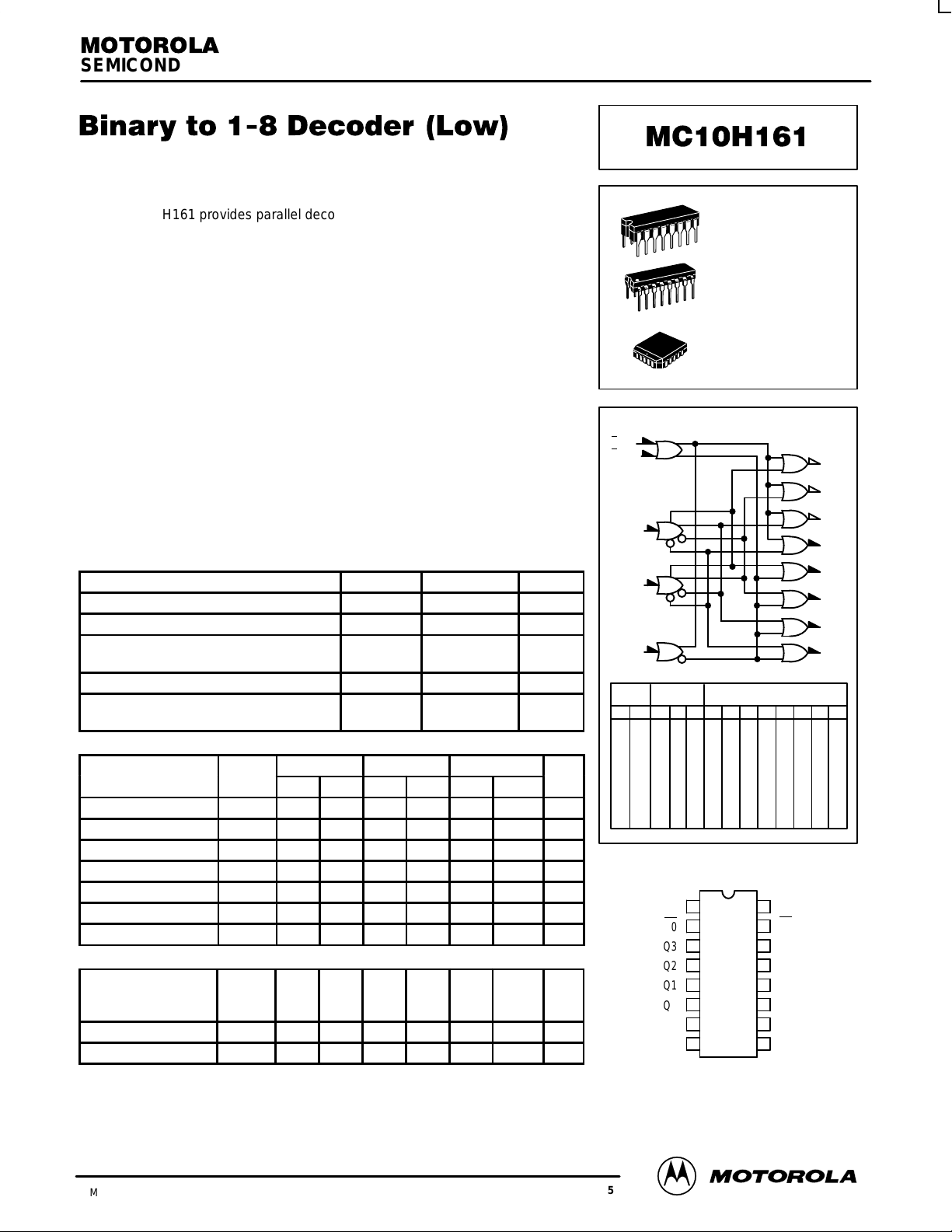
The MC10H161 provides parallel decoding of a three bit binary word to one
of eight lines. The MC10H161 is useful in high–speed multiplexer/demultiplexer
applications.
The MC10H161 is designed to decode a three bit input word to one of eight
output lines. The MC10H161 output will be low when selected while all other
output are high. The enable inputs, when either or both are high, force all
outputs high.
The MC10H161 is a true parallel decoder. This eliminates unequal parallel
path delay times found in other decoder designs. These devices are ideally
suited for multiplexer/demultiplexer applications.
• Propagation Delay, 1.0 ns Typical
• Power Dissipation, 315 mW Typical (same as MECL 10K)
• Improved Noise Margin 150 mV (Over Operating Voltage and
Temperature Range)
• Voltage Compensated
• MECL 10K–Compatible
MAXIMUM RATINGS
Characteristic Symbol Rating Unit
Power Supply (VCC = 0) V
Input Voltage (VCC = 0) V
Output Current— Continuous
— Surge
Operating Temperature Range T
Storage Temperature Range— Plastic
— Ceramic
T
I
EE
I
out
A
stg
ELECTRICAL CHARACTERISTICS (VEE = –5.2 V ±5%) (See Note)
0° 25° 75°
Characteristic Symbol Min Max Min Max Min Max Unit
Power Supply Current I
Input Current High I
Input Current Low I
High Output Voltage V
Low Output Voltage V
High Input Voltage V
Low Input Voltage V
E
inH
inL
OH
OL
IH
— 84 — 76 — 84 mA
— 465 — 275 — 275 µA
0.5 — 0.5 — 0.3 — µA
–1.02 –0.84 –0.98 –0.81 –0.92 –0.735 Vdc
–1.95 –1.63 –1.95 –1.63 –1.95 –1.60 Vdc
–1.17 –0.84 –1.13 –0.81 –1.07 –0.735 Vdc
–1.95 –1.48 –1.95 –1.48 –1.95 –1.45 Vdc
IL
AC PARAMETERS
Propagation Delay
Data
Enable
Rise Time t
Fall Time t
NOTE:
Each MECL 10H series circuit has been designed to meet the dc specifications shown in the test table,
after thermal equilibrium has been established. The circuit is in a test socket or mounted on a printed circuit
board and transverse air flow greater than 500 Iinear fpm is maintained. Outputs are terminated through
a 50–ohm resistor to –2.0 volts.
t
pd
0.6
2.0
2.3
0.65
0.8
0.8
0.55 1.7 0.65 1.8 0.7 1.9 ns
r
0.55 1.7 0.65 1.8 0.7 1.9 ns
f
–8.0 to 0 Vdc
0 to V
EE
50
100
0 to +75 °C
–55 to +150
–55 to +165
2.1
0.7
2.4
0.9
Vdc
mA
°C
°C
2.2
2.5
ns
L SUFFIX
CERAMIC PACKAGE
CASE 620–10
P SUFFIX
PLASTIC PACKAGE
CASE 648–08
FN SUFFIX
PLCC
CASE 775–02
LOGIC DIAGRAM
E02
E115
V
= Pin 1
CC1
V
= Pin 16
CC2
VEE= Pin 8
A7
B9
C14
ENABLE
INPUTS
L
L
L
L
L
L
L
L
H
X
L
L
L
L
L
L
L
L
X
H
TRUTH TABLE
INPUTS OUTPUTS
H
H
H
L
L
L
L
L
L
L
H
H
H
H
X
X
H
H
L
H
L
H
H
H
H
H
L
L
H
H
L
H
L
H
H
H
H
H
X
X
H
X
X
H
H
L
H
L
H
L
H
H
H
H
H
H
H
H
H
H
H
H
H
H
H
H
H
H
H
H
DIP
PIN ASSIGNMENT
1
V
CC1
E0
Q3
Q2
Q1
Q0
A
V
EE
Pin assignment is for Dual–in–Line Package.
For PLCC pin assignment, see the Pin Conversion
T ables on page 6–11 of the Motorola MECL Data
Book (DL122/D).
16
2
15
3
14
4
13
5
12
6
11
7
10
8
9
6Q0
5Q1
4Q2
3Q3
13 Q4
12 Q5
11 Q6
10 Q7
Q4E0E1 C B A Q0 Q1 Q2 Q3 Q5 Q6 Q7
H
H
H
H
H
H
H
H
H
H
H
H
H
H
L
H
L
H
L
H
H
H
H
H
H
H
H
H
H
H
V
CC2
E1
C
Q4
Q5
Q6
Q7
B
H
H
H
H
H
H
H
L
H
H
3/93
Motorola, Inc. 1996
2–249
REV 5
MC10H161
S0
TYPICAL APPLICATIONS
FIGURE 1 — HIGH SPEED 16–BIT MULTIPLEXER/DEMULTIPLEXER
Control Selection
S0
S1
MC10H136
C
R
ABCD
15 14 13 12 11 10 9 8
E1
C
MC10H164
B
A
D0
765432
E
1
C
B
A
MC10H164
D0
1
0
S1
C
R
Start/Stop
S0
S1
MC10H136
C
R
ABCD
E
0
1
E
C
MC10H161
B
A
15 141312 11 10 9 8
E0
E1
C
MC10H161
B
A
76543210
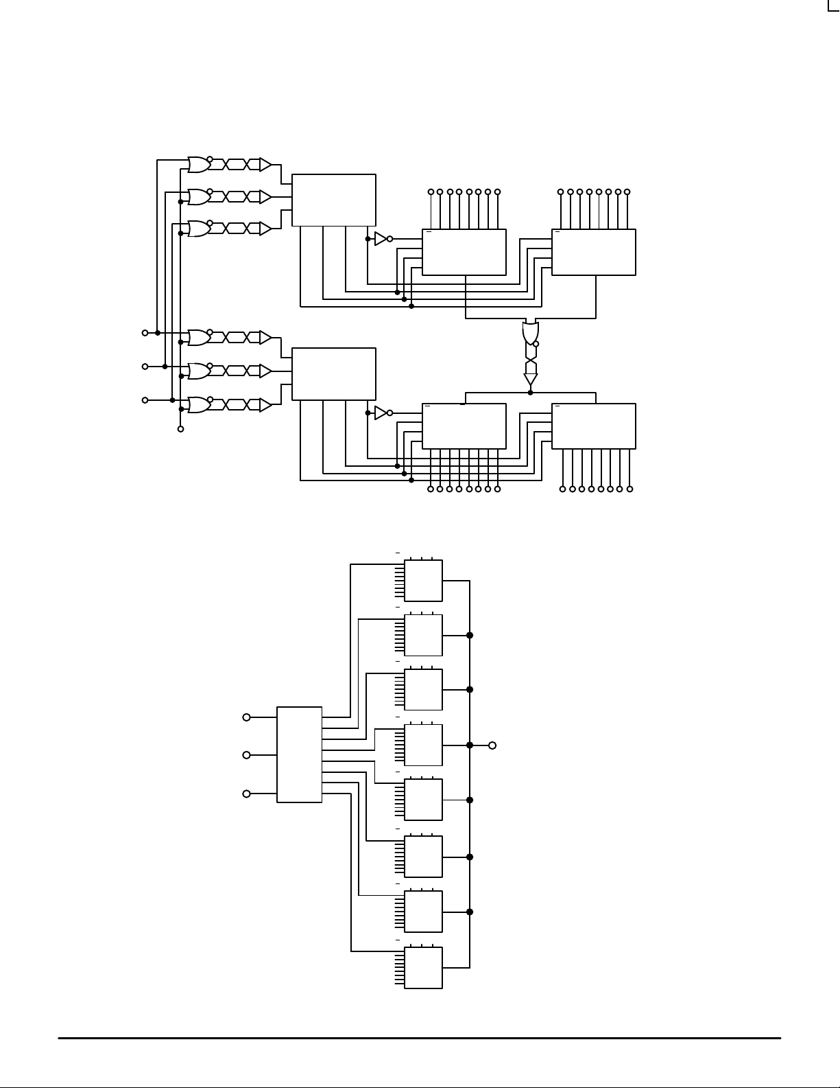
FIGURE 2 — 1–OF–64 LINE MULTIPLEXER
ABC
E
MC10H164
E
MC10H164
E
MC10H164
MSB
14
9
7
MC10H161
LSB
Q7
Q6
Q5
Q4
Q3
Q2
Q1
Q0
E
MC10H164
E
MC10H164
ABC
ABC
ABC
ABC
D
out
D
out
D
out
D
out
D
out
ABC
E
MC10H164
E
The Bit chosen is dependent on six–bit
code present on inputs 7, 9, 14 of the
MC10H161 and the A, B, C inputs of the
MC10H164.
MOTOROLA MECL Data
MC10H164
E
MC10H164
2–250
ABC
ABC
D
out
D
out
D
out
DL122 — Rev 6
 Loading...