

MOTOROLA MC10H159ML1, MC10H159ML2, MC10H159MR1, MC10H159MEL, MC10H159L Datasheet
...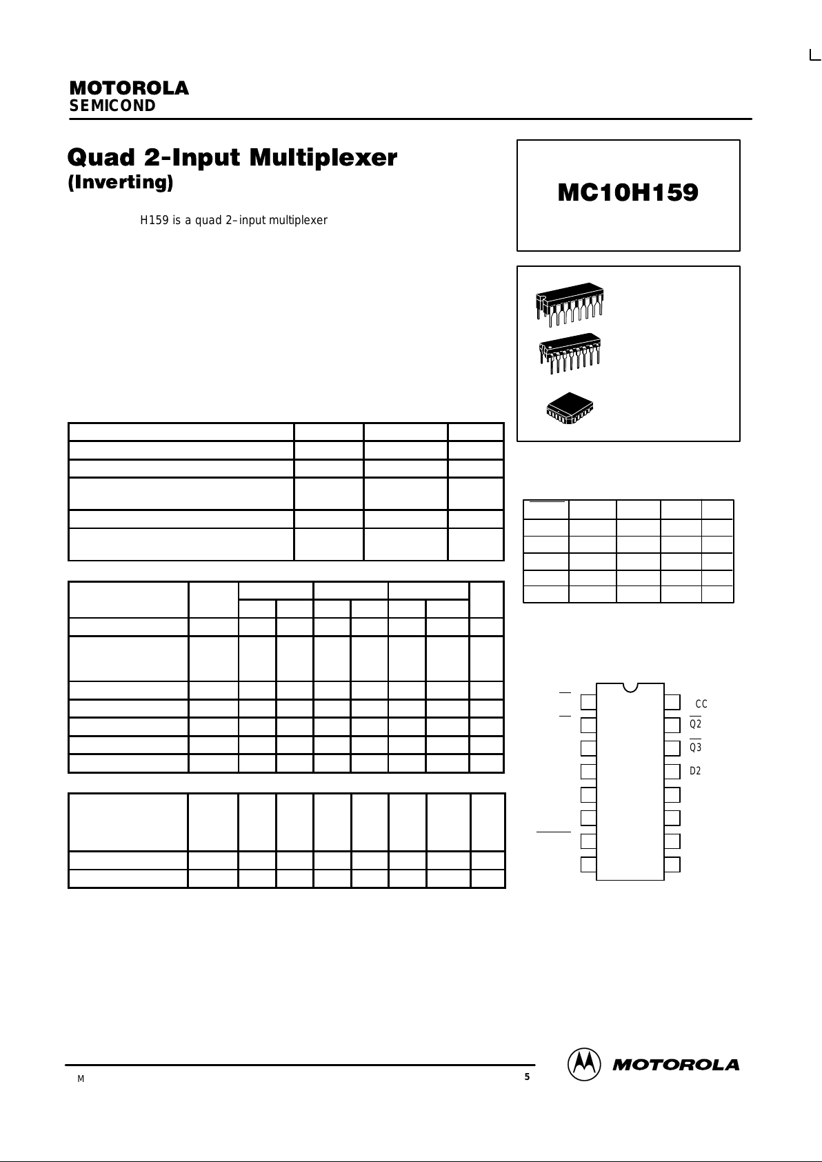
SEMICONDUCTOR TECHNICAL DATA
2–242
REV 5
Motorola, Inc. 1996
3/93
The MC10H159 is a quad 2–input multiplexer with enable. This MECL 10H
part is a functional/pinout duplication of the standard MECL 10K family part,
with 100% improvement in propagation delay and no increase in power–supply
current.
• Propagation Delay, 1.5 ns Typical
• Power Dissipation, 218 mW Typical
• Improved Noise Margin 150 mV (Over Operating Voltage and
Temperature Range)
• Voltage Compensated
• MECL 10K–Compatible
MAXIMUM RATINGS
Characteristic Symbol Rating Unit
Power Supply (VCC = 0) V
EE
–8.0 to 0 Vdc
Input Voltage (VCC = 0) V
I
0 to V
EE
Vdc
Output Current— Continuous
— Surge
I
out
50
100
mA
Operating Temperature Range T
A
0 to +75 °C
Storage Temperature Range— Plastic
— Ceramic
T
stg
–55 to +150
–55 to +165
°C
°C
ELECTRICAL CHARACTERISTICS (VEE = –5.2 V ±5%) (See Note)
0° 25° 75°
Characteristic Symbol Min Max Min Max Min Max Unit
Power Supply Current I
E
— 58 — 53 — 58 mA
Input Current High
Pin 9
Pins 3–7 and 10–13
I
inH
——475
515——
295
320——
295
320
µA
Input Current Low I
inL
0.5 — 0.5 — 0.3 — µA
High Output Voltage V
OH
–1.02 –0.84 –0.98 –0.81 –0.92 –0.735 Vdc
Low Output Voltage V
OL
–1.95 –1.63 –1.95 –1.63 –1.95 –1.60 Vdc
High Input Voltage V
IH
–1.17 –0.84 –1.13 –0.81 –1.07 –0.735 Vdc
Low Input Voltage V
IL
–1.95 –1.48 –1.95 –1.48 –1.95 –1.45 Vdc
AC PARAMETERS
Propagation Delay
Data
Select
Enable
t
pd
0.5
1.0
1.0
2.2
3.2
3.2
0.5
1.0
1.0
2.2
3.2
3.2
0.5
1.0
1.0
2.2
3.2
3.2
ns
Rise Time t
r
0.5 2.2 0.5 2.2 0.5 2.2 ns
Fall Time t
f
0.5 2.2 0.5 2.2 0.5 2.2 ns
NOTE:
Each MECL 10H series circuit has been designed to meet the dc specifications shown in the test table,
after thermal equilibrium has been established. The circuit is in a test socket or mounted on a printed circuit
board and transverse air flow greater than 500 Iinear fpm is maintained. Outputs are terminated through
a 50–ohm resistor to –2.0 volts.
TRUTH TABLE
DIP
PIN ASSIGNMENT
Q0
Q1
D11
D10
D01
D00
ENABLE
V
EE
V
CC
Q2
Q3
D20
D21
D30
D31
SELECT
16
15
14
13
12
11
10
9
1
2
3
4
5
6
7
8
Select D0 D1 QEnable
LL LHX
LL HLX
LH XHL
LH XLH
HX XLX
L SUFFIX
CERAMIC PACKAGE
CASE 620–10
P SUFFIX
PLASTIC PACKAGE
CASE 648–08
FN SUFFIX
PLCC
CASE 775–02
Pin assignment is for Dual–in–Line Package.
For PLCC pin assignment, see the Pin Conversion
T ables on page 6–11 of the Motorola MECL Data
Book (DL122/D).
MC10H159
2–243 MOTOROLAMECL Data
DL122 — Rev 6
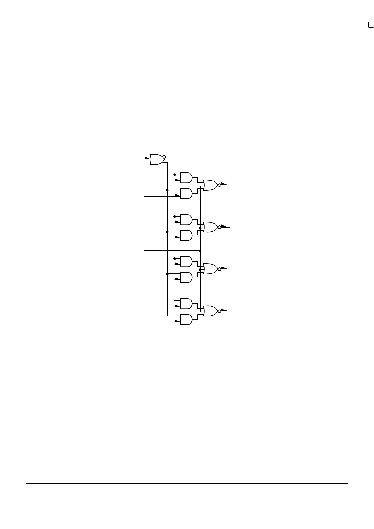
APPLICATION INFORMATION
The MC10H159 is a quad two channel multiplexer with
enable. It incorporates common enable and common
data select inputs. The select input determines which
data inputs are enabled. A high (H) level enables data
inputs D0 0, D1 0, D2 0, and D3 0. A low (L) level enables
data inputs D0 1, D1 1, D2 1, and D3 1. Any change on
the data inputs will be reflected at the outputs while the
enable is low. Input levels are inverted at the output.
LOGIC DIAGRAM
SELECT 9
D0 1 5
D0 0 6
D1 1 3
D1 0 4
D2 1 12
D2 0 13
D3 1 10
D3 0 11
1 Q0
2 Q1
15 Q2
14 Q3
ENABLE 7
VCC PIN 16
VEE PIN 8
 Loading...