

Motorola MC10H145FN, MC10H145L, MC10H145P Datasheet
SEMICONDUCTOR TECHNICAL DATA
2–233
REV 5
Motorola, Inc. 1996
3/93
The MC10H145 is a 16 x 4 bit register file. The active-low chip select allows
easy expansion.
The operating mode of the register file is controlled by the WE
input. When
WE
is “low” the device is in the write mode, the outputs are “low” and the data
present at Dn input is stored at the selected address, when WE
is “high,” the
device is in the read mode — the data state at the selected location is present
at the Qn outputs.
• Address Access Time, 4.5 ns Typical
• Power Dissipation, 700 mW Typical
• Improved Noise Margin 150 mV (Over Operating Voltage and
Temperature Range)
• Voltage Compensated
• MECL 10K-Compatible
MAXIMUM RATINGS
Characteristic Symbol Rating Unit
Power Supply (VCC = 0) V
EE
–8.0 to 0 Vdc
Input Voltage (VCC = 0) V
I
0 to V
EE
Vdc
Output Current— Continuous
— Surge
I
out
50
100
mA
Operating Temperature Range T
A
0 to +75 °C
Storage Temperature Range— Plastic
— Ceramic
T
stg
–55 to +150
–55 to +165
°C
ELECTRICAL CHARACTERISTICS (VEE = –5.2 V ±5%) (See Note)
0° 25° 75°
Ch
aracteristic
Symbol
Min Max Min Max Min Max
Unit
Power Supply Current I
E
— 160 — 163 — 165 mA
Input Current High I
inH
— 375 — 220 — 220 µA
Input Current Low I
inL
0.5 — 0.5 — 0.3 — µA
High Output Voltage V
OH
–1.02 –0.84 –0.98 –0.81 –0.92 –0.735 Vdc
Low Output Voltage V
OL
–1.95 –1.63 –1.95 –1.63 –1.95 –1.60 Vdc
High Input Voltage V
IH
–1.17 –0.84 –1.13 –0.81 –1.07 –0.735 Vdc
Low Input Voltage V
IL
–1.95 –1.48 –1.95 –1.48 –1.95 –1.45 Vdc
NOTE:
Each MECL 10H series circuit has been designed to meet the dc specifications shown in the test table,
after thermal equilibrium has been established. The circuit is in a test socket or mounted on a printed
circuit board and transverse air flow greater than 500 Ifpm is maintained. Outputs are terminated through
a 50-ohm resistor to –2.0 volts.
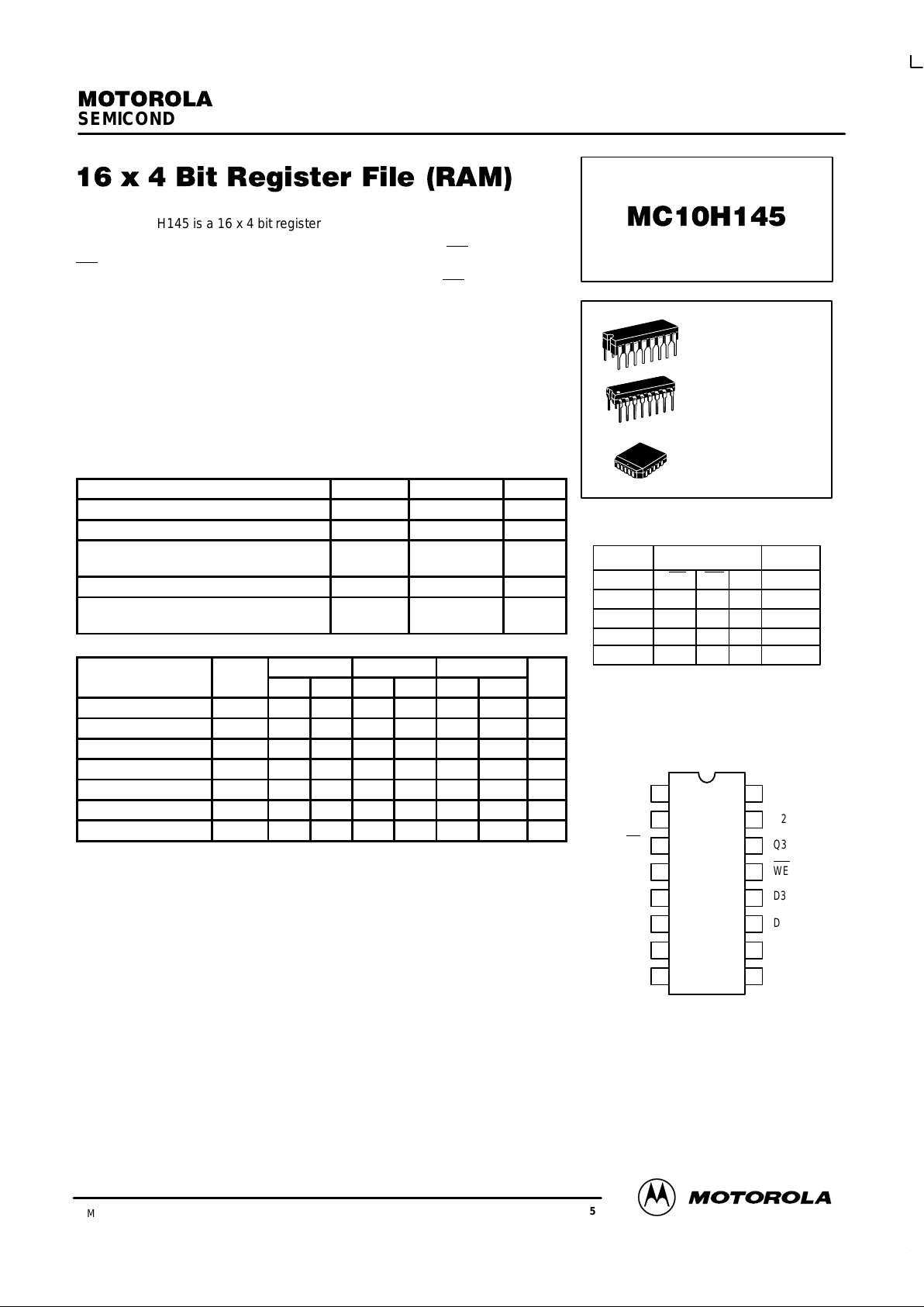
DIP
PIN ASSIGNMENT
Q1
Q0
CS
D1
D0
A3
A2
V
EE
V
CC
Q2
Q3
WE
D3
D2
A0
A1
16
15
14
13
12
11
10
9
1
2
3
4
5
6
7
8
TRUTH TABLE
MODE INPUT OUTPUT
CS
WE D
n
Write “0” L
X
Q
n
Write “1”
Read
Disabled
L
L
H
LLL
H
X
X
L
LH
L
Q
Q-State of Addressed Cell
L SUFFIX
CERAMIC PACKAGE
CASE 620–10
P SUFFIX
PLASTIC PACKAGE
CASE 648–08
FN SUFFIX
PLCC
CASE 775–02
Pin assignment is for Dual–in–Line Package.
For PLCC pin assignment, see the Pin Conversion
T ables on page 6–11 of the Motorola MECL Data
Book (DL122/D).
MC10H145
MOTOROLA MECL Data
DL122 — Rev 6
2–234
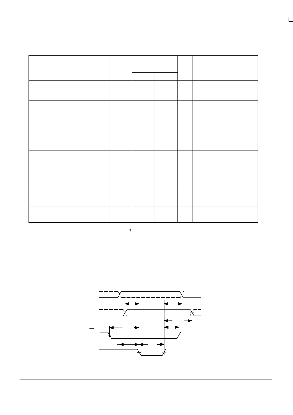
AC PARAMETERS
MC10H145
TA = 0 to +75°C,
VEE = –5.2 Vdc ±5%
Characteristics Symbol Min Max Unit Conditions
Read Mode
Chip Select Access Time
Chip Select Recovery Time
Address Access Time
t
ACS
t
RCS
t
AA
0
0
0
4.0
4.0
6.0
ns Measured from 50% of input to 50%
of output. See Note 2.
Write Mode
Write Pulse Width
Data Setup Time Prior to Write
Data Hold Time After Write
Address Setup Time Prior to Write
Address Hold Time After Write
Chip Select Setup Time Prior to Write
Chip Select Hold Time After Write
Write Disable Time
Write Recovery Time
t
W
t
WSD
t
WHD
t
WSA
t
WHA
t
WSCS
t
WHCS
t
WS
t
WR
6.0
0
1.5
3.5
1.5
0
1.5
1.0
1.0
—
—
—
—
—
—
—
4.0
4.0
ns t
WSA
= 3.5 ns
Measured at 50% of input to 50% of
output. tW = 6.0 ns.
Chip Enable Strobe Mode
Data Setup Prior to Chip Select
Write Enable Setup Prior to Chip Select
Address Setup Prior to Chip Select
Data Hold Time After Chip Select
Write Enable Hold Time After Chip Select
Address Hold Time After Chip Select
Chip Select Minimum Pulse Width
t
CSD
t
CSW
t
CSA
t
CHD
t
CHW
t
CHA
t
CS
0
0
0
1.0
0
2.0
4.0
—
—
—
—
—
—
—
ns Guaranteed but not tested on
standard product. See Figure 1.
Rise and Fall Time
Address to Output
CS to Output
tr, t
f
0.6
0.6
2.5
2.5
ns Measured between 20% and 80%
points.
Capacitance
Input Capacitance
Output Capacitance
C
in
C
out
—
—
6.0
8.0
pF Measured with a pulse technique.
NOTES: 1. T est circuit characteristics: RT = 50 Ω, MC10H145. CL p 5.0 pF (including jig and Stray Capacitance). Delay should be derated 30 ps/pF for
capacitive loads up to 50 pF.
2. The maximum Address Access Time is guaranteed to be the worst-case bit in the memory .
3. For proper use of MECL in a system environment, consult MECL System Design Handbook.
FIGURE 1 — CHIP ENABLE STROBE MODE
A
D
IN
WE
CS
T
CSA
T
CSW
T
CSD
T
CS
T
CHA
T
CHD
T
CHW
 Loading...