

MOTOROLA MC10H141FNR2, MC10H141LD Datasheet
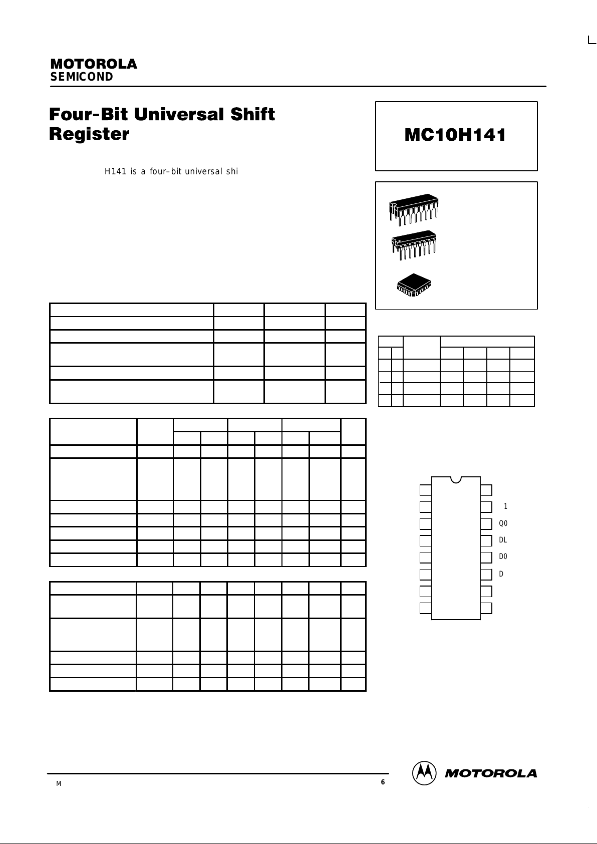
SEMICONDUCTOR TECHNICAL DATA
2–131
REV 6
Motorola, Inc. 1996
9/96
The MC10H141 is a four–bit universal shift register. This device is a
functional/pinout duplication of the standard MECL 10K part with 100%
improvement in propagation delay and operation frequency and no increase in
power supply current.
• Shift frequency, 250 MHz Min
• Power Dissipation, 425 mW Typical
• Improved Noise Margin 150 mV (over operating voltage and
temperature range)
• Voltage Compensated
• MECL 10K–Compatible
MAXIMUM RATINGS
Characteristic Symbol Rating Unit
Power Supply (VCC = 0) V
EE
–8.0 to 0 Vdc
Input Voltage (VCC = 0) V
I
0 to V
EE
Vdc
Output Current— Continuous
— Surge
I
out
50
100
mA
Operating Temperature Range T
A
0 to +75 °C
Storage Temperature Range— Plastic
— Ceramic
T
stg
–55 to +150
–55 to +165
°C
°C
ELECTRICAL CHARACTERISTICS (VEE = –5.2 V ±5%)
0° 25° 75°
Characteristic Symbol Min Max Min Max Min Max Unit
Power Supply Current I
E
— 112 — 102 — 112 mA
Input Current High
Pins 5,6,9,11,12,13
Pins 7,10
Pin 4
I
inH
—
—
—
405
416
510
—
—
—
255
260
320
—
—
—
255
260
320
µA
Input Current Low I
inL
0.5 — 0.5 — 0.3 — µA
High Output Voltage V
OH
–1.02 –0.84 –0.98 –0.81 –0.92 –0.735 Vdc
Low Output Voltage V
OL
–1.95 –1.63 –1.95 –1.63 –1.95 –1.60 Vdc
High Input Voltage V
IH
–1.17 –0.84 –1.13 –0.81 –1.07 –0.735 Vdc
Low Input Voltage V
IL
–1.95 –1.48 –1.95 –1.48 –1.95 –1.45 Vdc
AC PARAMETERS
Propagation Delay t
pd
1.0 2.0 1.0 2.0 1.1 2.1 ns
Hold Time —
Data, Select
t
hold
1.0 — 1.0 — 1.0 — ns
Set–up Time
Data
Select
t
set
1.5
3.0——
1.5
3.0——
1.5
3.0——
ns
Rise Time t
r
0.5 2.4 0.5 2.4 0.5 2.4 ns
Fall Time t
f
0.5 2.4 0.5 2.4 0.5 2.4 ns
Shift Frequency f
shift
250 — 250 — 250 — MHz
NOTE:
Each MECL 10H series circuit has been designed to meet the dc specifications shown in the test table,
after thermal equilibrium has been established. The circuit is in a test socket or mounted on a printed circuit
board and transverse air flow greater than 500 Iinear fpm is maintained. Outputs are terminated through
a 50 ohm resistor to –2.0 volts.
L
HQ2
n
32
n
H
Parallel Entry
Stop Shift Q0
n
DIP
PIN ASSIGNMENT
V
CC1
Q2
Q3
C
DR
D3
S2
V
EE
V
CC2
Q1
Q0
DL
D0
D1
S1
D2
16
15
14
13
12
11
10
9
1
2
3
4
5
6
7
8
TRUTH TABLE
SELECT
OPERATING
MODE
OUTPUTS
S1
S2 Q1n + 1Q2n + 1Q3n +
1
L
L
* Outputs as exist after pulse appears at “C” input with
input conditions as shown (Pulse Positive transition of
clock input).
D0 D1 D2 D3
H Shift Right* Q1nQ2nQ3nDR
H L Shift Left* DL Q0nQ1nQ2
n
Q1
n
Q0n +
1
L SUFFIX
CERAMIC PACKAGE
CASE 620–10
P SUFFIX
PLASTIC PACKAGE
CASE 648–08
FN SUFFIX
PLCC
CASE 775–02
Pin assignment is for Dual–in–Line Package.
For PLCC pin assignment, see the Pin Conversion
T ables on page 6–11 of the Motorola MECL Data
Book (DL122/D).
MC10H141
MOTOROLA MECL Data
DL122 — Rev 6
2–132
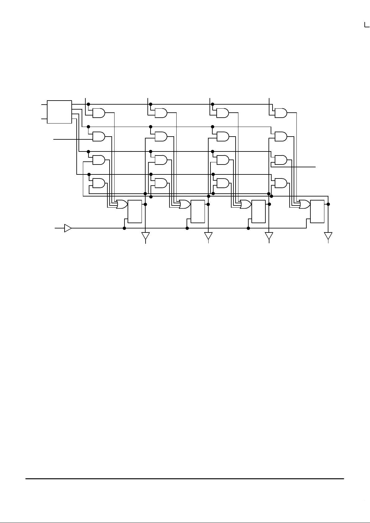
LOGIC DIAGRAM
PARALLEL ENTER
SHIFT RIGHT
SHIFT LEFT
HOLD
DQ
C
1 OF 4
DECODER
D3
DL
S1
DR
C
Q3
V
CC1 = PIN 1
S
CC2 = PIN 16
V
EE = PIN 8
S2
D2 D1 D0
Q2 Q1 Q0
DQ
C
DQ
C
DQ
C
APPLICATION INFORMATION
The MC10H141 is a four–bit universal shift
register which performs shift left, or shift right,
serial/parallel in, and serial/parallel out operations
with no external gating. Inputs S1 and S2 control the
four possible operations of the register without
external gating of the clock. The flip–flops shift
information on the positive edge of the clock. The
four operations are stop shift, shift left, shift right, and
parallel entry of data. The other six inputs are all data
type inputs; four for parallel entry data, and one for
shifting in from the left (DL) and one for shifting in
from the right (DR).
 Loading...