

Motorola MC10H135L, MC10H135P Datasheet
SEMICONDUCTOR TECHNICAL DATA
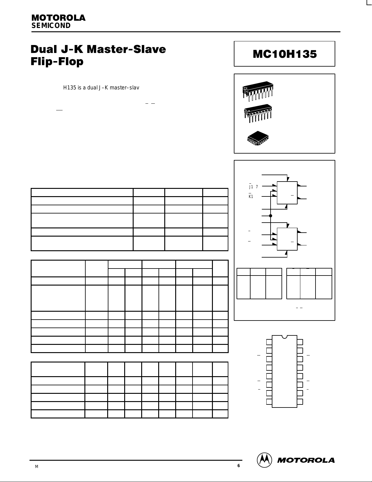
The MC10H135 is a dual J–K master–slave flip–flop. The device is provided
with an asynchronous set(s) and reset(R). These set and reset inputs overide
the clock.
A common clock is provided with separate J
static, the JK
inputs do not effect the output. The output states of the flip flop
change on the positive transition of the clock.
• Propagation delay, 1.5 ns Typical • Improved Noise Margin 150
• Power Dissipation, 280 mW mV (Over Operating Voltage
Typical/Pkg. (No Load) and Temperature Range)
• f
250 MHz Max• Voltage Compensated
tog
MAXIMUM RATINGS
Characteristic Symbol Rating Unit
Power Supply (VCC = 0) V
Input Voltage (VCC = 0) V
Output Current— Continuous
— Surge
Operating Temperature Range T
Storage Temperature Range— Plastic
— Ceramic
ELECTRICAL CHARACTERISTICS (VEE = –5.2 V ±5%) (See Note)
0° 25° 75°
Characteristic Symbol Min Max Min Max Min Max Unit
Power Supply Current I
Input Current High
Pins 6, 7, 10, 11
Pins 4, 5, 12, 13
Pin 9
Input Current Low Ii
High Output Voltage V
Low Output Voltage V
High Input Voltage V
Low Input Voltage V
I
E
inH
nL
OH
OL
IH
— 75 — 68 — 75 mA
—
460
—
800
—
675
0.5 — 0.5 — 0.3 — µA
–1.02 –0.84 –0.98 –0.81 –0.92 –0.735 Vdc
–1.95 –1.63 –1.95 –1.63 –1.95 –1.60 Vdc
–1.17 –0.84 –1.13 –0.81 –1.07 –0.735 Vdc
–1.95 –1.48 –1.95 –1.48 –1.95 –1.45 Vdc
IL
AC PARAMETERS
Propagation Delay
Set, Reset, Clock
Rise Time t
Fall Time t
Set–up Time t
Hold Time t
Toggle Frequency f
NOTE:
Each MECL 10H series circuit has been designed to meet the dc specifications shown in the test table,
after thermal equilibrium has been established. The circuit is in a test socket or mounted on a printed circuit
board and transverse air flow greater than 500 Ifpm is maintained. Outputs are terminated through a
50–ohm resistor to –2.0 volts.
t
pd
r
f
set
hold
tog
0.7 2.6 0.7 2.6 0.7 2.6 ns
0.7 2.2 0.7 2.2 0.7 2.2 ns
0.7 2.2 0.7 2.2 0.7 2.2 ns
1.5 — 1.5 — 1.5 — ns
1.0 — 1.0 — 1.0 — ns
250 — 250 — 250 — MHz
–K inputs. When the clock is
• MECL 10K–Compatible
–8.0 to 0 Vdc
0 to V
EE
50
100
0 to +75 °C
–55 to +150
–55 to +165
285
500
420
—
—
—
T
I
EE
I
out
A
stg
—
—
—
Vdc
mA
°C
°C
285
500
420
µA
L SUFFIX
CERAMIC PACKAGE
CASE 620–10
P SUFFIX
PLASTIC PACKAGE
CASE 648–08
FN SUFFIX
PLCC
CASE 775–02
LOGIC DIAGRAM
S1 5
1 7
J
1 6
K
R1 4
C 9
S2 12
J2 10
2 11
K
R2 13
RS TRUTH TABLE
RSQ
L
L
L
H
L
H
H
H
N.D. = Not Defined
n
Q
N.D.
Q1
Q1
Q2
Q
CLOCK J–K TRUTH TABLE*
J K Qn +
+
1
L
n
H
L
HLL
L
H
*Output states change on
positive transition of clock
for J
present.
DIP PIN ASSIGNMENT
1
V
CC1
Q1
Q
1
R1
S1
K
1
J
1
V
EE
Pin assignment is for Dual–in–Line Package.
For PLCC pin assignment, see the Pin Conversion
T ables on page 6–11 of the Motorola MECL Data
Book (DL122/D).
16
2
15
3
14
4
13
5
12
6
11
7
10
8
9
2
3
V
= PIN 1
CC1
V
= PIN 16
CC2
VEE= PIN 8
15
14
2
H
H
–K input condition
V
CC2
Q2
Q2
R2
S2
K2
J2
C
Q
n
L
H
Q
n
1
9/96
Motorola, Inc. 1996
2–89
REV 6
MC10H135
OUTLINE DIMENSIONS
FN SUFFIX
PLASTIC PLCC PACKAGE
CASE 775–02
ISSUE C
–L–
20 1
Z
C
G
G1
0.010 (0.250) N
S
T
–N–
L–M
S
Y BRK
–M–
W
V
A
0.007 (0.180) N
0.007 (0.180) N
R
E
0.004 (0.100)
J
PLANE
SEATING
–T–
VIEW S
S
0.007 (0.180) N
B
0.007 (0.180) N
U
M
S
L–M
T
M
S
S
L–M
T
S
D
Z
D
X
0.010 (0.250) N
G1
S
S
L–M
T
S
VIEW D–D
M
M
S
L–M
T
L–M
T
S
S
S
0.007 (0.180) N
H
M
S
L–M
T
S
K1
K
0.007 (0.180) N
F
M
S
L–M
T
S
VIEW S
NOTES:
1. DATUMS –L–, –M–, AND –N– DETERMINED
WHERE TOP OF LEAD SHOULDER EXITS PLASTIC
BODY AT MOLD PARTING LINE.
2. DIMENSION G1, TRUE POSITION TO BE
MEASURED AT DA TUM –T–, SEATING PLANE.
3. DIMENSIONS R AND U DO NOT INCLUDE MOLD
FLASH. ALLOWABLE MOLD FLASH IS 0.010 (0.250)
PER SIDE.
4. DIMENSIONING AND TOLERANCING PER ANSI
Y14.5M, 1982.
5. CONTROLLING DIMENSION: INCH.
6. THE PACKAGE TOP MAY BE SMALLER THAN THE
PACKAGE BOTTOM BY UP TO 0.012 (0.300).
DIMENSIONS R AND U ARE DETERMINED AT THE
OUTERMOST EXTREMES OF THE PLASTIC BODY
EXCLUSIVE OF MOLD FLASH, TIE BAR BURRS,
GATE BURRS AND INTERLEAD FLASH, BUT
INCLUDING ANY MISMATCH BETWEEN THE TOP
AND BOTTOM OF THE PLASTIC BODY.
7. DIMENSION H DOES NOT INCLUDE DAMBAR
PROTRUSION OR INTRUSION. THE DAMBAR
PROTRUSION(S) SHALL NOT CAUSE THE H
DIMENSION TO BE GREATER THAN 0.037 (0.940).
THE DAMBAR INTRUSION(S) SHALL NOT CAUSE
THE H DIMENSION TO BE SMALLER THAN 0.025
(0.635).
MOTOROLA MECL Data
DIM MIN MAX MIN MAX
A 0.385 0.395 9.78 10.03
B 0.385 0.395 9.78 10.03
C 0.165 0.180 4.20 4.57
E 0.090 0.110 2.29 2.79
F 0.013 0.019 0.33 0.48
G 0.050 BSC 1.27 BSC
H 0.026 0.032 0.66 0.81
J 0.020 ––– 0.51 –––
K 0.025 ––– 0.64 –––
R 0.350 0.356 8.89 9.04
U 0.350 0.356 8.89 9.04
V 0.042 0.048 1.07 1.21
W 0.042 0.048 1.07 1.21
X 0.042 0.056 1.07 1.42
Y ––– 0.020 ––– 0.50
Z 2 10 2 10
____
G1 0.310 0.330 7.88 8.38
K1 0.040 ––– 1.02 –––
2–90
MILLIMETERSINCHES
DL122 — Rev 6
 Loading...