

Motorola MC10H130FN, MC10H130L, MC10H130P Datasheet
SEMICONDUCTOR TECHNICAL DATA
The MC10H130 is a MECL 10H part which is a functional/pinout duplication
of the standard MECL 10K family part, with 100% improvement in clock speed
and propagation delay and no increase in power–supply current.
• Propagation Delay, 1.0 ns Typical
• Power Dissipation, 155 mW Typical
• Improved Noise Margin 150 mV (Over Operating Voltage and
Temperature Range)
• Voltage Compensated
• MECL 10K–Compatible
MAXIMUM RATINGS
Characteristic Symbol Rating Unit
Power Supply (VCC = 0) V
Input Voltage (VCC = 0) V
Output Current— Continuous
— Surge
Operating Temperature Range T
Storage Temperature Range— Plastic
— Ceramic
T
I
EE
I
out
A
stg
ELECTRICAL CHARACTERISTICS (VEE = –5.2 V ±5%) (See Note)
0° 25° 75°
Characteristic Symbol Min Max Min Max Min Max Unit
Power Supply Current I
Input Current High
Pins 6, 11
Pins 7, 9, 10
Pins 4, 5, 12, 13
Input Current Low I
High Output Voltage V
Low Output Voltage V
High Input Voltage V
Low Input Voltage V
I
E
inH
inL
OH
OL
IH
— 38 — 35 — 38 mA
—
468
545
434
—
—
—
—
—
0.5 — 0.5 — 0.3 — µA
–1.02 –0.84 –0.98 –0.81 –0.92 –0.735 Vdc
–1.95 –1.63 –1.95 –1.63 –1.95 –1.60 Vdc
–1.17 –0.84 –1.13 –0.81 –1.07 –0.735 Vdc
–1.95 –1.48 –1.95 –1.48 –1.95 –1.45 Vdc
IL
AC PARAMETERS
Propagation Delay
Data
Set, Reset
Clock, CE
Rise Time t
Fall Time t
Set–up Time t
Hold Time t
NOTE:
Each MECL 10H series circuit has been designed to meet the dc specifications shown in the test table,
after thermal equilibrium has been established. The circuit is in a test socket or mounted on a printed circuit
board and transverse air flow greater than 500 Iinear fpm is maintained. Outputs are terminated through
a 50–ohm resistor to –2.0 volts.
t
pd
r
f
set
hold
0.4
1.6
1.7
1.6
0.4
0.7
0.5
0.6
0.5
0.5 1.6 0.5 1.7 0.5 1.8 ns
0.5 1.6 0.5 1.7 0.5 1.8 ns
2.2 — 2.2 — 2.2 — ns
0.7 — 0.7 — 0.7 — ns
–8.0 to 0 Vdc
0 to V
EE
50
100
0 to +75 °C
–55 to +150
–55 to +165
275
320
255
1.7
1.8
1.7
—
—
—
0.4
0.8
0.6
Vdc
mA
°C
°C
275
320
255
1.8
1.9
1.8
µA
ns
CERAMIC PACKAGE
PLASTIC PACKAGE
S1 5
D1 7
CE
R1 4
C
R2 13
CE
D2 10
S2 12
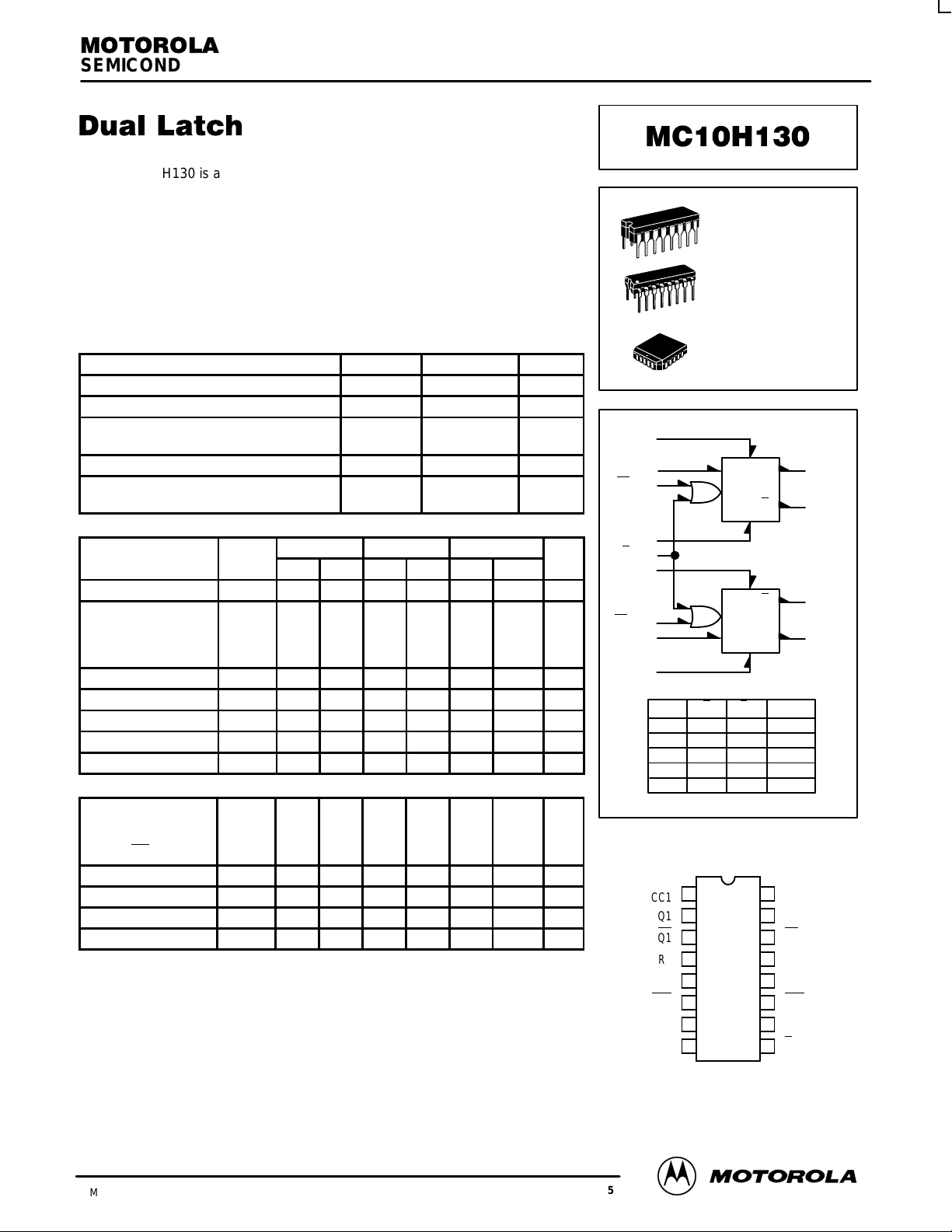
LOGIC DIAGRAM
1 6
9
2 11
TRUTH TABLE
DCCEQ
L
L
L
H
L
X
H
X
H
X
DIP
PIN ASSIGNMENT
Q1
Q1
R1
S1
E1
D1
EE
1
2
3
4
5
6
7
8
V
CC1
C
V
L SUFFIX
CASE 620–10
P SUFFIX
CASE 648–08
FN SUFFIX
PLCC
CASE 775–02
Q1
1
Q
V
= PIN 1
CC1
V
= PIN 16
CC2
VEE = PIN 8
Q
2
Q2
n+1
L
L
L
H
H
Q
L
H
16
15
14
13
12
11
10
n
Q
n
Q
n
V
CC2
Q2
Q2
R2
S2
C
E2
D2
9
C
2
3
14
15
3/93
Motorola, Inc. 1996
2–49
Pin assignment is for Dual–in–Line Package.
For PLCC pin assignment, see the Pin Conversion
T ables on page 6–11 of the Motorola MECL Data
Book (DL122/D).
REV 5

MC10H130
APPLICATION INFORMATION
The MC10H130 is a clocked dual D type latch. Each
latch may be clocked separately by holding the common
clock in the low state, and using the clock enable inputs
for the clocking function. If the common clock is to be used
to clock the latch, the clock enable (CE)
in the low state. In this mode, the enable inputs perform
the function of controlling the common clock (C)
Any change at the D input will be reflected at the output
inputs must be
.
while the clock is low. The outputs are latched on the
positive transition of the clock. While the clock is in the
high state, a change in the information present at the data
inputs will not affect the output information.
The set and reset inputs do not override the clock and
D inputs. They are effective only when either C
both are high.
or CE or
MOTOROLA MECL Data
2–50
DL122 — Rev 6
 Loading...