

Motorola MC10H016FN, MC10H016FNR2, MC10H016L, MC10H016P Datasheet
SEMICONDUCTOR TECHNICAL DATA
The MC10H016 is a high–speed synchronous, presettable, cascadable
4–bit binary counter. It is useful for a large number of conversion, counting and
digital integration applications.
• Counting Frequency , 200 MHz Minimum
• Improved Noise Margin 150 mV (Over Operating Voltage and
Temperature Range)
• Voltage Compensated
• MECL 10K–Compatible
• Positive Edge Triggered
MAXIMUM RATINGS
Characteristic Symbol Rating Unit
Power Supply (VCC = 0) V
Input Voltage (VCC = 0) V
Output Current — Continuous
— Surge
Operating T emperature Range T
Storage T emperature Range — Plastic
— Ceramic
EE
I
I
out
A
T
stg
–8.0 to 0 Vdc
0 to V
EE
50
100
0 to +75 °C
–55 to +150
–55 to +165
Vdc
mA
°C
ELECTRICAL CHARACTERISTICS (VEE = –5.2 V ±5%) (See Note)
0° 25° 75°
Characteristic Symbol Min Max Min Max Min Max Unit
Power Supply Current I
Input Current High
All Except MR
Pin 12 MR
Input Current Low I
High Output Voltage V
Low Output Voltage V
High Input Voltage V
Low Input Voltage V
I
E
inH
inL
OH
OL
IH
— 126 — 115 — 126 mA
——450
1190——
0.5 — 0.5 — 0.3 — µA
–1.02 –0.84 –0.98 –0.81 –0.92 –0.735 Vdc
–1.95 –1.63 –1.95 –1.63 –1.95 –1.60 Vdc
–1.17 –0.84 –1.13 –0.81 –1.07 –0.735 Vdc
–1.95 –1.48 –1.95 –1.48 –1.95 –1.45 Vdc
IL
265
700——
265
700
AC PARAMETERS
Propagation Delay
Clock to Q
Clock to TC
MR to Q
Set–up Time
Pn to Clock
CE
or PE to Clock
Hold Time
Clock to P
Clock to CE
Counting Frequency f
Rise Time t
Fall Time t
NOTE:
Each MECL 10H series circuit has been designed to meet the dc specifications shown in the test table,
after thermal equilibrium has been established. The circuit is in a test socket or mounted on a printed circuit
board and transverse air flow greater than 500 Ifpm is maintained. Outputs are terminated through a
50–ohm resistor to –2.0 volts.
n
or PE
t
pd
t
set
t
hold
count
r
f
1.0
2.4
1.0
2.5
1.0
0.7
2.4
0.7
0.7
2.4
2.0
2.5——
1.0
0.5——
200 — 200 — 200 — MHz
0.5 2.0 0.5 2.1 0.5 2.2 ns
0.5 2.0 0.5 2.1 0.5 2.2 ns
2.5
0.7
2.5
2.0
2.5——
1.0
0.5——
0.7
0.7
2.0
2.5
1.0
0.5
2.7
2.6
2.6
—
—
—
—
µA
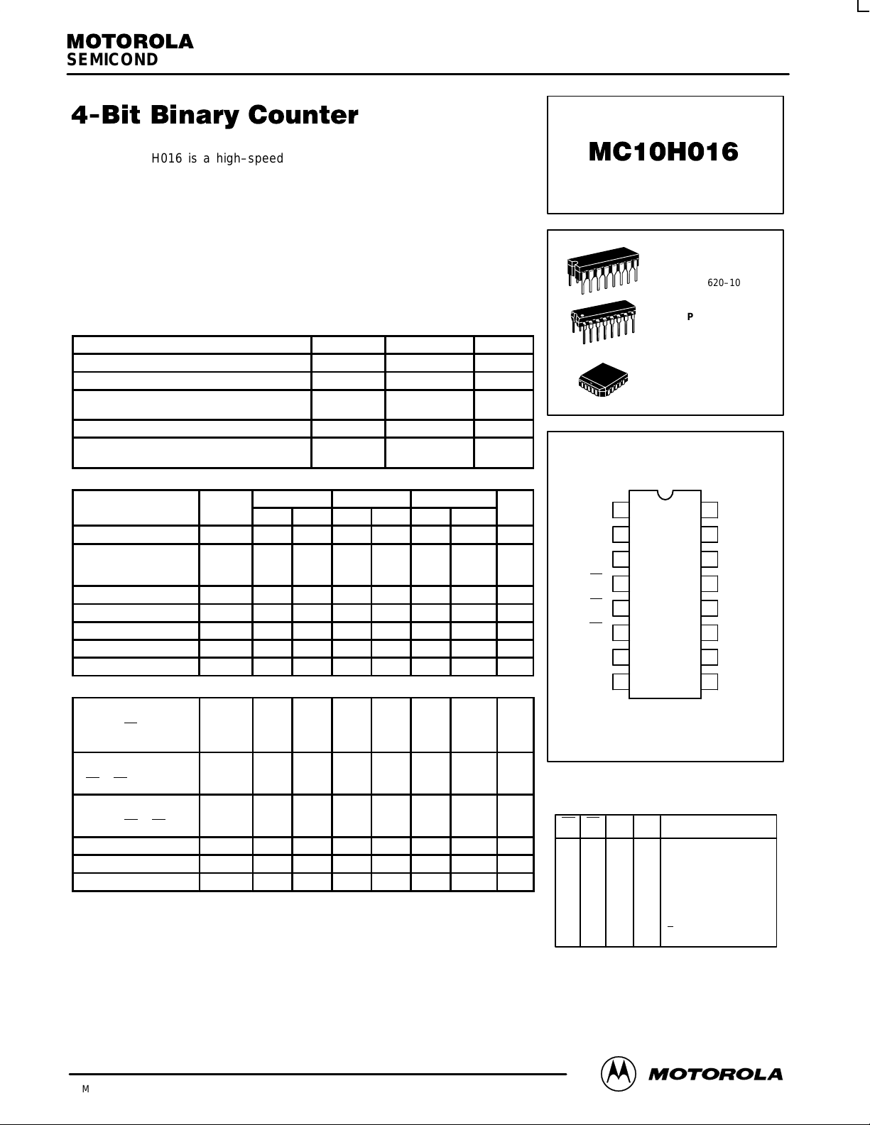
L SUFFIX
CERAMIC PACKAGE
CASE 620–10
P SUFFIX
PLASTIC PACKAGE
CASE 648–08
FN SUFFIX
PLCC
CASE 775–02
DIP
PIN ASSIGNMENT
V
CC1
Q1
Q0
TC
PE
CE
PO
V
EE
ns
ns
ns
Pin assignment is for Dual–in–Line Package.
For PLCC pin assignment, see the Pin Conversion
T ables on page 6–11 of the Motorola MECL Data
CE PE MR CP Function
L
L
L
H
H
L
H
H
X
X
X
X
Z = Clock Pulse (Low to High);ZZ = Clock Pulse (High to Low)
1
2
3
4
5
6
7
16
15
14
13
12
11
10
8
Book (DL122/D).
TRUTH TABLE
Load Parallel (Pn to Qn)
Z
L
L
L
L
L
H
Load Parallel (Pn to Qn)
Z
Count
Z
Hold
Z
Masters Respond;
ZZ
Slaves Hold
Reset (Qn = LOW,
X
T
= HIGH)
C
V
CC2
Q2
Q3
CP
MR
P3
P2
P1
9
9/96
Motorola, Inc. 1996
2–1
Features include assertion inputs and outputs on each
of the four master/slave counting flip–flops. Terminal
count is generated internally in a manner that allows
synchronous loading at nearly the speed of the basic
counter.
REV 6

MC10H016
TC
Q
FO
MASTER SLAVE
MSB
MR
Tc
P0–P3
C
PECE
Q0–Q3
1/2 10H1091/2 10H1091/2 10H109
MR
MR
Tc
P0–P3
C
Tc
5
P0–P3
C
Q
Q
Q
Q
PECE
Q0–Q3
PECE
Q0–Q3
Q
Q
4–Bit Binary Counter Logic Diagram
MASTER SLAVE
P1 P2 P3
Q
Q
CE
MR
PE
Q0 Q1 Q2 Q3
Q
MASTER SLAVE
P0
CP
PECE
Q0–Q3
propagation delays as many gate functions are achieved internally without incurring a full gate delay.
Note that this diagram is provided for understanding of logic operation only. It should not be used for evaluation of
PECE
1/2 10H109
Q0–Q3
LSB
MR
MR
÷N Counter 1 to 16
Tc
MC10H016 Cascaded for 5 Stage Presettable Counter
Max freq. is only OR gate delay below max when counting alone.
P0–P3
C
Tc
P0–P3
C
CLOCK
MOTOROLA MECL Data
2–2
DL122 — Rev 6
 Loading...