

Motorola MC10162FN, MC10162L, MC10162P Datasheet
SEMICONDUCTOR TECHNICAL DATA
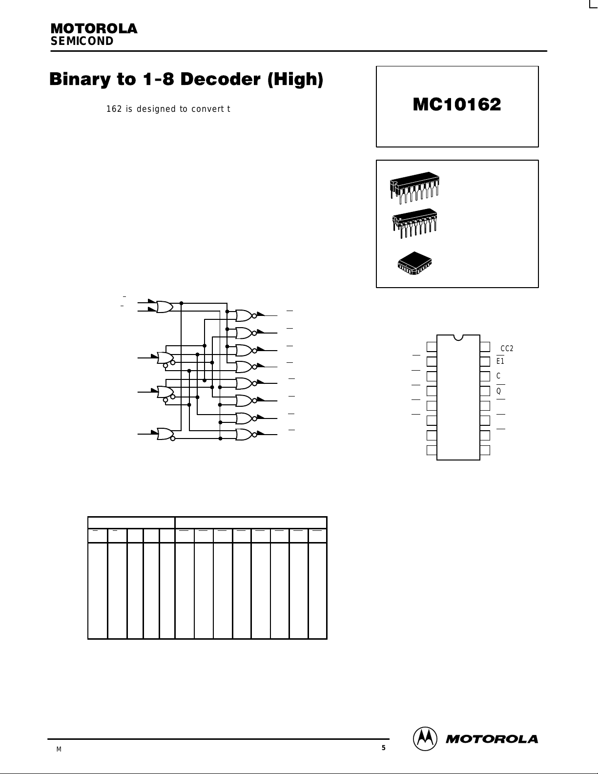
The MC10162 is designed to convert three lines of input data to a
one–of–eight output. The selected output will be high while all other outputs are
low. The enable inputs, when either or both are high, force all outputs low.
The MC10162 is a true parallel decoder. No series gating is used internally,
eliminating unequal delay times found in other decoders.
This device is ideally suited for demultiplexer applications. One of the two
enable inputs is used as the data input, while the other is used as a data enable
input.
A complete mux/demux operation on 16 bits for data distribution is illustrated
in Figure 1 of the MC10161 data sheet.
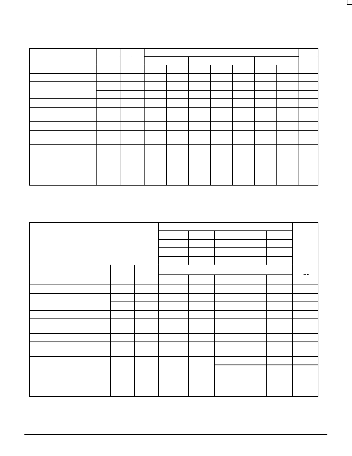
PD= 315 ns typ/pkg (No Load)
tpd= 4.0 ns typ
tr, tf= 2.0 ns typ (20%–80%)
LOGIC DIAGRAM
E02
E115
A7
B9
C14
TRUTH TABLE
INPUTS OUTPUTS
E0 E1 C B A Q0 Q1 Q2 Q3 Q4 Q5 Q6 Q7
L L L L L H L L L L L L L
L L L L H L H L L L L L L
L L L H L L L H L L L L L
L L L H H L L L H L L L L
L L H L L L L L L H L L L
L L H L H L L L L L H L L
L L H H L L L L L L L H L
L L H H H L L L L L L L H
H X X X X L L L L L L L L
X H X X X L L L L L L L L
6Q0
5Q1
4Q2
3Q3
13 Q4
12 Q5
11 Q6
10 Q7
V
= PIN 1
CC1
V
= PIN 16
CC2
VEE= PIN 8
L SUFFIX
CERAMIC PACKAGE
CASE 620–10
P SUFFIX
PLASTIC PACKAGE
CASE 648–08
FN SUFFIX
PLCC
CASE 775–02
DIP
PIN ASSIGNMENT
1
V
CC1
E0
Q3
Q2
Q1
Q0
A
V
EE
Pin assignment is for Dual–in–Line Package.
For PLCC pin assignment, see the Pin Conversion
T ables on page 6–11 of the Motorola MECL Data
Book (DL122/D).
16
V
CC2
2
15
E1
3
14
C
4
13
Q4
5
12
Q5
6
11
Q6
7
10
Q7
8
9
B
3/93
Motorola, Inc. 1996
3–78
REV 5
MC10162
Under
Und
(VCC)
ELECTRICAL CHARACTERISTICS
Test Limits
Pin
Characteristic Symbol
Power Supply Drain Current I
Input Current I
Output Voltage Logic 1 V
Output Voltage Logic 0 V
Threshold Voltage Logic 1 V
Threshold Voltage Logic 0 V
Switching Times (50Ω Load) ns
Propagation Delay t
Rise Time (20 to 80%) t
Fall Time (20 to 80%) t
E
inH
I
inL
OH
OL
OHA
OLA
14+13–
t
14–13+
13+
13–
Under
Test
8 84 61 76 84 mAdc
14 350 220 220 µAdc
14 0.5 0.5 0.3 µAdc
13 –1.060 –0.890 –0.960 –0.810 –0.890 –0.700 Vdc
13
13
13 –1.080 –0.980 –0.910 Vdc
13
13
13
13
13 1.0 3.3 1.1 2.0 3.3 1.1 3.5
13 1.0 3.3 1.1 2.0 3.3 1.1 3.5
–30°C +25°C +85°C
Min Max Min Typ Max Min Max
–1.890
–1.890
1.5
1.5
–1.675
–1.675
–1.655
–1.655
6.2
6.2
–1.850
–1.850
1.5
1.5
4.0
4.0
–1.650
–1.650
–1.630
–1.630
6.0
6.0
–1.825
–1.825
1.5
1.5
–1.615
–1.615
–1.595
–1.595
6.4
6.4
Unit
Vdc
Vdc
ELECTRICAL CHARACTERISTICS (continued)
TEST VOLTAGE VALUES (Volts)
@ Test Temperature V
–30°C –0.890 –1.890 –1.205 –1.500 –5.2
+25°C –0.810 –1.850 –1.105 –1.475 –5.2
+85°C –0.700 –1.825 –1.035 –1.440 –5.2
Pin
Characteristic Symbol
Power Supply Drain Current I
Input Current I
Output Voltage Logic 1 V
Output Voltage Logic 0 V
Threshold Voltage Logic 1 V
Threshold Voltage Logic 0 V
Switching Times (50Ω Load) Pulse In Pulse Out –3.2 V +2.0 V
Propagation Delay t
Rise Time (20 to 80%) t+ 13 14 13 8 1,16
Fall Time (20 to 80%) t– 13 14 13 8 1,16
E
inH
I
inL
OH
OL
OHA
OLA
14+13+
t
14–13–
er
Test
8 8 1,16
14 14 8 1,16
14 14 8 1,16
13 14 8 1,16
13
13
13 14 8 1,16
13
13
13
13
IHmax
TEST VOLTAGE APPLIED TO PINS LISTED BELOW
V
IHmax
2
15
V
ILmin
V
ILmin
V
IHAminVILAmax
V
IHAminVILAmax
2
15
14
14
13
13
V
EE
V
EE
8
8
8
8
8
8
Gnd
1,16
1,16
1,16
1,16
1,16
1,16
Each MECL 10,000 series circuit has been designed to meet the dc specifications shown in the test table, after thermal equilibrium has been
established. The circuit is in a test socket or mounted on a printed circuit board and transverse air flow greater than 500 linear fpm is maintained.
Outputs are terminated through a 50–ohm resistor to –2.0 volts. Test procedures are shown for only one gate. The other gates are tested in the
same manner.
3–79 MOTOROLAMECL Data
DL122 — Rev 6
 Loading...