

Motorola MC10160L, MC10160P Datasheet
SEMICONDUCTOR TECHNICAL DATA
3–69
REV 6
Motorola, Inc. 1996
9/96
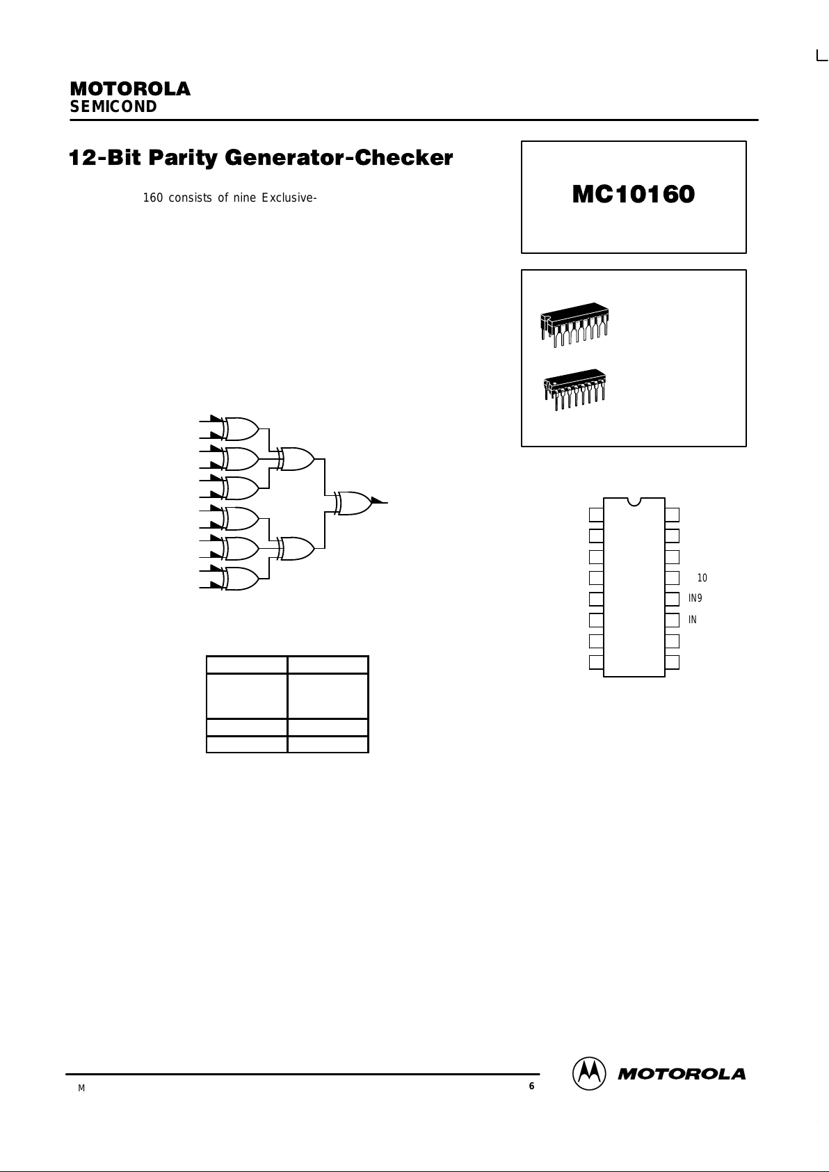
The MC10160 consists of nine Exclusive-OR gates in a single package,
internally connected to provide odd parity checking or generation. Output goes
high when an odd number of inputs are high. Unconnected inputs are pulled to
low logic levels allowing parity detection and generation for less than 12 bits.
PD= 320 mW typ/pkg (No Load)
tpd= 5.0 ns typ
tr, tf= 2.0 ns typ (20%–80%)
LOGIC DIAGRAM
V
CC1
= PIN 1
V
CC2
= PIN 16
VEE= PIN 8
15
14
13
12
11
10
9
7
6
5
4
3
2
INPUT OUTPUT
Sum of
High Level
Inputs
Pin 2
Even Low
Odd High
V
CC1
OUT
IN1
IN2
IN3
IN4
IN5
V
EE
V
CC2
IN12
IN11
IN10
IN9
IN8
IN7
IN6
16
15
14
13
12
11
10
9
1
2
3
4
5
6
7
8
PIN ASSIGNMENT
L SUFFIX
CERAMIC PACKAGE
CASE 620–10
P SUFFIX
PLASTIC PACKAGE
CASE 648–08
MC10160
MOTOROLA MECL Data
DL122 — Rev 6
3–70
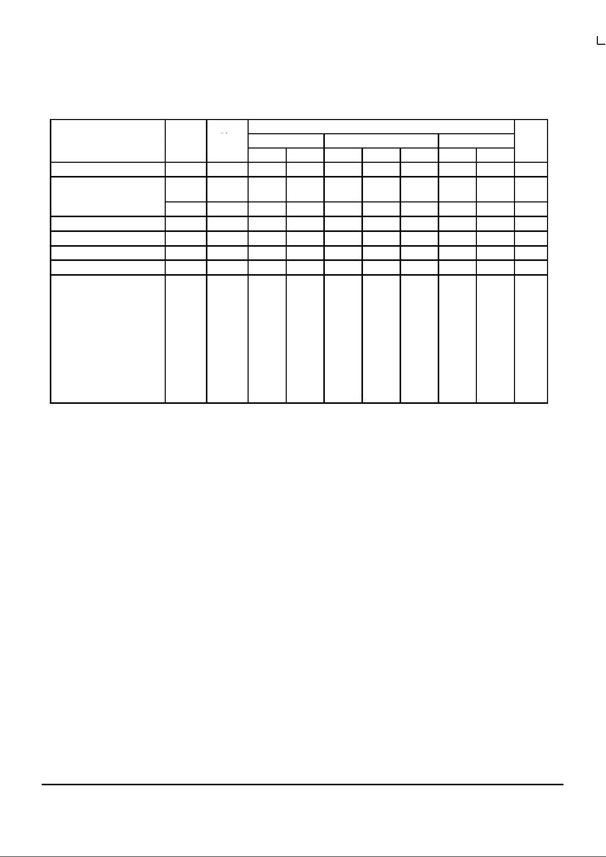
ELECTRICAL CHARACTERISTICS
Test Limits
Pin
Under
–30°C +25°C +85°C
Characteristic Symbol
Under
Test
Min Max Min Typ Max Min Max
Unit
Power Supply Drain Current I
E
8 86 62 78 86 mAdc
Input Current I
inH
(Note 1.)
3
4
425
350
265
220
265
220
µAdc
I
inL
3 0.5 0.5 0.3 µAdc
Output Voltage Logic 1 V
OH
2 –1.060 –0.890 –0.960 –0.810 –0.890 –0.700 Vdc
Output Voltage Logic 0 V
OL
2 –1.890 –1.675 –1.850 –1.650 –1.825 –1.615 Vdc
Threshold Voltage Logic 1 V
OHA
2 –1.080 –0.980 –0.910 Vdc
Threshold Voltage Logic 0 V
OLA
2 –1.655 –1.630 –1.595 Vdc
Switching Times (50Ω Load) ns
Propagation Delay t
3+2+
t
3+2–
t
3–2–
t
3–2+
t
4+2+
t
4+2–
t
4–2–
t
4–2+
2
2
2
2
2
2
2
2
1.8
1.8
1.8
1.8
1.8
1.8
1.8
1.8
8.1
8.1
8.1
8.1
8.1
8.1
8.1
8.1
2.0
2.0
2.0
2.0
2.0
2.0
2.0
2.0
5.0
5.0
5.0
5.0
5.0
5.0
5.0
5.0
7.5
7.5
7.5
7.5
7.5
7.5
7.5
7.5
2.0
2.0
2.0
2.0
2.0
2.0
2.0
2.0
8.0
8.0
8.0
8.0
8.0
8.0
8.0
8.0
Rise Time (20 to 80%) t
2+
2 1.1 3.5 1.1 2.0 3.3 1.0 3.5
Fall Time (20 to 80%) t
2–
2 1.1 3.5 1.1 2.0 3.3 1.0 3.5
1. Pins 3, 6, 7, 11, 12, 15 are similar. Pins 4, 5, 9, 10, 13, 14 are similar.
 Loading...