

Page 1

M68ICS08ABUM/D
M68ICS08AB
IN-CIRCUIT SIMULATOR
Februrary 2000
HARDWARE
USER’S MANUAL
© MOTOROLA, Inc., 1998-1999; All Rights Reserved
Page 2

Important Notice to Users
While every effort has been made to ensure the accuracy of all information in this document, Motorola
assumes no liability to any party for any loss or damage caused by errors or omissions or by statements of
any kindin thisdocument,itsupdates, supplements, or special editions,whethersucherrorsareomissions or
statements result from negligence, accident, or any other cause. Motorola further assumes no liability arising
out of the application or use of any information, product, or system described herein; nor any liability for
incidental or consequential damages arising from the use of this document. Motorola disclaims all
warranties regarding the information contained herein, whether expressed, implied, or statutory, including
implied warranties of merchantability or fitness for a particular purpose. Motorola makes no representation
that the interconnection of products in the manner described herein will not infringe on existing or future
patent rights, nor do the descriptions contained herein imply the granting or license to make, use, or sell
equipment constructed in accordance with this description.
Motorola reserves the right to make changes without further notice to any products herein. Motorola makes
no warranty, representation or guarantee regarding the suitability of its products for any particular purpose,
nor does Motorola assume any liability arising out of the application or use of any product or circuit, and
specifically disclaims any and all liability, including, without limitation, consequential or incidental
damages. “Typical” parameters can and do vary in different applications. All operating parameters,
including “typicals” must be validated for each customer application by customer’s technical experts.
Motorola does not convey any license under its patent rights nor the rights of others. Motorola products are
not designed, intended,or authorizedforuseascomponentsinsystemsintended for surgical implant into the
body, or other applications intended to support or sustain life, or for any other application in which the
failure of the Motorola product could create a situation where personal injury or death may occur. Should
Buyer purchase or use Motorola products for any such unintended or unauthorized application, Buyer shall
indemnify and hold Motorola and its officers, employees, subsidiaries, affiliates, and distributors harmless
against all claims, costs, damages, and expenses, and reasonable attorney fees arising out of, directly or
indirectly, any claim of personal injuryor death associated with such unintended or unauthorized use, even if
such claim alleges that Motorola was negligent regarding the design or manufacture of the part.
Trademarks
This document includes these trademarks:
Motorola and the Motorola logo are registered trademarks of Motorola, Inc.
IBM is a registered trademark of International Business Machines Corporation.
Windows is a registered trademark of Microsoft Corporation.
CASM08W, ICS08RKW, PROG08SW, ICD08SW, and WinIDE software are ã P & E Microcomputer
Systems, Inc., 1996; all rights reserved.
Motorola, Inc. is an Equal Opportunity/Affirmative Action Employer.
Page 3

1-1 INTRODUCTION 1-1
OVERVIEW 1-1
ABICS Product Components 1-2
M68ICS08AB HARDWARE 1-2
Specifications 1-3
ABICS INTERFACE MODULE OVERVIEW 1-4
Board Interface Connectors 1-5
MCU Subsystem 1-6
TARGET CABLES 1-11
FLEX Cable 1-11
MON08 Cable 1-12
ABOUT THIS OPERATOR’S MANUAL 1-12
Chapter Organization 1-12
Document Conventions 1-13
HARDWARE QUICK START INSTRUCTIONS 1-14
CUSTOMER SUPPORT 1-14
2-1 HARDWARE INSTALLATION 2-1
OVERVIEW 2-1
CONFIGURING THE IN-CIRCUIT SIMULATOR BOARD 2-2
INSTALLING THE HARDWARE 2-3
CONNECTING TO A TARGET SYSTEM 2-3
3-1 USING THE MON08 INTERFA CE 3-1
OVERVIEW 3-1
HEADER PLACEMENT AND LAYOUT 3-1
CONNECTING TO THE IN-CIRCUIT SIMULATOR 3-3
DISABLING THE TARGET-SYSTEM INTERFACE 3-4
A-1 TECHNICAL REFERENCE & TROUBLESHOOTING A-1
OVERVIEW A-1
CPU32XIPB/D -1
Page 4

FUNCTIONAL DESCRIPTION A-2
ICS08AB32 Board A-2
TROUBLESHOOTING THE QUICK START A-4
TROUBLESHOOTING MON08 MODE A-7
CONNECTOR PIN ASSIGNMENTS A-11
TARGET-CABLE PIN ASSIGNMENTS A-17
PARTS LIST A-21
BOARD LAYOUT AND SCHEMATIC DIAGRAMS A-23
B-1 GLOSSARY B-1
-2 CPU32XIPB/D
Page 5

1-1. ABICS Board Layout ................................................................................................. 1-4
1-2. ICS Functional Overview ........................................................................................... 1-5
1-3. MC68HC908AB32 In-Circuit Simulator Block Diagram .......................................... 1-6
1-4. FLEX Cable .............................................................................................................. 1-12
3-1. MON08 Target System Connector Layout ................................................................. 3-3
3-2. Target System Stand-Alone Connection .................................................................... 3-4
A-1. IC508AB32 Board Layout ....................................................................................... A-24
CPU32XIPB/D -3
Page 6

-4 CPU32XIPB/D
Page 7

M68ICS08AB Product Components 1-2
M68ICS08AB Specifications 1-3
Target Interface 1-10
FLEX Cable Connectors 1-11
MON08 Cable Connectors 1-12
P9 Configuration Header – DTR switch on-board regulator 2-2
P4 Configuration Header – Target Cable Reset Pin Function 2-2
P6 Configuration Header – Oscillator Source 2-3
MON08 Target System Connector P1 3-2
MON08 Target System Connector P2 3-3
Target Connector P7 A-11
Target Connector P8 A-13
MON08 Connector J2 A-15
FLEX Target Cable (M68CBL05C)
for QFP Target Head Adapters A-17
Target MON08 Cable A-21
ICS08AB32 Parts List A-21
CPU32XIPB/D -5
Page 8

-6 CPU32XIPB/D
Page 9

1.1 OVERVIEW
This chapter provides an overview of the Motorola M68ICS08AB in-circuit
simulator (ABICS) and a quick start guide to setting up a development project.
The ABICS board, a 107 ´ 109-mm PCB (printed circuit board), is a standalone development and debugging aid for designers using MC68HC908AB32
microcontroller unit (MCU) devices. The ABICS contains both the hardware
(the M68ICS08AB) and software (ICD08SZã) needed to develop and simulate
source code for, and to program, Motorola’s MC68HC908AB32
microcontrollers. Refer to the M68ICS08AB IN-CIRCUIT SIMULATOR
SOFTW ARE OPERATOR’S MANUAL for detailed information about the
ICD08SZ software.
The ABICS and the ICS08AB software form a complete simulator and limited
real-time I/O (input/output) emulator for the MC68HC908AB32 MCU
devices. When the ABICS is connected to a host PC and target hardware, the
actual inputs and outputs of the target system can be used during simulation of
code.
CHAPTER 1
INTRODUCTION
The ABICS connects to the target machine via a Motorola M68CLB05C FLEX
cable. It connects to the software host via a single RS-232 connection and a
standard DB-9 serial cable.
Use the ABICS with any IBM Windows 3.x-, Windows 95-, or Windows 98based computer with a serial port.
M68ICS08ABUM/D 1-1
Page 10
CHAPTER 1 – INTRODUCTION
1.1.1 ABICS Product Components
The complete ABICS system includes hardware, software, and documentation.
Table 1-1 shows a list of the M68ICS08AB (ABICS) product components.
Table 1-1. M68ICS08AB Product Components
Part Number Description
ICS08AB Software development package
ICS08ABW ICS Simulator
MC68HC908AB32 MCU
M68ICS08AB Hardware board
M68ICS08ABSOM/D
M68ICS08ABHOM/D
M68ICS08AB IN-CIRCUIT SIMULATOR SOFTWARE
OPERATOR’S MANUALM
M68ICS08AB IN-CIRCUIT SIMULATOR HARDWARE
OPERATOR’S MANUAL
1.2 M68ICS08AB HARDWARE
The M68ICS08AB hardware includes:
• Test socket for the Motorola M68HC908AB32 MCU
• ICS board MCU packages supported:
– 64-pin QFP (quad flat pack)
• 3.0-volt to 5.0-volt (VDD) on-board regulator for level shift.
• RS-232 to interface the ABICS to the host serial connector
• One 2 ´ 8-pin, 0.1-inch spacing connectors to connect to a remote
target via the MON08 debug circuit
1-2 M68ICS08ABUM/D
Page 11

1.2.1 Specifications
Table 1-2 summarizes the M68ICS08AB hardware specifications.
Temperature:
Relative humidity 0 to 95% (non-condensing)
Power requirement +5 Vdc, from included AC/DC adapter
CHAPTER 1 – INTRODUCTION
Table 1-2. M68ICS08AB Specifications
Characteristic Specification
Operating
Storage
0to 40C
–40to +85C
M68ICS08ABUM/D 1-3
Page 12

CHAPTER 1 – INTRODUCTION
1.3 ABICS INTERFACE MODULE OVERVIEW
The ABICS includes a single 107 x 109-mm printed circuit board (PCB)
(M68ICS08AB). Figure 1-1 shows a diagram of the ABICS board. For an
enlarged view of this board, refer to Section A.8 BOARD LAYOUT AND
SCHEMATIC DIAGRAMS.
Figure 1-1. ABICS Board Layout
1-4 M68ICS08ABUM/D
Page 13
1.3.1 Board Interface Connectors
The development system interface is via the single system connector P2, which
is a 9-pin, D-type, through-hole, female, right angle connector (Amp part
number AMP-9726-A) mounted on the top side of the PCB.
The ABICS user target interface is via the target header connector J1, J2, two
40-pin shrouded headers. J1, J2 are positioned to easily interface to a Motorola
M68CLB05C FLEX cable. The FLEX cable connects to the host system
through the appropriate target head adapter.
The ABICS board uses two supply voltages:
• Self-tracked +3.0-volt to +5.0-volt regulator supply for the ABICS and
level translation devices
• A +5-V supply for the remainder of the logic
The interface to the host development system uses +5-V TTL (transistor-totransistor logic) signaling levels. The interface to the target system uses
signaling levels based on the user-selected supply.
CHAPTER 1 – INTRODUCTION
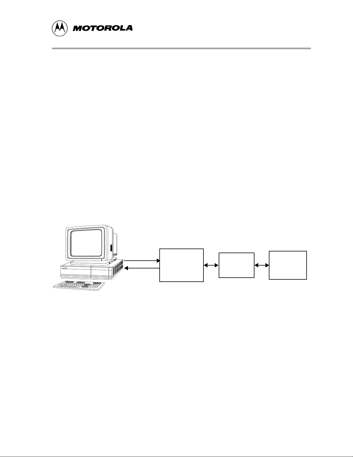
Figure 1-2 shows a functional overview of the system.
RS-232
PC Host
ICS Interface MCU
Figure 1-2. ICS Functional Overview
Voltage
Adjustment
M68ICS08ABUM/D 1-5
Page 14

CHAPTER 1 – INTRODUCTION
1.3.2 MCU Subsystem
The MCU subsystem consists of the MC68HC908AB32 microcontroller,clock
generation , monitor mode control logic that places and holds the ABICS in
monitor mode, the bus voltage level translation buffers, and processor
operating voltage variable regulator.
1.3.2.1 Block Diagram of Simulator Board
Figure 1-3 shows a block diagram of the ABICS simulator board. The
individual blocks are described in the subsections following the diagram.
Figure 1-3. MC68HC908AB32 In-Circuit Simulator Block Diagram
1-6 M68ICS08ABUM/D
Page 15

1.3.2.2 M68HC908AB32 MCU
The MCU is an MC68HC908AB32 and is available in one package only:
• 64-pin QFP
The QFP package mounts in a clam-shell socket.
The on-board MCU (the test MCU) simulates and debugs the MCU’s interface
to its peripherals and to other devices on the target board through a variety of
connections. Depending on the connection, the MCU is used in one of three
operating modes:
• In the ICS socket for programming and simple simulation
• In the socket and connected to the target for emulation
• On the target for MON08 debug operation
1.3.2.3 Clocks
CHAPTER 1 – INTRODUCTION
The ABICS contains a 4.1952-MHz crystal oscillator. When the remote target
connection is made, the user may opt to feed the output from the ABICS
crystal (SP-OSC) to the external clock input (OSC1) of the ABICS via W5, a
2-pin shunt.
1.3.2.4 Board Reset
The ABICS includes two reset sources:
• An output from the POR (Power-On Reset) circuit via the host system
software
• An internal reset exception operation of the processor
The host system resets the ICS by cycling power to most of the ICS circuitry,
including the POR circuit. RS-232 handshake line DTR is used for this
purpose.
The RESET function of the ABICS is both an input and an output. The ABICS
drives its RESET pin low after encountering several different exception
conditions. W3 is providedto allowyou to select whether the target system can
reset the MCU on the ABICS (jumper between pins 1 and 2) or whether the
target system receives a reset signal from the ABICS (jumper between pins 2
and 3).
M68ICS08ABUM/D 1-7
Page 16

CHAPTER 1 – INTRODUCTION
RST* is not a bidirectional, open-drain signal at the target connectors.
Removing the jumper leaves the RST-IN* signal pulled up to MCU operating
voltage.
1.3.2.5 Device Configuration Selection
The operation mode of the ABICS processor is selected at the rising edge of
the RESET signal. The ABICS requires that the processor operate in monitor
mode. To set monitor mode operation, the IRQ* line to the ABICS is level
shiftedtoapplyVHIto the processor on the rising edge of reset. The VHIis a
signal name that is specified as minimum VDD+ 2.5 V and maximum 9 V, with
the highest VDDof 3.3 V, which gives a range of minimum 5.8 V and
maximum 9 V.
The ABICS RST* pin is the main mode select input and is pulled to logic 0,
then logic 1 (processor VDD), to select MCU monitor mode. The host software
must communicate security bytes to the MCU to resume execution out of reset.
Communication to the monitor ROM is via standard, non-return-to-zero (NRZ)
mark/space data format on PTA0. The MCU maintains monitor mode and
disables the COP module through continued application of VHIon either IRQ*
or RST*.
Six commands may be issued by the host software in control of the MCU in
monitor mode: read, write, iread, iwrite, readsp,andrun. Each
command is echoed back through PTA0 for error checking. These commands
are described in the M68ICS08AB IN-CIRCUIT SIMULATOR SOFTWARE
OPERATOR’S MANUAL.
The MCU bus clock is CGMXCLK/2.
1.3.2.6 Level Translation
The ABICS has an operation voltage range of +3.0 to +5.0 volts while the host
developmentsystem interface is an RS-232 (com) port. U2 on the ICS converts
5 V logic signals to RS-232 levels. Transistors Q9-Q10 translate 5 V logic
levels to the MCU operating voltage (3.0-5.0 V).
1-8 M68ICS08ABUM/D
Page 17

1.3.2.7 ABICS Operating Voltage, Variable Selector
To provide the ABICS with power input that matches your target environment,
the ABICS includes a on-board regulator. The ABICS monitors the user’s
target system power via the EVDD pin of FLEX cable. EVDD pin is connected
to power supply of user’s target system via target adapter. If the EVDD pin is
floated, the regulator output 5.0Vdc. The ABICS doesn’t power the target
system.
The on-board regulator is activated by the RS-232 handshake line DTR. To
activate the regulator mannually, set jumper W9.
1.3.2.8 Host System Connector
The host system interface is via a 9-pin DB-9 serial connection plug DEKL9SAT-F.
CHAPTER 1 – INTRODUCTION
M68ICS08ABUM/D 1-9
Page 18

CHAPTER 1 – INTRODUCTION
1.3.2.9 Target Interface Connector
The user target interface connector is two 40-pin shrouded headers (J1, J2).
Table 1-3 shows the target interface pins.
Table 1-3. Target Interface J1
Pin Description Pin Description
1 GND 2 TGT_IRQ*
3PTC24GND
5TGT_PTC06 PTF1
7 NC 8 PTF3
9 VDD 10 NC
11 LVDD 12 PTF5
13 PTD7 14 PTB7
15 PTD5 16 PTD1
17 PTH1 18 AVSS/VREFL
19 GND 20 PTD3
21 PTB2 22 PTA7
23 PTB4 24 GND
25 PTB6 26 PTA4
27 NC 28 PTA2
29 NC 30 TGT_PTA0
31 PTF6 32 PTG2
33 PTE1 34 PTG0
35 PTE3 36 GND
37 PTE5 38 GND
39 PTE7 40 GND
1-10 M68ICS08ABUM/D
Page 19

CHAPTER 1 – INTRODUCTION
Table 1-4. Target interface J2
Pin Description Pin Description
1PTC52PTC4
3TGT_PTC34 RST*
5TGT_PTC16 PTF0
7OSC18PTF2
9 GND 10 PTF4
11 GND 12 PTF7
13 VREFH 14 GND
15 PTD6 16 PTD0
17 PTD4 18 VDDAREF
19 PTH0 20 PTD2
21 PTB1 22 PTB0
23 PTB3 24 PTA6
25 PTB5 26 PTA5
27 GND 28 PTA3
29 NC 30 PTA1
31 NC 32 GND
33 PTE0 34 PTG1
35 PTE2 36 EVDD
37 PTE4 38 GND
39 PTE6 40 GND
M68ICS08ABUM/D 1-11
Page 20

CHAPTER 1 – INTRODUCTION
1.4 TARGET CABLES
A generic cable (Motorola part number M68CLB05C) connects between the
ICS module and target adapter(s) for the different user package targets.
1.4.1 FLEX Cable
The FLEX cable connects to the host system through the appropriate target
head adapter.
1.4.1.1 Cable Connections
Table 1-5 shows the connectivity between the two ends of the FLEX cable and
the usage of the lines in this application.
Table 1-5. FLEX Cable Connectors
M68ICS08AB
Single
PTC4 NA 2 1
PTC5 NA 1 2
TGT_IRQ* 2NA3
GND 1NA4
TGT_RST* NA 4 5
TGT_PTC3 NA 3 6
GND 4NA7
PTC2 3NA8
PTF0 NA 6 9
TGT_PTC1 NA 5 10
PTF1 6NA11
TGT_PTC0 5NA12
PTF2 NA 8 13
Connector P1 Pin
Number
M68ICS08AB
Connector P2 Pin
Number
Target Head
Adapter Pin
Number
OSC1 NA 7 14
PTF3 8NA15
NC 7NA16
1-12 M68ICS08ABUM/D
Page 21

CHAPTER 1 – INTRODUCTION
Table 1-5. FLEX Cable Connectors
M68ICS08AB
Single
PTF4 NA 10 17
GND 19 NA 18
NC 10 NA 19
VDD 9NA20
PTF7 NA 12 21
GND NA 11 22
PTF5 12 NA 23
LVDD 11 NA 24
GND 24 NA 25
VERFH NA 13 26
PTB7 14 NA 27
PTD7 13 NA 28
PTD0 NA 16 29
Connector P1 Pin
Number
M68ICS08AB
Connector P2 Pin
Number
Target Head
Adapter Pin
Number
PTD6 NA 15 30
PTD1 16 NA 31
PTD5 15 NA 32
VDDAREF NA 18 33
PTD4 NA 17 34
VERFL 18 NA 35
PTH1 17 NA 36
PTD2 NA 20 37
PTH0 NA 19 38
PTD3 20 NA 39
GND 38 NA 40
PTB1 NA 21 41
PTB0 NA 22 42
PTB2 21 NA 43
M68ICS08ABUM/D 1-13
Page 22

CHAPTER 1 – INTRODUCTION
Table 1-5. FLEX Cable Connectors
M68ICS08AB
Single
PTA7 22 NA 44
PTB3 NA 23 45
PTA6 NA 24 46
PTB4 23 NA 47
GND 40 NA 48
PTB5 NA 25 49
PTA5 NA 26 50
PTB6 25 NA 51
PTA4 26 NA 52
GND NA 9 53
PTA3 NA 28 54
NC 27 NA 55
PTA2 28 NA 56
Connector P1 Pin
Number
M68ICS08AB
Connector P2 Pin
Number
Target Head
Adapter Pin
Number
NC NA 29 57
PTA1 NA 30 58
NC 29 NA 59
TGT_PTA0 30 NA 60
NC NA 31 61
GND NA 14 62
PTF6 31 NA 63
PTG2 32 NA 64
PTE0 NA 33 65
PTG1 NA 34 66
PTE1 33 NA 67
PTG0 34 NA 68
PTE2 NA 35 69
EVDD NA 36 70
1-14 M68ICS08ABUM/D
Page 23

CHAPTER 1 – INTRODUCTION
Table 1-5. FLEX Cable Connectors
M68ICS08AB
Single
PTE3 35 NA 71
GND 36 NA 72
PTE4 NA 37 73
GND NA 27 74
PTE5 37 NA 75
GND NA 32 76
PTE6 NA 39 77
GND NA 38 78
PTE7 39 NA 79
GND NA 40 80
Connector P1 Pin
Number
M68ICS08AB
Connector P2 Pin
Number
Target Head
Adapter Pin
Number
M68ICS08ABUM/D 1-15
Page 24

CHAPTER 1 – INTRODUCTION
1.4.1.2 Mechanical
The FLEX cable has two 2 ´ 40, 100mil connectors (P1, P2) at the end, which
connects to the ICS module. At the opposite end, it has two 2 ´ 20, 50mil
connector (P3), which connects to the target adapter.
1.4.2 MON08 Cable
The 16-pin MON08 cable connects to header J3 on the M68ICS08AB board
and to pin P1 on the target-system board. Refer to CHAPTER 3 – USING
THE MON08 INTERFACE Cable Connections
Table 1-6 shows the connectivity between the two ends of the MON08 cable
and the usage of the lines in this application.
Figure 1-4. FLEX Cable
T able 1-6. MON08 Cable Connectors
Pin J3 Pin J3
1 RST-OUT* 2 Ground
3 RST-IN* 4 RST*
5 TGT-IRQ* 6 IRQ*
7NC8NC
9TGT-PTA010 PTA0
11 TGT-PTC0 12 PTC0
13 TGT-PTC1 14 PTC1
15 TGT-PTC3 16 PTC3
1.5 ABOUT THIS OPERATOR’S MANUAL
1.5.1 Chapter Organization
This manual covers the M68ICS08AB hardware:
Chapter 2 — Hardware Installation
Chapter 3 —UsingtheMON08Interface
Appendix A— Technical Reference & Troubleshooting
Appendix B— Glossary
1.5.2 Document Conventions
1-16 M68ICS08ABUM/D
Page 25

CHAPTER 1 – INTRODUCTION
This manual uses the following conventions to enhance readability:
• Filenames, program names, code, and commands are indicated in
regular Courier:
SETUP.EXE
MYPDA.ASM
The read and write commands may be issued...
• Functions are indicated in small caps:
The RESET function of the ABICS is both an input and an output.
• Output signals are indicated in Courier:
RST* is not a bidirectional, open-drain signal at the target connectors.
M68ICS08ABUM/D 1-17
Page 26

CHAPTER 1 – INTRODUCTION
1.6 HARDWARE QUICK START INSTRUCTIONS
For users experienced in installing Motorola or other development tools, the
following steps provide a quick start installation procedure for the ABICS
hardware and software.
For more complete hardware instructions, refer to CHAPTER 2 –
HARDWARE INSTALLATION.
1. Install the ICS08AB software package by following the instructions
described in Section 1.5 SOFTWARE QUICK START INSTRUC-
TIONS of the M68ICS08AB IN-CIRCUIT SIMULATOR SOFT-
WARE OPERATOR’S MANUAL.
2. Connect the board.
a. Install the MCU into the M68ICS08AB board.
Locate socket XU1 on the board. Install the MCU (provided with
the M68ICS08AB package) into this socket, observing the pin 1
orientation with the socket’s notch. The top (label side) of the MCU
package must be visible when looking at the component side of the
ABICS board.
b. Connect the ABICS to the host PC.
Locate the 9-pin connector labeled P2 on the ABICS. Using the
cable provided, connect it to a serial COM port on the host PC.
c. Apply power to the ABICS.
Connect the 5-V power supply to the round connector on the
ABICS. Plug the power supply into an AC power outlet, using one
of the country-specific adapters provided. The SYSTEM POWER
LED on the ABICS should light.
1. Complete the installation by following the steps described in Section
1.5 SOFTWARE QUICK START INSTRUCTIONS of the
M68ICS08AB IN-CIRCUIT SIMULATOR SOFTWARE OPERATOR’S MANUAL.
If you experience problems with the quick start procedures, refer to
APPENDIX A TECHNICAL REFERENCE & TROUBLESHOOTING
for troubleshooting instructions.
1.7 CUSTOMER SUPPORT
To obtain information about technical support or ordering parts, call the
Motorola help desk at 800-521-6274.
1-18 M68ICS08ABUM/D
Page 27

2.1 OVERVIEW
This chapter explains how to:
• Configure the M68ICS08AB in-circuit simulator board
• Connect the board to a target system
In interactive mode, the ABICS is connected to the serial port of a host PC.
The actual inputs and outputs of a target system can be used during simulation
of source code.
In stand-alone mode, the ABICS is not connected to the PC. The ICS08ABW
software can be used as a stand-alone simulator. Refer to the M68ICS08AB
IN-CIRCUIT SIMULATOR SOFTWARE OPERATOR’S MANUAL for
detailed information.
Warning: ELECTROSTATIC DISCHARGE PRECAUTION
CHAPTER 2
HARDWARE INSTALLATION
Ordinary amounts of static electricity from your clothing or work
environment can damage or degrade electronic devices and
equipment. For example, the electronic components installed on the
printed circuit board is extremely sensitive to electrostatic
discharge (ESD). Wear a grounding wrist strap whenever handling
any printed circuit board. This strap provides a conductive path for
safely discharging static electricity to ground.
M68ICS08ABUM/D 2-1
Page 28

CHAPTER 2 – HARDWARE INSTALLATION
2.2 CONFIGURING THE IN-CIRCUIT SIMULATOR BOARD
Three configuration headers provide for jumper-selectable hardware options.
Table 2-1, Table 2-2,andTable 2-3 describe these settings.
Note: Factory default settings should be used when following the quick start
procedure described in Section 1.6 HARDWARE QUICK START
INSTRUCTIONS.
Table 2-1. W9 Configuration Header – DTR switch on-board regulator
Pin Signal Name Description
1 PGMRL RS-232 handshaking DTR signal
2 GND To target V
DD
pin
• Jumper on pins 1 and 2
On-board regulator always turn on.
• Jumper off
Default. On-board regulator can be activated by DTR.
Table 2-2. W3 Configuration Header – Target Cable Reset Pin Function
Pin Direction
1inRST_IN* Reset signal from target system: 0 to +5.0
2inorout RST* To/from target RST* pins
3 out RST_OUT* Reset signal to target system: 0 to +5.0 Vdc
Signal
Name
Description
Vdc input to control state of MCU RST* signal
output reflecting state of MCU RST* signal
• Jumper on pins 2 and 3
Default. The target-system’s RESET* is not allowedtoresetthe
MC68ICS08AB MCU.
2-2 M68ICS08ABUM/D
Page 29

Table 2-3. W5 Configuration Header – Oscillator Source
Pin Direction Signal Name Description
1out SP_OSC 4.9152-MHz M68ICS08AB oscillator output
2 in or out OSC1 OSC1 on sockets and target connectors
• Jumper on pins 1 and 2
Default. The M68ICS08AB oscillator is selected.
• Jumper off
Allows using an oscillator on the target system or injecting a different
clock rate at P6 pin 2.
2.3 INSTALLING THE HARDWARE
CHAPTER 2 – HARDWARE INSTALLATION
Before beginning, locate these items:
• 9-pin RS-232 serial connector on the board, labeled P2
• 5-volt circular power-input connector on the ABICS
To prepare the ABICS for use with a host PC:
1. Install the MCU into the M68ICS08AB board.
Locate the socket XU1 on the board.
Install the MCU (provided with the ABICS package) into this socket,
observing the pin 1 orientation with the socket’s notch. The top (label
side) of the MCU package must be visible when looking at the
component side of the board.
2. Connect the board to the host PC.
Locate the 9-pin connector labeled P2 on the board. Using the cable
provided, connect it to a serial COM port on the host PC.
3. Apply power to the board.
Connect the 5-volt power supply to the round connector on the board.
Plug the power supply into an AC power outlet, using one of the
country-specific adapters provided. The ICS PWR LED (Yellow) on
the board should light.
2.4 CONNECTING TO A TARGET SYSTEM
The two ways to connect the M68ICS08AB simulator board to a target system
are:
M68ICS08ABUM/D 2-3
Page 30

CHAPTER 2 – HARDWARE INSTALLATION
1. Using the MCU on the board, break its processor signals out to the target system.
This method allows the board’s MCU (MC68HC908AB32) to control
the target system’s hardware. An MCU must be installed on the
M68ICS08AB board. The target system’s MCU must be removed.
Connector J1, J2 on the board may be used with a flex emulation cable
and target head adapter, which are available separately. Target head
adapters are available for the QFP footprints on the target board.
2. Use the MON08 debug interface for communication with the target
system’s MCU.
This method allows in-circuit FLASH/EEPROM programming and
debugging of the target system’s MCU (MC68HC908AB32). An MCU
must be installed in the target system. The board’s MCU must be
removed.
Connect the board’s MON08 connector with a compatible MON08
connector on the target system. Complete instructions for constructing
this interface on the target board are found in CHAPTER 3 – USING
THE MON08 INTERFACE.
Note: MON08 debug interface is designed for 5-volt operation. To
operate MON08 debug interface at low-voltage, connect power from
target system to EVDD input (Pin 1 of W10). The on-board regulator
will match the power of M68ICS08AB to the target system.
2-4 M68ICS08ABUM/D
Page 31

CHAPTER 3
USING THE MON08 INTERFACE
3.1 OVERVIEW
The MON08 debugging interface may be used to debug and program a target
system’s MCU directly. The target system must be connected to the
M68ICS08AB In-circuit simulator board’s MON08 interface connector. This
chapter explains how to connect to the MON08 interface on the target board.
3.2 HEADER PLACEMENT AND LAYOUT
Two headers must be placed on the target board:
P1 — 16-pin header such as Berg Electronics part number 67997-616
P2 — 1-pin header such as Berg Electronics part number 68001-601
Table 3-2 and Table 3-1 show the target-system interconnections for P1 and
P2. Figure 3-1 shows the pin layouts for P1 and P2. Additional information
about the connections on the ABICS board can be found in APPENDIX A
TECHNICAL REFERENCE & TROUBLESHOOTING.
M68ICS08ABUM/D 3-1
Page 32

CHAPTER 3 – USING THE MON08 INTERFACE
Table 3-1. MON08 Target System Connector P1
Pin #
M68ICS08AB
Label
Direction Target System Connection
1 RST_OUT* out to target Connect to logic that is to receive the RST* signal.
2 GND ground Connect to ground (V
SS
).
3 RST_IN* in from target Connect to all logic that generates resets.
4 RST* bi-directional Connect to MCU RST* pin and P1 pin 1. No other target-
system logic should be tied to this signal. It will swing from 0
to +7.5 Vdc.
5 TGT_IRQ* in from target Connect to logic that generates interrupts.
6 IRQ* out to target Connect to MCU IRQ pin. No other target-system logic
should be tied to this signal. It will swing from 0 to Vdd.
7 NC NC Not Connected
8 NC NC Not Connected
9 TGT_PTA0 bi-directional Connect to user circuit that would normally be connected to
PTA0 on the MCU. This circuit will not be connected to the
MCU when the in-circuit simulator is being used.
10 PTA0 bi-directional Connect to MCU PTA0 pin. No other target-system logic
should be tied to this signal. Host I/O present on this pin.
11 TGT_PTC0 bi-directional Connect to user circuit that would normally be connected to
PTC0 on the MCU.
12 PTC0 bi-directional Connect to MCU PTC0 pin. No other target-system logic
should be tied to this signal. Grounded during reset and for
256 cycles after reset.
13 TGT_PTC1 bi-directional Connect to user circuit that would normally be connected to
PTC1 on the MCU.
14 PTC1 bi-directional Connect to MCU PTC1 pin. No other target-system logic
should be tied to this signal. Grounded during reset.
15 TGT_PTC3 bi-directional Connect to user circuit that would normally be connected to
PTC3 on the MCU.
16 PTC3 bi-directional Connect to MCU PTC3 pin. No other target-system logic
should be tied to this signal. Grounded during reset.
3-2 M68ICS08ABUM/D
Page 33

CHAPTER 3 – USING THE MON08 INTERFACE
Table 3-2. MON08 Target System Connector P2
Pin #
M68ICS08AB
Label
1 RST* bi-directional Connectto MCU RST* pin and P2 pin 4. No other target
Direction Target System Connection
system logic should be tied to this signal. It will swing
from0to+7.5Vdc.
P2
12
15 16
P1
Figure 3-1. MON08 Target System Connector Layout
3.3 CONNECTING TO THE IN-CIRCUIT SIMULATOR
Using the 16-pin cable provided with the ABICS kit, connect one end of the
cable to the ABICS board at P5. Connect the other end to connector P1 on the
target system board. The pin-1 indicators on each cable end must correspond to
the pin-1 indicators on the headers. P2 is not used when connecting to the
ABICS board.
M68ICS08ABUM/D 3-3
Page 34

CHAPTER 3 – USING THE MON08 INTERFACE
3.4 DISABLING THE TARGET-SYSTEM INTERFACE
To use the target system in a stand-alone fashion (without the ABICS board
connected), jumper the pins on the target board’s connectors, as shown in
Figure 3-2. This reconnects the target MCU to the appropriate circuits on the
target system.
P2
12
15 16
P1
Figure 3-2. Target System Stand-Alone Connection
For production boards, a further enhancement of this scheme would be to
include cutable traces between the pins of P1 and P2,asshowninFigure 3-2.
The traces may be cut when debugging is necessary. To return the board to
stand-alone use, jumpers may be installed as shown.
3-4 M68ICS08ABUM/D
Page 35

TECHNICAL REFERENCE & TROUBLESHOOTING
A.1 OVERVIEW
This appendix provides technical support information for the M68ICS08AB
in-circuit simulator kit, including:
• Functional description of the kit
• Troubleshooting the quick-start procedure
• Troubleshooting MON08 mode
• Connector and cable pin assignments
• Schematic diagrams
• Parts list
• Board layout diagram
Caution: ELECTROSTATIC DISCHARGE PRECAUTION
APPENDIX A
Ordinary amounts of static electricity from clothing or the work
environment can damage or degrade electronic devices and
equipment. For example, the electronic components installed on
printed circuit boards are extremely sensitive to electrostatic
discharge (ESD). Wear a grounding wrist strap whenever you
handle any printed circuit board. This strap provides a conductive
path for safely discharging static electricity to ground.
M68ICS08ABUM/D A-1
Page 36

APPENDIX A – TECHNICAL REFERENCE & TROUBLESHOOTING
A.2 FUNCTIONAL DESCRIPTION
The M68ICS08AB hardware consists of one component:
• ICS08AB board
A.2.1 ICS08AB Board
The core component of the board is the MC68HC908AB32 MCU. This MCU
resides either on the ICS08AB board or on a target system.
When the MCU resides on the board, the board may be used as an in-circuit
emulator or simulator for the MC68HC908AB32. For this configuration, a
target cable is run from the board to the target system. A flexible target head
adapter cable (Motorola part number M68CBL05C), terminating in connectors
for target head adapter . For a 64-pin QFP-package MCU on the target system,
use Motorola THA model number M68TC08ABFU64.
When the MCU resides on a target system, the ICS08AB board can
communicate with the MCU over a 16-pin MON08 cable (Motorola part
number 01-RE91008W01). Either version of the MCU is supported when
using the MON08 cable.
When using the ICS08ABZ simulation software, the MCU provides the
required input/output information that lets the host computer simulate code,
performing all functions except for maintaining port values. The internal
FLASH/EEPROM memory on the device is downloaded with a program that
generates the appropriate port values. The ICS08ABZ software on the host
computer lets the host computer become a simulator. When the ICS requires
port data, the computer requests the data through the host's serial connection to
the core MCU. The core MCU responds by sending the data to the host via the
serial connection. It is the arrangement that allows a real-world interface for
the in-circuit simulator. The clock runs the MCU at a 4.9512-MHz external
clock r ate. Note that the simulation speed will be slower than this rate, because
the host computer is the simulator.
When using the ICS08SZ debugging software, your code can be run directly
out of the MCU’s internal FLASH at real-time speeds.
Note: The ICS08AB’s emulation of the MC68HC908AB32 is limited. Port A bit 0
(PTA0) is used for host-to-MCU communication. The port bit is not available
for connection to a target system. Setting DDRA bit 0 to 1 will stop
communications with the simulation or debugger software and will require a
systemresettoregaincommunicationwiththeMCU.PortbitsPTC0, PTC1,
and PTC3 are temporarily disconnected from the target system during reset.
Emulation of the MC68HC908AB32’s RST* signal is also limited in that the
signal is not a bidirectional, open-drain signal. It is emulated as either an input
or an output (determined by jumper header W3) when using the target
A-2 M68ICS08ABUM/D
Page 37

APPENDIX A – TECHNICAL REFERENCE & TROUBLESHOOTING
connectors or as two pins (one input and one output) when using the MON08
cable.
When using the PROG08SZ programming software, the MCU’s FLASH/
EEPROM memory can be programmed. Socket XU1 supports the 64-pin QFP
version of the part. The ICS08AB also supports in-circuit programming of
either version of the part through the MON08 cable.
The ICS08AB board also provides +5 Vdc power, +8.0 Vdc power for the
V
voltage required to enter monitor mode, a 4.9152-MHz clock signal, and
TST
host PC RS-232 level translation.
M68ICS08ABUM/D A-3
Page 38

APPENDIX A – TECHNICAL REFERENCE & TROUBLESHOOTING
A.3 TROUBLESHOOTING THE QUICK START
The quick-start installation procedure in section Section 1.6 HARDWARE
QUICK START INSTRUCTIONS describes how to prepare the ICS08AB
for use in the instances where the MCU is installed on the ICS08AB board.
These instances include:
• Using the ICS08AB as an in-circuit simulator/emulator with a target
cable
• Using the ICS08AB as a programmer
• Using the ICS08AB as a stand-alone system without a target board
If you experience difficulties quick starting the kit using the procedure outlined
in Section 1.6 HARDWARE QUICK START INSTRUCTIONS, follow
these steps:
1. Do not use the MON08 cable to a target system in these modes. The
MON08 cable connection is to be used only when the MCU is on the
target system. Troubleshooting information for the MON08 modes may
be found in Section A.4 TROUBLESHOOTING MON08 MODE.
2. Disconnect any target cables from the board. These troubleshooting
steps assume that no target system connections are present.
3. Make sure that the MCU is installed correctly. Insert the MCU with the
orientation notch and pin 1 to the upper left in the respective socket.
4. Make sure the board is getting power:
a. Check the power at the output of the adapter. First disconnect the
ICS08AB from the power supply, then measure the power at the
wall adapter’s output connector to confirm that it produces 5 Vdc.
The outer barrel of the connector is ground, and the inner sleeve is
+5 Vdc. If there is no power at the connector,verify that the adapter
is getting power from the AC power outlet.
b. Check the power at the ICS08AB board. Plug the adapter’s output
connector into the ICS08AB. The MCU PWR LED (Yellow) should
light. Check for 5 Vdc at the ICS08AB’s fuse F1. If the LED does
not light or if 5 Vdc is not present on fuse F1, check the fuse in the
ICS08AB. If more than 6.2 Vdc or reverse voltage is applied to the
ICS08AB, the fuse will blow.
c. Check the ICS08AB MCU PWR. Disconnect the ICS08AB from
the power supply and from the host PC. Configure the ICS08AB
board to the factory defaults. Reconnect the power supply to the
ICS08AB. The MCU PWR LED should light. If the LED does not
light, there may be a problem with the ICS08AB causing too much
of a drain on the 5 Vdc supply.
A-4 M68ICS08ABUM/D
Page 39

APPENDIX A – TECHNICAL REFERENCE & TROUBLESHOOTING
d. Check the MCU PWR at test point TP3 (MCU-VDD). Usingthe side
pin on P1 (DC INPUT jack) as the ground reference, check for
5.0Vdc at TP3.
e. Check the ICS08AB board’s V
power with the host discon-
TST
nected. With the ICS08AB board powered, and no host connection
to the ICS08AB, install jumper on W9 to activate on-board regulator, check for the following voltages on the ICS08AB board, using
the side pin on P1 (DC INPUT jack) as the ground reference:
Approximately 8.0 Vdc at TP1 (VTST_IRQ)
Approximately 8.0 Vdc at TP2 (VTST_RST)
If this voltage is not present when the MCU PWR LED is lit, there
may be a problem with the ICS08AB’s internal step-up power supply. Remove jumper on W9 to activate on-board regulator by DTR.
f. Check the ICS08AB board’s V
power with the host connected.
TST
First, exit any ICS08ABZ software that may be running on the host
PC. Then disconnect power from the ICS08AB. Ensure that the
ICS08AB board is configured for the factory default settings.
Ensure that there is an MCU in XU1 and that it is inserted correctly.
Connect the serial cable between the host PC and the ICS08AB.
Apply power to the ICS08AB. At this point, the ICS PWR LED
(Green) should be lit, and the MCU PWR LED (Yellow) should be
off. If the MCU PWR LED is on, there may be a problem with the
host PC’s serial port or the serial cable. See step 5 for communications problems. If the MCU PWR LED is off, start the ICS08ABZ
simulator software as described in Section 1.6 HARDWARE
QUICK START INSTRUCTIONS while watching the MCU PWR
LED.
If the MCU PWR LED does not light at all, there may be a problem
with the host PC communicating with the board. Refer to step 5.
If the MCU PWR LED flickers a few times and then goes out, the
host PC is able to control the power to the ICS08AB board but
communications may still not be established with the MCU. As the
flickering of the MCU PWR LED indicates, the host PC is applying
and removing power to the ICS08AB board during this period. Use
an oscilloscope to view the voltages on TP1,TP2andTP3 as the
software tries to establish communication with the MCU. Restart or
retry the ICS08ABZ software while looking at the signals. Using
the side pin on P1 (DC INPUT jack) as the ground reference, check
for a signal that varies between 0 and +5 Vdc at TP3 (MCU-VDD)
and between 0 and +8.0 Vdc at TP1 (VTST_IRQ) and TP2
M68ICS08ABUM/D A-5
Page 40

APPENDIX A – TECHNICAL REFERENCE & TROUBLESHOOTING
(VTST_RST). If these voltages are present, the power is good, but
communication problems should be investigated as described in
step 5.
If the MCU PWR LED comes on and stays on, communication was
probably established with the MCU. Check for the following voltages, using the side pin on P1 (DC INPUT jack) as the ground reference:
Approximately 9.0 Vdc at TP1 and TP2
Approximately 5.0 Vdc at TP3
If these voltages are present, the power is good, and the problem
lies elsewhere.
5. Make sure that the host PC can communicate with the MCU:
a. The MCU’s PTA0 pin is used for host communications. DDRA bit 0
should never be set to 1 as this interrupts monitor-mode communications. The target connector PTA0 pin (J1 pin 30) is never connected to the MCU’s PTA0 pin. They are wired only for probing
purposes.
b. Make sure that the serial cable is correctly attached to the ICS08AB
and to the correct serial port on the host computer.
c. Make sure that the cable is a straight-through cable supporting all
nine pins of the serial port connection.
d. Make sure that no hardware security key or other devices are
attached to the serial port or cable.
e. Make sure that the host PC supports the minimum speed require-
ments of the ICS08ABZ software.
f. Make sure to use the correct security code to access the MCU. If
you have previously programmed the security bytes, the part will
not unlock and enter monitor mode unless the correct security code
is sent to the MCU.
g. Check for data at the ICS08AB end of the serial cable. Pin 3 of this
connector carries RS-232 data into the ICS08AB; pin 2 carries RS232 data out of the ICS08AB. Pin 4 controls the MCU PWR. Pin 5
is ground. While the ICS08ABZ software is trying to establish
communications, pins 3 and 4 should both toggle between +10 Vdc
and –10 Vdc (or +12 Vdc and –12 Vdc). If you do not see these signals at the cable end, the problem is on the PC and cable side of the
system. When connected to the ICS08AB, a +10 Vdc signal on pin
4 should activate the ICS08AB and the MCU PWR LED.
A-6 M68ICS08ABUM/D
Page 41

APPENDIX A – TECHNICAL REFERENCE & TROUBLESHOOTING
h. Make sure the serial data is getting to the MCU’s PTA0 pin. First,
exit any ICS08ABZ software that may be running on the host PC.
Then disconnect power from the ICS08AB. Ensure that the
ICS08AB board is configured for the factory default settings.
Ensure that there is an MCU in XU1 and that it is inserted correctly.
Connect the serial cable between the host PC and the ICS08AB.
Apply power to the ICS08AB. Start the ICS08ABZ simulator software as described in Section 1.6 HARDWARE QUICK START
INSTRUCTIONS. Probe the PTA0 pin (XU1 pin26orJ3pin10)
for the serial data. Since the board power is turned off and on several times during the connecting phase, the data observed at the
MCU’s PTA0 pinisalsoaffected.
6. Make sure that the MCU has a good clock source. Use an oscilloscope
to check the OSC1 input at the MCU (XU1 pin 59). Set the oscilloscope
to 0.1 ms per division. The oscillator should run when the MCU PWR
LED is on. You should observe approximately 2 divisions per cycle.
This corresponds to a 4.9152-MHz signal; the frequency required for a
9600-baud communications rate. If the clock signal is not present,
check to see that a jumper is installed on W5. This selects the ICS08AB
as the source of the OSC1 signal.
7. Make sure that the MCU can enter and remain in monitor mode. For
this to happen, the following conditions must occur:
a. At the rising edge of RST*, IRQ* must be at V
(8.0 Vdc).
TST
Using a dual-trace oscilloscope, trigger channel 1 on the rising edge
of RST* (XU1 pin 3) and read the IRQ* pin (XU1 pin 2) with channel 2. Start the ICS08ABZ software as described in Section 1.6
HARDWARE QUICK START INSTRUCTIONS and verify
that the IRQ* signal is approximately 8.0 Vdc when RST* rises. If
IRQ* is not at 8.0 Vdc, there may be a problem with the ICS08AB
board’s IRQ circuit. Check D10 and R38 for the proper signals to
keep IRQ* at 8.0 Vdc during the period where RST* is low.
b. At the rising edge of RST*, PTA0, PTC0, PTC1,andPTC3 must
be held at logic values 1, 1, 0, and 0, respectively. The logic levels
are 5.0 V CMOS logic levels (with the factory default setting and
don’t connect ICS08AB to target system). Using a dual-trace oscil-
loscope, trigger channel 1 on the rising edge of RST* (XU1 pin 3),
and read the corresponding MCU pin with channel 2. PTA0 (XU1
pin 26) is the serial data pin to and from the host PC and should be
around 5.0 Vdc at the rising edge of RST*. PTC0 (XU1 pin 60),
PTC1 (XU1 pin 61), and PTC3 (XU1 pin 63) are controlled by analog switch U5 and should be approximately 5.0 V, 0 V and 0 V,
respectively, at the rising edge of RST*. Port pins PTC0, PTC1,
M68ICS08ABUM/D A-7
Page 42

APPENDIX A – TECHNICAL REFERENCE & TROUBLESHOOTING
and PTC3 are connected to the target connector pins after the rising
edge of RST* and are then available for target system connections.
The MCU’s PTA0 pin is never connected to the target pins, as it is
used for host communication.
c. IRQ* must remain at 8.0 Vdc to hold the MCU in monitor mode.
The ICS08AB board has an interrupt lockout feature to keep IRQ*
at 8.0 Vdc when the RST* or RST_IN* signal is asserted (low)
and keep it at 8.0 Vdc until after RST* goes high. The TGT_IRQ*
signal is allowed to control the IRQ* signal when RST* is not
asserted.
8. Make sure that external circuitry does not interfere with the monitor
mode communications. When connecting external circuitry to the
ICS08AB board, use only the target system connectors J1 and J2.
This ensures that the target system will not interfere with the communications and setup of the MCU’s monitor mode by allowing the
ICS08AB to disconnect some target system components during monitor mode entry.
9. When connecting to a target system, observe the setting of W3 (target
RST* direction). W3 is provided to allow you to select whether the target system can reset the MCU on the ICS08AB (jumper between pins 1
and 2) or whether the target system receives a reset signal from the
ICS08AB (jumper between pins 2 and 3). RST* is not a bidirectional,
open-drain signal at the target connectors. Removing the jumper leaves
the RST_IN* signal pulled up to 5 Vdc.
A.4 TROUBLESHOOTING MON08 MODE
This section describes the troubleshooting steps for the instances where the
MCU is installed on a target system and the ICS08AB is used to interact with
the target system through the MON08 cable. These instances include in-circuit
simulation/emulation and FLASH memory programming through the MON08
cable.
1. Disconnect the target system and make sure that the ICS08AB operates
correctly when configured as described in the quick start instructions
(Section 1.6 HARDWARE QUICK START INSTRUCTIONS).
Refer to Section A.3 TROUBLESHOOTING THE QUICK START
if you have trouble getting the quick start to work.
2. If the quick start works, the ICS08AB should be functioning well
enough to place the MCU on the target system into monitor mode.
3. Prepare the ICS08AB for use with the MON08 cable. Turn off the
power to the target system. Exit the ICS08AB software. Remove the
A-8 M68ICS08ABUM/D
Page 43

APPENDIX A – TECHNICAL REFERENCE & TROUBLESHOOTING
power plug from the ICS08AB. RemoveanyMCUfromsockets
XU1
.
Jumper selections on W4 have no effect when using the MON08 cable.
4. Connect the 16-pin cable from J3 on the ICS08AB to the target sys-
tem’sMON08 connector. Details on designing a MON08 connector for
the target system are given in CHAPTER 3 – USING THE MON08
INTERFACE. If cutable jumpers were used on the target board, the
jumpers must be cut before using the MON08 cable.
5. The target system (including the MCU) must be externally powered.
The target system’s MCU VDDmust match the MCU-VDD setting on
the ICS08AB to communicate with the ICS08AB. If the target system
is not powered by 5 Vdc, connect target system’s Vdd to EVDD input
(W10 pin 1) on the ICS08AB. The on-board regulator adjust the MCU-
VDD to match the Vdd setting on the target system.
6. Exit any ICS08ABZ software that may be running on the host PC. Con-
nect the serial cable between the host PC and the ICS08AB. Apply
power to the ICS08AB by connecting the wall adapter’s output jack to
the ICS08AB. At this point, the ICS PWR LED (Green) should be lit,
and the MCU PWR LED (Yellow) should be off. If the MCU PWR LED
is on, there may be a problem with the host PC’s serial port or the serial
cable. Refer to step 9 for information on host communications.
7. Apply power to the target system. At this point, the target MCU should
be powered. Check for the appropriate voltage at the MCU’s VDDpin.
The ICS08AB should leave the targetMCU in reset with approximately
0VdcattheMCU’sRST* pin. Verify this at the target MCU’s RST*
pin and at J3 pin 4. If RST* floats too high, the MCU may start up and
begin executing code out of its FLASH memory. The ICS08AB should
reset the MCU again in step 8 when the software is started.
8. Start the ICS08ABZ simulator software as described in Section 1.6
HARDWARE QUICK START INSTRUCTIONS while watching
the MCU PWR LED.
If the MCU PWR LED does not light at all, there may be a problem with
the host PC communicating with the ICS08AB. Continue with step 9.
If the MCU PWR LED flickers a few times and then goes out, the host
PC is able to control the ICS08AB but communications may still not be
established with the MCU on the target system. As the flickering of the
MCU PWR LED indicates, the host PC is applying and removing power
to the ICS08AB board during this period. If the MCU PWR LED stays
on, the power is good, but the MCU is not being placed in monitor
mode. Continue with step 9.
M68ICS08ABUM/D A-9
Page 44

APPENDIX A – TECHNICAL REFERENCE & TROUBLESHOOTING
9. Make sure the host PC can communicate with the MCU:
a. The MCU’s PTA0 pin is used for host communications. DDRA bit 0
should never be set to 1, as this interrupts monitor-mode communications. The MON08 pin TGT_PTA0 (J3 pin 9) is never connected
to the MCU’s PTA0 pin. It is wired to XU1 pin 30 for probing pur-
poses. On the MON08 connector J3, pin 10 is wired to the MCU’s
PTA0 pin. Driving this signal with external logic on the target system will interrupt communications.
b. Make sure that the MON08 cable is properly installed between the
ICS08AB and the target system. Pin 1 of each connector on the
cable must go to pin 1 of the headers on the ICS08AB and target
system.
c. Make sure that the serial cable is correctly attached to the ICS08AB
and to the correct serial port on the host computer.
d. Make sure that the cable is a straight-through cable supporting all
nine pins of the serial-port connection.
e. Make sure that no hardware security key or other device is attached
to the serial port or cable.
f. Make sure that the host PC supports the minimum speed require-
ments of the ICS08ABZ software.
g. Make sure to use the correct security code to access the MCU. If
you have previously programmed the security bytes, the part will
not unlock and enter monitor mode unless the correct security code
is sent to the MCU.
h. Make sure the serial data is getting to the MCU’s PTA0 pin. Re-
start the ICS08ABZ simulator software as described in sections 3
and 4 of the quick-start instructions. Probe the PTA0 pin of the target MCU for the serial data. Since the board power is turned off and
on several times during the connecting phase, the data observed at
the MCU’s PTA0 pinisalsoaffected.
i. Make sure that the target MCU has a good clock source. Use a
clock rate that gives a 9600-baud serial communications rate for
monitor mode on the target system. Use an oscilloscope to check
the OSC2 output at the MCU. Set the oscilloscope to 0.1 ms per
division. The oscillator should run when the MCU PWR LED is on.
There should be approximately two divisions per cycle. This corresponds to a 4.9152-MHz signal, the frequency required for a 9600baud communications rate. If the clock signal is not present, check
to see that a jumper is installed on W5. This selects the ICS08AB as
the source of the OSC1 signal.
A-10 M68ICS08ABUM/D
Page 45

APPENDIX A – TECHNICAL REFERENCE & TROUBLESHOOTING
10. Make sure that the MCU can enter and remain in monitor mode. For
this to happen, the following conditions must occur:
a. At the rising edge of RST*, the target MCU’s IRQ* pin must be at
V
(8.0 Vdc). Using a dual-trace oscilloscope, trigger channel 1
TST
on the rising edge of the MCU’s RST* pin and read the IRQ* pin
with channel 2. Start the ICS08ABZ software as described in Sec-
tion 1.6 HARDWARE QUICK START INSTRUCTIONS and
verify that the IRQ* signal is approximately 8.0 Vdc when RST*
rises.
b. At the rising edge of RST*, PTA0, PTC0, PTC1,andPTC3 must
be held at logic values 1, 1, 0, and 0, respectively. The logic levels
are 5.0 V CMOS logic levels (with the factory default setting, and
5.0 Vdc EVDD input or left EVDD input floating) Using a dualtrace oscilloscope, trigger channel 1 on the rising edge of RST* and
read the corresponding MCU pin with channel 2. PTA0 is the serial
data pin to and from the host PC and should be held at logic value 1
at the rising edge of RST*. PTC0, PTC1,andPTC3 are controlled
by analog switch U5 on the ICS08AB and should be approximately
5.0 V, 0 V, and 0 V respectively, at the rising edge of RST*.After
the rising edge of RST*, the MCU pins PTC0, PTC1,andPTC3
are connected (by the ICS08AB) to the MON08 connector pins
TGT_PTC0, TGT_PTC1,andTGT_PTC3, respectively. The
MCU’s PTA0 pin is never connected to the target pins, as it is used
for host communication.
c. IRQ* must remain at 8.0 Vdc to hold the MCU in monitor mode.
The ICS08AB board has an IRQ* lockout feature to keep IRQ* at
8.0 Vdc when the RST* or RST_IN* signal is asserted (low) and
to keep it at 8.0 Vdc until after RST* goes high. The TGT_IRQ*
signal is allowed to control the IRQ* signal when RST* is not
asserted.
11. Make sure that the target circuitry does not interfere with the monitor
mode communications. When connecting target circuitry to the MCU,
be sure to connect the circuits through the ICS08AB by connecting to
the RST_OUT*, RST_IN*, TGT_IRQ*, TGT_PTA0, TGT_PTC0,
TGT_PTC1,andTGT_PTC3 pins of the MON08 connector. These sig-
nals will be connected by the ICS08AB to the corresponding pins of the
MCU through the corresponding MON08 connector pins—RST*,
IRQ*, PTC0, PTC1,andPTC3—after monitor mode is established.
TGT_PTA0 is never connected to PTA0,asthePTA0 signal is being
used for host communications.
M68ICS08ABUM/D A-11
Page 46

APPENDIX A – TECHNICAL REFERENCE & TROUBLESHOOTING
A.5 CONNECTOR PIN ASSIGNMENTS
The tables in this section describe the pin assignments for the connector on the
ICS08AB board.
Table A-1. Target Connector P7
Pin
No.
Board
Label
MCU
Mnemonic
Schematic
Direct to MCU
Sockets?
Dir Signal Description
1
2
3
4
5
6
7
8
9
10
11
12
13
14
15
GND
T_IRQ
*
PTC2
GND
PTC0
PTF1
NC
PTF3
VDD
NC
LVDD
PTF5
PTD7
PTB7
PTD5
Vss GND Yes Gnd MCU ground
IRQ* TGT-IRQ* No In External interrupt
PTC2 PTC2 Yes Bidir Port C I/O – bit 2
Vss GND Yes Gnd ICS/MCU ground
PTC0 TGT_PTC0 Yes, after reset Bidir Port C I/O – bit 0
PTF1 PTF1 Yes Bidir Port F I/O – bit 1
None None No NC No connection
PTF3 PTF3 Yes Bidir Port F I/O – bit 3
None VDD No Pwr ICS power
None None No NC No connection
V
DD
PTF5 PTF5 Yes Bidir Port F I/O – bit 5
PTD7 PTD7 Yes Bidir Port D I/O – bit 7
PTB7 PTB7 Yes Bidir Port B I/O – bit 7
PTD5 PTD5 Yes Bidir Port D I/O – bit 5
LVDD Yes Pwr MCU power
16
PTD1
17
PTH1
18
VERFL
19
GND
20
PTD3
21
PTB2
22
PTA7
23
PTB4
24
GND
A-12 M68ICS08ABUM/D
PTD1 PTD1 Yes Bidir Port D I/O – bit 1
PTH1 PTH1 Yes Bidir Port H I/O – bit 1
AVSS/
VERFL
Vss GND Yes Gnd ICS/MCU ground
PTD3 PTD3 Yes Bidir Port D I/O – bit 3
PTB2 PTB2 Yes Bidir Port B I/O – bit 2
PTA7 PTA7 Yes Bidir Port A I/O – bit 7
PTB4 PTB4 Yes Bidir Port BI/O – bit 4
Vss GND Yes Gnd ICS/MCU ground
AVSS/
VERFL
Yes Gnd ADC ground
Page 47

APPENDIX A – TECHNICAL REFERENCE & TROUBLESHOOTING
Pin
No.
25
26
27
28
29
30
31
32
33
34
35
Board
Label
PTB6
PTA4
NC
PTA2
NC
PTA0
PTF6
PTG2
PTE1
PTG0
PTE3
Table A-1. Target Connector P7
MCU
Mnemonic
PTB6 PTB6 Yes Bidir Port BI/O – bit 6
PTA4 PTA4 Yes Bidir Port A I/O – bit 4
None None No NC No connection
PTA2 PTA2 Yes Bidir Port A I/O – bit 2
None None No NC No connection
PTA0 TGT_PTA0 No, only to P5 Bidir Port A I/O – bit 0,
PTF6 PTF6 Yes Bidir Port F I/O – bit 6
PTG2 PTG2 Yes Bidir Port G I/O – bit 2
PTE1 PTE1 Yes Bidir Port E I/O – bit 1
PTG0 PTG0 Yes Bidir Port G I/O – bit 0
PTE3 PTE3 Yes Bidir Port E I/O – bit 3
Schematic
Direct to MCU
Sockets?
(Continued)
Dir Signal Description
Unavailable MCU
connection
36
37
38
39
40
GND
PTE5
GND
PTE7
GND
Vss GND Yes Gnd ICS/MCU ground
PTE5 PTE5 Yes Bidir Port E I/O – bit 5
Vss GND Yes Gnd ICS/MCU ground
PTE7 PTE7 Yes Bidir Port E I/O – bit 7
Vss GND Yes Gnd ICS/MCU ground
M68ICS08ABUM/D A-13
Page 48

APPENDIX A – TECHNICAL REFERENCE & TROUBLESHOOTING
Table A-2. Target Connector P8
Pin
Board
No.
Label
1 PTC5 PTC5 PTC5 Yes Bidir Port C I/O – bit 5
2 PTC4 PTC4 PTC4 Yes Bidir Port C I/O – bit 4
3 PTC3 PTC3 TGT_PTC3 Yes, after reset Bidir Port C I/O – bit 3
MCU
Mnemonic
Schematic
NET
Direct to MCU
Sockets?
Dir Signal Description
4 RST* RST* RST* No, P4 pin 2 In or
out
5 PTC1 PTC1 TGT_PTC1 Yes, after reset Bidir Port C I/O – bit 1
6 PTF0 PTC0 TGT_PTC0 Yes, after reset Bidir Port C I/O – bit 0
7 OSC1 OSC1 OSC1 Yes In Crystal amplifier input
8 PTF2 PTF2 PTF2 Yes Bidir Por t F I/O – bit 2
9 GND Vss GND Yes Gnd ICS/MCU ground
10 PTF4 PTF4 PTF4 Yes Bidir Port F I/O – bit 4
11 GND Vss GND Yes Gnd ICS/MCU ground
12 PTF7 PTF7 PTF7 Yes Bidir Port F I/O – bit 7
13 VERFH VERFH VERFH Yes In ADC reference
14 GND Vss GND Yes Gnd ICS/MCU ground
15 PTD6 PTD6 PTD6 Yes Bidir Port D I/O – bit 6
16 PTD0 PTD0 PTD0 Yes Bidir Port D I/O – bit 0
17 PTD4 PTD4 PTD4 Yes Bidir Port D I/O – bit 4
External reset
18 VDDAREFVDDADRF VDDADRF Yes Pwr ADC power
19 PTH0 PTH0 PTH0 Yes Bidir Port H I/O – bit 0
20 PTD2 PTD2 PTD2 Yes Bidir Port D I/O – bit 2
21 PTB1 PTB1 PTB1 Yes Bidir Port B I/O – bit 1
22 PTB0 PTB0 PTB0 Yes Bidir Port B I/O – bit 0
23 PTB3 PTB3 PTB3 Yes Bidir Port B I/O – bit 3
24 PTA6 PTA6 PTA6 Yes Bidir Port A I/O – bit 6
25 PTB5 PTB5 PTB5 Yes Bidir Port B I/O – bit 5
26 PTA5 PTA5 PTA5 Yes Bidir Port A I/O – bit 5
A-14 M68ICS08ABUM/D
Page 49

APPENDIX A – TECHNICAL REFERENCE & TROUBLESHOOTING
Table A-2. Target Connector P8
Pin
Board
No.
Label
27 GND Vss GND Yes Gnd ICS/MCU ground
28 PTA3 PTA3 PTA3 Yes Bidir Port A I/O – bit 3
29 NC None None No NC No connection
30 PTA1 PTA1 PTA1 Yes Bidir Port A I/O – bit 1
31 NC None None No NC No connection
32 GND Vss GND Yes Gnd ICS/MCU ground
33 PTE0 PTE0 PTE0 Yes Bidir Port E I/O – bit 0
34 PTG1 PTG1 PTG1 Yes Bidir Port G I/O – bit 1
35 PTE2 PTE2 PTE2 Yes Bidir Port E I/O – bit 2
36 EVDD EVDD EVDD No In Target power, reference
37 PTE4 PTE4 PTE4 Yes Bidir Port E I/O – bit 4
MCU
Mnemonic
Schematic
NET
Direct to MCU
Sockets?
(Continued)
Dir Signal Description
of on-board voltage
regulator.
38 GND Vss GND Yes Gnd ICS/MCU ground
39 PTE6 PTE6 PTE6 Yes Bidir Port E I/O – bit 6
40 GND Vss GND Yes Gnd ICS/MCU ground
M68ICS08ABUM/D A-15
Page 50

APPENDIX A – TECHNICAL REFERENCE & TROUBLESHOOTING
Table A-3. MON08 Connector J2
Pin
No.
1 RST_OUT* None RST_OUT* No Out Reset signal to
2 GND None GND Yes Gnd System ground
3 RST_IN* None RST_IN* No In Reset signal from
4 RST* RST* RST* Yes Bidir External reset- Held
5 TGT_IRQ* None TGT_IRQ* No In Reset signal from
Board
Label
MCU
Mnemonic
Schematic
NET
DirecttoMCU
Sockets?
Dir Signal Description
target system: 0 to
+3.3 Vdc output
reflecting state of
MCU RST* signal
Target System: 0 to
+3.3 Vdc input to
control state of MCU
RST* signal
at +7.5 Vdc out of
reset
target system: 0 to
+3.3 Vdc input to
control state of MCU
IRQ* signal
6 IRQ* IRQ* IRQ* Yes Out External interrupt.
Held at +7.5 Vdc in
reset and when
TGT_IRQ* not
asserted (low)
7 NC None None No NC No connection
8 NC None None No NC No connection
9 TGT_PTA0 PTA0 TGT_PTA0 No
(only to P7)
10 PTA0 PTA0/KBD0 PTA0 Yes Bidir Port A I/O. Host I/O
11 TGT_PTC0 PTC0, after
reset
12 PTC0 PTB0 PTC0 Yes Bidir Port C I/O – bit 0.
13 TGT_PTC1 PTC1, after
reset
TGT_PTB0 Yes, after reset Bidir Port C I/O – bit 0
TGT_PTC1 Yes, after reset Bidir Port C I/O – bit 1
Bidir Port A I/O.
Unavailable MCU
connection
present on this pin
Held at +3.3 Vdc
during reset
A-16 M68ICS08ABUM/D
Page 51

APPENDIX A – TECHNICAL REFERENCE & TROUBLESHOOTING
Table A-3. MON08 Connector J2
Pin
No.
14 PTC1 PTC1 PTC1 Yes Bidir Port C I/O – bit 1.
15 TGT_PTC3 PTC3, after
16 PTC3 PTC3 PTC3 Yes Bidir Port C I/O – bit 3.
Board
Label
MCU
Mnemonic
reset
Schematic
NET
TGT_PTC3 Yes, after reset Bidir Port C I/O – bit 3
DirecttoMCU
Sockets?
Dir Signal Description
Grounded during
reset
Grounded during
reset.
M68ICS08ABUM/D A-17
Page 52

APPENDIX A – TECHNICAL REFERENCE & TROUBLESHOOTING
A.6 TARGET-CABLE PIN ASSIGNMENTS
The following tables describe the pin assignments for these cables:
• FLEX target cable for use with the QFP target head adapters
• Target MON08 cable
Table A-4. FLEX Target Cable (M68CBL05C)
for QFP Target Head Adapters
QFP Package
Pin Number
1 PTC4 1NA 2
64 PTC5 2NA 1
2 T_IRQ* 32 NA
21, 56 GND 41 NA
3 RST* 5NA 4
63 PTC3 6NA 3
21, 56 GND 74 NA
62 PTC2 83 NA
4 PTF0 9NA 6
61 PTC1 10 NA 5
5 PTF1 11 6 NA
60 PTC0 12 5 NA
6 PTF2 13 NA 8
ICS08ABBoard
Label
Target Head
Adapter Pin
Number
ICS08ABConnector
P1 Pin Number
ICS08ABConnector
P2 Pin Number
59 OSC1 14 NA 7
7 PTF3 15 8 NA
NA NC 16 7 NA
8 PTF4 17 NA 10
21, 56 GND 18 19 NA
NA NC 19 10 NA
NA VDD 20 9 NA
10 PTF7 21 NA 12
21, 56 GND 22 NA 11
A-18 M68ICS08ABUM/D
Page 53

APPENDIX A – TECHNICAL REFERENCE & TROUBLESHOOTING
Table A-4. FLEX Target Cable (M68CBL05C)
for QFP Target Head Adapters
(Continued)
QFP Package
Pin Number
11 PTF5 23 12 NA
22, 56 LVDD 24 11 NA
21, 55 GND 25 24 NA
54 VERFH 26 NA 13
41 PTB7 27 14 NA
53 PTD7 28 13 NA
42 PTD0 29 NA 16
52 PTD6 30 NA 15
42 PTD1 31 16 NA
51 PTD5 32 15 NA
44 VDDAREF 33 NA 18
50 PTD4 34 NA 17
45 VERFL 35 18 NA
ICS08ABBoard
Label
Target Head
Adapter Pin
Number
ICS08ABConnector
P1 Pin Number
ICS08ABConnector
P2 Pin Number
49 PTH1 36 17 NA
46 PTD2 37 NA 20
48 PTH0 38 NA 19
47 PTD3 39 20 NA
21, 56 GND 40 38 NA
35 PTB1 41 NA 21
34 PTB0 42 NA 22
36 PTB2 43 21 NA
33 PTA7 44 22 NA
37 PTB3 45 NA 23
32 PTA6 46 NA 24
38 PTB4 47 23 NA
21, 56 GND 48 40 NA
M68ICS08ABUM/D A-19
Page 54

APPENDIX A – TECHNICAL REFERENCE & TROUBLESHOOTING
Table A-4. FLEX Target Cable (M68CBL05C)
for QFP Target Head Adapters
(Continued)
QFP Package
Pin Number
39 PTB5 49 NA 25
31 PTA5 50 NA 26
40 PTB6 51 25 NA
30 PTA4 52 26 NA
21, 56 GND 53 NA 9
29 PTA3 54 NA 28
NA NC 55 27 NA
28 PTA2 56 28 NA
NA NC 57 NA 29
27 PTA1 58 NA 30
NA NC 59 29 NA
26 PTA0 60 30 NA
NA NC 61 NA 31
ICS08ABBoard
Label
Target Head
Adapter Pin
Number
ICS08ABConnector
P1 Pin Number
ICS08ABConnector
P2 Pin Number
21, 56 GND 62 NA 14
12 PTF6 63 31 NA
25 PTG2 64 32 NA
13 PTE0 65 NA 33
24 PTG1 66 NA 34
14 PTE1 67 33 NA
23 PTG0 68 34 NA
25 PTE2 69 NA 35
NA EVDD 70 NA 36
16 PTE3 71 35 NA
21, 56 GND 72 36 NA
17 PTE4 73 NA 37
21, 56 GND 74 NA 27
A-20 M68ICS08ABUM/D
Page 55

APPENDIX A – TECHNICAL REFERENCE & TROUBLESHOOTING
Table A-4. FLEX Target Cable (M68CBL05C)
for QFP Target Head Adapters
(Continued)
QFP Package
Pin Number
18 PTE5 75 37 NA
21, 56 GND 76 NA 32
19 PTE6 77 NA 39
21, 56 GND 78 NA 38
20 PTE7 79 39 NA
21, 56 GND 80 NA 40
ICS08ABBoard
Label
Target Head
Adapter Pin
Number
ICS08ABConnector
P1 Pin Number
ICS08ABConnector
P2 Pin Number
M68ICS08ABUM/D A-21
Page 56

APPENDIX A – TECHNICAL REFERENCE & TROUBLESHOOTING
T able A-5. T arget MON08 Cable
ICS08AB and
A.7 PARTS LIST
The parts list for the ICS08AB board is given in Table A-6.
Target Pin
Number
1 RSTO* 9 T_PTA0
2 GND 10 PTA0
3 RSTIN* 11 T_PTC0
4 RST* 12 PTC0
5 T_IRQ* 13 T_PTC1
6 IRQ* 14 PTC1
7 NC 15 T_PTC3
8 NC 16 PTC3
Table A-6. ICS08AB Parts List
ICS08AB
Board Label
ICS08AB and
Target Pin
Number
ICS08AB
Board Label
Reference
Designator
Description Manufacturer Part Number
A-22 M68ICS08ABUM/D
Page 57

APPENDIX A – TECHNICAL REFERENCE & TROUBLESHOOTING
Reference
Designator
Table A-6. ICS08AB Parts List
Description Manufacturer Part Number
(Continued)
M68ICS08ABUM/D A-23
Page 58

APPENDIX A – TECHNICAL REFERENCE & TROUBLESHOOTING
Reference
Designator
Table A-6. ICS08AB Parts List
Description Manufacturer Part Number
(Continued)
A.8 BOARD LAYOUT AND SCHEMATIC DIAGRAMS
Figure A-1 shows the ICS08AB board layout and component locations.
A-24 M68ICS08ABUM/D
Page 59

APPENDIX A – TECHNICAL REFERENCE & TROUBLESHOOTING
The ICS08AB schematic diagrams are on the following pages.
Figure A-1. IC508AB32 Board Layout
M68ICS08ABUM/D A-25
Page 60

Page 61

Page 62

Page 63

Page 64

Page 65

Page 66

APPENDIX A – TECHNICAL REFERENCE & TROUBLESHOOTING
A-32 M68ICS08ABUM/D
Page 67

APPENDIX B
GLOSSARY
—0-9—
8-bit MCU
A microcontroller whose data is
communicatedovera data bus made up of
eight separate data conductors. Members
of the MC68HC908 Family of
microcontrollers are 8-bit MCUs.
—A—
A
An abbreviation for the accumulator of
the MC68HC908AB32 MCU.
accumulator
An 8-bit register of the
MC68HC908AB32CPU.Thecontentsof
this register maybe used as an operand of
an arithmetic or logical instruction.
assembler
A softwareprogramthattranslatessource
code mnemonics into opcodes that can
then be loaded into the memory of a
microcontroller.
assembly language
Instruction mnemonics and assembler
directives that are meaningful to
programmers and can be translated into
an object code program that a
microcontroller understands. The CPU
uses opcodes and binary numbers to
specify the operations that make up a
computer program. Humans use
assembly language mnemonics to
represent instructions. Assembler
directives provide additional information
such as the starting memory location for a
program. Labels are used to indicate an
address or binary value.
ASCII
American Standard Code for Information
Interchange. A widely accepted
correlation between alphabetic and
numeric characters and specific 7-bit
binary numbers
—B—
breakpoint
During debugging of a program, it is
useful to run instructions until the CPU
gets to a specific place in the program,
and then enter a debugger program. A
breakpoint is established at the desired
address by temporarily substituting a
software interrupt (SWI) instruction for
theinstruction at that address. Inresponse
totheSWI,controlispassedtoa
M68ICS08ABUM/D B-1
Page 68

APPENDIX B – GLOSSARY
debugging program.
byte
A set of exactly eight binary bits.
—C—
C
An abbreviation for carry/borrow in the
condition codes register of the
MC68HC908AB32. When adding two
unsigned 8-bit numbers, the C bit is set if
the result is greater than 255 ($FF).
CCR
An abbreviation for condition code
register in the MC68HC908AB32. The
CCRhasfivebits(H,I,N,Z,andC)that
can be used to control conditional branch
instructions. The values of the bits in the
CCR are determined by the results of
previous operations. For example, after a
load accumulator (LDA) instruction, Z
will be set if the loaded value was $00.
clock
A square wave signal that is used to
sequence events in a computer.
command set
The command set of a CPU is the set of
all operations that the CPU knows how to
perform. One way to represent an
instruction set is with a set of shorthand
mnemonics such as LDA meaning load
A. Another representation of an
instruction set is the opcodes that are
recognized by the CPU.
condition codes register
TheCCRhasfivebits(H,I,N,Z,andC)
that can be used to control conditional
branch commands. The values of the bits
in the CCR are determined by the results
ofpreviousoperations.Forexample,after
a load accumulator (LDA) instruction, Z
will be set if the loaded value was $00.
CPU
Central processor unit. The part of a
computer that controls execution of
instructions.
CPU cycles
A CPU clock cycle is one period of the
internal bus-rate clock. Normally, this
clock is derived by dividing a crystal
oscillator source by two or more so the
high and low times will be equal. The
length of time required to execute an
instructionismeasuredinCPUclock
cycles.
CPU registers
Memory locations that are wired directly
intotheCPUlogicinsteadofbeingpartof
the addressable memory map. The CPU
always has direct access to the
information in these registers. The CPU
registers in an MC68HC908 are A (8-bit
accumulator), X (8-bit index register),
CCR (condition code register containing
theH,I,N,Z,andCbits),SP(stack
pointer), and PC (program counter).
cycles
See CPU cycles
—D—
data bus
A set of conductors that are used to
conveybinary information from a CPU to
a memory location or from a memory
location to a CPU; in the
MC68HC908AB32, the data bus is8-bits.
development tools
Software or hardware devices used to
develop computer programs and
B-2 M68ICS08ABUM/D
Page 69

APPENDIX B – GLOSSARY
application hardware. Examples of
software development tools include text
editors, assemblers, debug monitors, and
simulators. Examples of hardware
development tools include simulators,
logic analyzers, and PROM
programmers. An in-circuit simulator
combines a software simulator with
various hardware interfaces.
—E—
EPROM
Erasable, programmable read-only
memory. A non-volatile type of memory
that can be erased by exposure to an
ultra-violet light source. MCUs that have
EPROM are easily recognized by their
packaging: a quartz window allows
exposure to UV light. If an EPROM
MCU is packaged in an opaque plastic
package, it is termed a
one-time-programmable OTP MCU,
since there is no way to erase and rewrite
the EPROM.
—F—
—G—
—I—
I
Abbreviation for interrupt mask bit in the
condition code register of the
MC68HC908AB32.
index register
An 8-bit CPU register in the
MC68HC908AB32 that is used in
indexed addressing mode. The index
register (X) also can be used as a
general-purpose 8-bit register in addition
to the 8-bit accumulator.
input-output (I/O)
Interfaces between a computer system
and the external world. For example, a
CPU reads an input to sense the level of
an external signal and writes to an output
to change the level on an external signal.
instructions
Instructions are operations that a CPU
can perform. Instructions are expressed
by programmers as assembly language
mnemonics. A CPU interprets an opcode
and its associated operand(s) as an
instruction.
—J—
—H—
—K—
H
Abbreviation for half-carry in the
condition code register of the
MC68HC908AB32. This bit indicates a
carry from the low-order four bits of an
8-bit value to the high-order four bits.
This status indicator is used during BCD
calculations.
M68ICS08ABUM/D B-3
listing
A program listing shows the binary
numbers that the CPU needs alongside
theassemblylanguagestatementsthatthe
programmer wrote. The listing is
generated by an assembler in the process
of translating assembly language source
statements into the binary information
—L—
Page 70

APPENDIX B – GLOSSARY
that the CPU needs.
—M—
MCU – Microcontroller unit
Microcontroller. A complete computer
system including CPU, memory, clock
oscillator, and I/O on a single integrated
circuit.
—N—
N
Abbreviation for negative, a bit in the
condition code register of the
MC68HC908AB32. In
two’s-complement computer notation,
positive signed numbers have a 0 in their
MSB (most significant bit) and negative
numbers have a 1 in their MSB. The N
condition code bit reflects the sign of the
result of an operation. After a load
accumulator instruction, the N bit will be
set if the MSB of the loaded value was a
1.
MC68HC908AB32 CPU recognizes 210
unique 8-bit opcodes that represent
addressing mode variations of 62 basic
instructions.
OTPROM
A non-volatile type of memory that can
be programmed but cannot be erased. An
OTPROM is an EPROM MCU that is
packaged in anopaque plastic package. It
is called a one-time-programmable MCU
because there is no way to expose the
EPROM to a UV light.
—P—
PC
Abbreviation for program counter CPU
register of the MC68HC908AB32.
program counter
The CPU register that holds the address
of the next instruction or operand that the
CPU will use.
—Q—
—O—
—R—
object code file
A text file containing numbers that
represent the binary opcodes and data of a
computer program. An object code file
canbeusedtoloadbinaryinformation
into a computer system. Motorola uses
the S-record file format for object code
files.
operand
An input value to a logical or
mathematical operation.
opcode
AbinarycodethatinstructstheCPUtodo
aspecificoperationina specificway.The
B-4 M68ICS08ABUM/D
RAM
Random Access Memory. Any RAM
location can be read or written by the
CPU. The contents of a RAM memory
location remain valid until the CPU
writes a different value or until power is
turned off.
registers
Memory locations that are wired directly
intotheCPUlogicinsteadofbeingpartof
the addressable memory map. The CPU
always has direct access to the
information in these registers. The CPU
registers in the MC68HC908AB32 are A
Page 71

APPENDIX B – GLOSSARY
(8-bit accumulator), X (8-bit index
register), CCR (condition code register
containing the H, I, N, Z, and C bits), SP
(stack pointer), and PC (program
counter). Memory locations that hold
statusandcontrolinformationforon-chip
peripherals are called I/O and control
registers.
reset
Reset is used to force a computer system
to a known starting point and to force
on-chip peripherals to known starting
conditions.
—S—
S-record
A Motorola standard format used for
object code files.
simulator
A computer program that copies the
behavior of a real MCU.
source code
See source program
—T—
—U—
—V—
V
DD
The positive power supply to a
microcontroller (typically 5 volts dc).
V
SS
The 0 volt dc power supply return for a
microcontroller.
—W—
Word
A group of binary bits. Some larger
computers consider aset of 16bits to be a
word but this is not a universal standard.
—X—
X
Abbreviation for index register, a CPU
register in the MC68HC908AB32.
SP
—Y—
Abbreviation for stack pointer CPU
register in the MC68HC908AB32 MCU.
—Z—
source program
A text file containing instruction
mnemonics, labels, comments, and
assembler directives. The source file is
processed by an assembler to produce a
composite listing and an object file
representation of the program.
stack pointer
A CPU register that holds the address of
the next available storage location on the
stack.
M68ICS08ABUM/D B-5
Z
Abbreviation for zero, a bit in the
condition code register of the
MC68HC908AB32. A compare
instruction subtracts the contents of the
tested value from a register. If the values
were equal, the result of this subtraction
would be 0 sothe Z bit wouldbe set; after
a load accumulator i nstruction, the Z bit
will be set if the loaded value was $00.
Page 72

APPENDIX B – GLOSSARY
B-6 M68ICS08ABUM/D
Page 73

B
board layout 1-4
C
cables
FLEX target 1-11, A-17
connections 1-11
connectors 1-12
MON08 A-21
target head adapter A-2
configuration, jumpers 2-2
connecting the board 1-14
connectors
board interface 1-5
MON08 A-15
Target A-13
Target DIP A-11
D
debuggers
MON08 interface 2-4, 3-1
document conventions 1-13
E
electrostatic discharge A-1
F
FLASH memory 2-4, A-2, A-7, A-8
H
hardware
installation 2-1
specifications 1-3
humidity 1-3
I
I/O 1-1
ICS PWR LED 2-3
ICS08RK software 1-2
ICS08RK2 board 1-2, 2-1, 2-3, A-2, A-4, A-7, A-11, A-17, A-23
block diagram 1-6
board layout 1-4
parts list A-21
supply voltages 1-5
ICS08RKW
simulator 1-2
interactive mode 2-1
J
jumpers
CPU32XIPB/D -1
Page 74

configuration 2-2
W2 2-2
W5 2-3
L
LED
ICS power 2-3, A-8
MCU power A-4, A-6, A-8, A-9
system power 1-14
M
M68ICS08RK in-circuit simulator
components 1-2
description 1-1
hardware 1-2
hardware specifications 1-3
quick-start 1-14
MC68HC908RK2 MCU 1-2
MCU 1-1, 1-2, 1-6
MCU subsystem
block diagram 1-6
board reset 1-7
clocks 1-7
device configuration selection 1-8
host system connector 1-9
level translation 1-8
M68HC908RK2 1-7
operating voltage 1-9
target interface connector 1-10
variable selector 1-9
MCU subsystems
board reset 1-7
MON081-2,2-4,A-2,A-3,A-4,A-7,A-9,A-10,A-15,A-17,A-21
monitor mode, commands 1-8
monitor mode. See also MON08
P
parts list A-21
power
connector 2-3
LEDs
ICS PWR LED A-8
MCU PWR LED A-4, A-6, A-8, A-9
SYSTEM POWER LED 1-14
requirements 1-3
supply, connecting 1-14, 2-2
-2 CPU32XIPB/D
Page 75

power connector 2-3
Q
quick start 1-14
R
relative humidity 1-3
RS-232 serial connector 2-3
S
security feature 1-8
serial port
connector 1-14, 2-3
specifications, hardware 1-3
stand-alone mode 2-1
supply voltages, ICS08RK2 1-5
SYSTEM POWER LED 1-14
T
target system
cables A-2, A-17–A-20, A-21
connecting to 1-1, 2-3, 3-1, 3-4, A-2
connectors 3-1, A-11–A-16
description 1-1
interface 1-5
MCU A-2
MON08 interface 3-1, A-4, A-7
oscillator 2-3
reset 2-2
stand-alone mode 3-4
target head adapter A-2
temperature
operating 1-3
storage 1-3
W
Windows 3.x 1-1
Windows 95 1-1
Windows 98 1-1
CPU32XIPB/D -3
 Loading...