

Page 1

M68HC11
REFERENCE MANUAL
Motorola reserves the right to make changes without further notice to any products herein. Motorola makes no warranty, representation or guarantee regarding the suitability
of its products for any particular purpose, nor does Motorola assume any liability arising out of the application or use of any product or circuit, and specifically disclaims any and
all liability, including without limitation consequential or incidental damages. "Typical" parameters can and do vary in different applications. All operating parameters, including
"Typicals" must be validated for each customer application by customer's technical experts. Motorola does not convey any license under its patent rights nor the rights of others.
Motorola products are not designed, intended, or authorized for use as components in systems intended for surgical implant into the body, or other applications intended to
support or sustain life, or for any other application in which the failure of the Motorola product could create a situation where personal injury or death may occur. Should Buyer
purchase or use Motorola products for any such unintended or unauthorized application, Buyer shall indemnify and hold Motorola and its officers, employees, subsidiaries,
affiliates, and distributors harmless against all claims, costs, damages, and expenses, and reasonable attorney fees arising out of, directly or indirectly, any claim of personal
injury or death associated with such unintended or unauthorized use, even if such claim alleges that Motorola was negligent regarding the design or manufacture of the part.
MOTOROLA and the Motorola logo are registered trademarks of Motorola, Inc. Motorola, Inc. is an Equal Opportunity/Affirmative Action Employer.
REV 3
© MOTOROLA, INC. 1996
PREVIOUS EDITIONS © 1991
Page 2

Page 3

TABLE OF CONTENTS
Paragraph Title Page
SECTION 1GENERAL DESCRIPTION
1.1 General Description of the MC68HC11A8 ................................................1-1
1.2 Programmer’s Model .................................................................................1-2
1.3 Product Derivatives ...................................................................................1-4
SECTION 2 PINS AND CONNECTIONS
2.1 Packages And Pin Names .........................................................................2-1
2.1.1 MC68HC11A8 ...................................................................................2-1
2.1.2 MC68HC11D3/711D3 .......................................................................2-2
2.1.3 MC68HC11E9/711E9 ........................................................................ 2-3
2.1.4 MC68HC811E2 .................................................................................2-4
2.1.5 MC68HC11F1 ...................................................................................2-5
2.1.6 MC68HC24 Port Replacement Unit ..................................................2-6
2.2 Pin Descriptions ........................................................................................2-7
2.2.1 Power-Supply Pins (VDD and VSS) ..................................................2-7
2.2.2 Mode Select Pins (MODB/VSTBY and MODA/LIR) ..........................2-8
2.2.3 Crystal Oscillator and Clock Pins (EXTAL, XTAL, and E) ...............2-10
2.2.4 Crystal Oscillator Application Information ........................................2-15
2.2.4.1 Crystals for Parallel Resonance ..............................................2-15
2.2.4.2 Using Crystal Oscillator Outputs .............................................2-15
2.2.4.3 Using External Oscillator .........................................................2-15
2.2.4.4 AT-strip vs AT-cut Crystals .....................................................2-16
2.2.5 Reset Pin (RESET) .........................................................................2-16
2.2.6 Interrupt Pins (XIRQ, IRQ) ..............................................................2-17
2.2.7 A/D Reference and Port E Pins (VREFL, VREFH, PE[7:0]) ............2-18
2.2.8 Timer Port A Pins ............................................................................2-19
2.2.9 Serial Port D Pins ............................................................................2-19
2.2.10 Ports B and C, STRA, and STRB Pins ............................................2-20
2.3 Termination of Unused Pins ....................................................................2-21
2.4 Avoidance of Pin Damage .......................................................................2-23
2.4.1 Zap and Latchup .............................................................................2-24
2.4.2 Protective Interface Circuits ............................................................2-24
2.4.3 Internal Circuitry — Digital Input-Only Pin .......................................2-25
2.4.4 Internal Circuitry — Analog Input-Only Pin ......................................2-26
2.4.5 Internal Circuitry — Digital I/O Pin ...................................................2-28
2.4.6 Internal Circuitry — Input/Open-Drain-Output Pin ...........................2-29
2.4.7 Internal Circuitry — Digital Output-Only Pin ....................................2-29
2.4.8 Internal Circuitry — MODB/VSTBY Pin ...........................................2-30
2.4.9 Internal Circuitry — IRQ/VPPBULK Pin ..........................................2-31
2.5 Typical Single-Chip-Mode System Connections .....................................2-31
2.6 Typical Expanded-Mode-System Connections .......................................2-33
M68HC11 MOTOROLA
REFERENCE MANUAL iii
Page 4

TABLE OF CONTENTS
(Continued)
Paragraph Title Page
2.7 System Development and Debug Features ............................................2-37
2.7.1 Load Instruction Register (LIR) .......................................................2-37
2.7.2 Internal Read Visibility (IRV) ...........................................................2-37
2.7.3 MC68HC24 Port Replacement Unit ................................................2-38
SECTION 3 CONFIGURATION AND MODES OF OPERATION
3.1 Hardware Mode Selection .........................................................................3-1
3.1.1 Hardware Mode Select Pins ..............................................................3-2
3.1.2 Mode Control Bits in the HPRIO Register .........................................3-2
3.2 EEPROM-Based CONFIG Register ..........................................................3-3
3.2.1 Operation of CONFIG Mechanism ....................................................3-3
3.2.2 The CONFIG Register .......................................................................3-4
3.3 Protected Control Register Bits .................................................................3-6
3.3.1 RAM and I/O Mapping Register (INIT) ..............................................3-7
3.3.2 Protected Control Bits in the TMSK2 Register ..................................3-8
3.3.3 Protected Control Bits in the OPTION Register ................................3-9
3.4 Normal MCU Operating Modes ...............................................................3-10
3.4.1 Normal Single-Chip Mode ...............................................................3-10
3.4.2 Normal Expanded Mode ..................................................................3-10
3.5 Special MCU Operating Modes ...............................................................3-11
3.5.1 Testing Functions Control Register (TEST1) ..................................3-12
3.5.2 Test-Related Control Bits in the BAUD Register .............................3-14
3.5.3 Special Test Mode ...........................................................................3-14
3.5.4 Special Bootstrap Mode ..................................................................3-15
3.5.4.1 Loading Programs in Bootstrap Mode .....................................3-16
3.5.4.2 Executing User Programs in Bootstrap Mode .........................3-17
3.5.4.3 Using Interrupts in Bootstrap Mode .........................................3-17
3.5.4.4 Bootloader Firmware Options .................................................3-18
3.6 Test and Bootstrap Mode Applications ....................................................3-19
SECTION 4 ON-CHIP MEMORY
4.1 ROM .......................................................................................................... 4-1
4.2 RAM ..........................................................................................................4-2
4.2.1 Remapping Using the INIT Register ..................................................4-2
4.2.2 RAM Standby ....................................................................................4-3
4.3 EEPROM ................................................................................................... 4-4
4.3.1 Logical and Physical Organization ....................................................4-4
4.3.2 Basic Operation of the EEPROM ......................................................4-5
4.3.3 Systems Operating below 2-MHz Bus Speed (E Clock) ...................4-9
4.3.4 EEPROM Programming Register (PPROG) ...................................4-10
MOTOROLA M68HC11
iv REFERENCE MANUAL
Page 5

TABLE OF CONTENTS
(Continued)
Paragraph Title Page
4.3.5 Programming/Erasing Procedures ..................................................4-12
4.3.5.1 Programming ...........................................................................4-12
4.3.5.2 Bulk Erase ...............................................................................4-13
4.3.5.3 Row Erase ...............................................................................4-13
4.3.5.4 Byte Erase ...............................................................................4-13
4.3.5.5 CONFIG Register ....................................................................4-14
4.3.6 Optional EEPROM Security Mode ..................................................4-14
4.4 EEPROM Application Information ...........................................................4-16
4.4.1 Conditions and Practices to Avoid ...................................................4-16
4.4.2 Using EEPROM to Select Product Options .....................................4-18
4.4.3 Using EEPROM for Setpoint and Calibration Information ...............4-18
4.4.4 Using EEPROM during Product Development ................................4-19
4.4.5 Logging Data ...................................................................................4-19
4.4.6 Self-Adjusting Systems using EEPROM .........................................4-20
4.4.7 Software Methods to Extend Life Expectancy .................................4-21
SECTION 5 RESETS AND INTERRUPTS
5.1 Initial Conditions Established During Reset ..............................................5-1
5.1.1 System Initial Conditions ...................................................................5-2
5.1.1.1 CPU ...........................................................................................5-2
5.1.1.2 Memory Map .............................................................................5-2
5.1.1.3 Parallel I/O ................................................................................5-2
5.1.1.4 Timer ......................................................................................... 5-2
5.1.1.5 Real-Time Interrupt ...................................................................5-3
5.1.1.6 Pulse Accumulator ....................................................................5-3
5.1.1.7 COP Watchdog .........................................................................5-3
5.1.1.8 Serial Communications Interface (SCI) .....................................5-3
5.1.1.9 Serial Peripheral Interface (SPI) ...............................................5-3
5.1.1.10 Analog-to-Digital (A/D) Converter .............................................5-3
5.1.1.11 Other System Controls ..............................................................5-4
5.1.2 CONFIG Register Allows Flexible Configuration ...............................5-4
5.1.3 Mode of Operation Established .........................................................5-5
5.1.4 Program Counter Loaded with Reset Vector .....................................5-5
5.2 Causes Of Reset .......................................................................................5-5
5.2.1 Power-On Reset (POR) .....................................................................5-7
5.2.2 COP Watchdog Timer Reset .............................................................5-7
5.2.3 Clock Monitor Reset ..........................................................................5-9
5.2.4 External Reset .................................................................................5-10
5.3 Interrupt Process .....................................................................................5-11
5.3.1 Interrupt Recognition and Stacking Registers .................................5-12
5.3.2 Selecting Interrupt Vectors ..............................................................5-12
5.3.3 Return from Interrupt .......................................................................5-19
5.4 Non-Maskable Interrupts .........................................................................5-20
5.4.1 Non-Maskable Interrupt Request (XIRQ) ........................................5-20
M68HC11 MOTOROLA
REFERENCE MANUAL v
Page 6

TABLE OF CONTENTS
(Continued)
Paragraph Title Page
5.4.2 Illegal Opcode Fetch .......................................................................5-21
5.4.3 Software Interrupt ............................................................................5-22
5.5 Maskable Interrupts .................................................................................5-22
5.5.1 I Bit in the Condition Code Register ................................................5-22
5.5.2 Special Considerations for I-Bit-Related Instructions ......................5-23
5.6 Interrupt Request .....................................................................................5-24
5.6.1 Selecting Edge Triggering or Level Triggering ................................5-24
5.6.2 Sharing Vector with Handshake I/O Interrupts ................................5-25
5.7 Interrupts from Internal Peripheral Subsystems ......................................5-25
5.7.1 Inhibiting Individual Sources ............................................................5-26
5.7.2 Clearing Interrupt Status Flag Bits ..................................................5-26
5.7.3 Automatic Clearing Mechanisms on Some Flags ............................5-26
SECTION 6 CENTRAL PROCESSING UNIT
6.1 Programmer’s Model .................................................................................6-1
6.1.1 Accumulators (A, B, and D) ...............................................................6-1
6.1.2 Index Registers (X and Y) .................................................................6-2
6.1.3 Stack Pointer (SP) .............................................................................6-3
6.1.4 Program Counter (PC) ......................................................................6-4
6.1.5 Condition Code Register (CCR) ........................................................6-4
6.2 Addressing Modes .....................................................................................6-6
6.2.1 Immediate (IMM) ...............................................................................6-6
6.2.2 Extended (EXT) .................................................................................6-7
6.2.3 Direct (DIR) .......................................................................................6-8
6.2.4 Indexed (INDX, INDY) .......................................................................6-9
6.2.5 Inherent (INH) ..................................................................................6-10
6.2.6 Relative (REL) .................................................................................6-10
6.3 M68HC11 Instruction Set ........................................................................6-11
6.3.1 Accumulator and Memory Instructions ............................................6-11
6.3.1.1 Loads, Stores, And Transfers .................................................6-11
6.3.1.2 Arithmetic Operations ..............................................................6-12
6.3.1.3 Multiply and Divide ..................................................................6-13
6.3.1.4 Logical Operations ..................................................................6-13
6.3.1.5 Data Testing and Bit Manipulation ..........................................6-14
6.3.1.6 Shifts and Rotates ...................................................................6-14
6.3.2 Stack and Index Register Instructions .............................................6-15
6.3.3 Condition Code Register Instructions ..............................................6-16
6.3.4 Program Control Instructions ...........................................................6-17
6.3.4.1 Branches ................................................................................. 6-17
6.3.4.2 Jumps ......................................................................................6-18
6.3.4.3 Subroutine Calls And Returns (BSR, JSR, RTS) ....................6-18
MOTOROLA M68HC11
vi REFERENCE MANUAL
Page 7

TABLE OF CONTENTS
(Continued)
Paragraph Title Page
6.3.4.4 Interrupt Handling (RTI, SWI, WAI) .........................................6-18
6.3.4.5 Miscellaneous (NOP, STOP, TEST) .......................................6-18
SECTION 7 PARALLEL INPUT/OUTPUT
7.1 Parallel I/O Overview .................................................................................7-1
7.2 Parallel I/O Register And Control Bit Explanations ...................................7-3
7.2.1 Port Registers ....................................................................................7-4
7.2.2 Data Direction Registers ...................................................................7-5
7.3 Detailed I/O Pin Descriptions ....................................................................7-6
7.3.1 Port A ................................................................................................7-7
7.3.1.1 PA[2:0] (IC[3:1]) Pin Logic .........................................................7-7
7.3.1.2 PA[6:3] (OC[5:2]) Pin Logic .......................................................7-8
7.3.1.3 PA7 (OC1, PAI) Pin Logic .........................................................7-9
7.3.1.4 Port A Idealized Timing ...........................................................7-12
7.3.2 Port B ..............................................................................................7-12
7.3.2.1 Port B Pin Logic ......................................................................7-13
7.3.2.2 Port B Idealized Timing ...........................................................7-14
7.3.2.3 Special Considerations For Port B On MC68HC24 PRU ........7-15
7.3.3 R/W (STRB) Pin ..............................................................................7-15
7.3.3.1 R/W (STRB) Pin Logic ............................................................7-15
7.3.3.2 Special Considerations for STRB on MC68HC24 PRU ..........7-17
7.3.4 Port C ..............................................................................................7-17
7.3.4.1 Port C Pin Logic for Expanded Modes ....................................7-17
7.3.4.2 Summary of Port C Idealized Expanded-Mode Timing ...........7-18
7.3.4.3 Port C Single-Chip Mode Pin Logic .........................................7-19
7.3.4.4 Port C Idealized Single-Chip Mode Timing .............................7-23
7.3.4.5 Special Considerations for Port C on MC68HC24 PRU ..........7-24
7.3.5 AS (STRA) Pin ................................................................................7-24
7.3.5.1 AS (STRA) Pin Logic ...............................................................7-24
7.3.5.2 Special Considerations for STRA on MC68HC24 PRU ..........7-26
7.3.6 Port D ..............................................................................................7-26
7.3.6.1 PD0 (RxD) Pin Logic ...............................................................7-26
7.3.6.2 PD1 (TxD) Pin Logic ...............................................................7-28
7.3.6.3 PD2 (MISO) Pin Logic .............................................................7-30
7.3.6.4 PD3 (MOSI) Pin Logic .............................................................7-32
7.3.6.5 PD4 (SCK) Pin Logic ...............................................................7-34
7.3.6.6 PD5 (SS) Pin Logic .................................................................7-36
7.3.6.7 Idealized Port D Timing ...........................................................7-38
7.3.7 Port E ..............................................................................................7-40
7.3.7.1 Port E Pin Logic ......................................................................7-40
7.3.7.2 Idealized Port E Timing ...........................................................7-41
7.4 Handshake I/O Subsystem ......................................................................7-42
7.4.1 Simple Strobe Mode ........................................................................7-43
7.4.1.1 Port B Strobe Output. ..............................................................7-43
M68HC11 MOTOROLA
REFERENCE MANUAL vii
Page 8

TABLE OF CONTENTS
(Continued)
Paragraph Title Page
7.4.1.2 Port C Simple Latching Input ..................................................7-44
7.4.2 Full-input Handshake Mode ............................................................7-44
7.4.3 Full-Output Handshake Mode .........................................................7-45
7.4.3.1 Normal Output Handshake ......................................................7-46
7.4.3.2 Three-State Variation of Output Handshake ...........................7-46
7.4.4 Parallel I/O Control Register (PIOC) ...............................................7-47
7.4.5 Non-Handshake Uses of STRA and STRB Pins .............................7-49
SECTION 8 SYNCHRONOUS SERIAL PERIPHERAL INTERFACE
8.1 SPI Transfer Formats ................................................................................8-1
8.1.1 SPI Clock Phase and Polarity Controls .............................................8-1
8.1.2 CPHA Equals Zero Transfer Format .................................................8-2
8.1.3 CPHA Equals One Transfer Format ..................................................8-2
8.2 SPI Block Diagram ....................................................................................8-3
8.3 SPI Pin Signals ..........................................................................................8-4
8.4 SPI Registers ............................................................................................8-6
8.4.1 Port D Data Direction Control Register (DDRD) ................................8-6
8.4.2 SPI Control Register (SPCR) ............................................................8-7
8.4.3 SPI Status Register (SPSR) ..............................................................8-8
8.5 SPI System Errors .....................................................................................8-9
8.5.1 SPI Mode-Fault Error ........................................................................8-9
8.5.2 SPI Write-Collision Errors ................................................................8-10
8.6 Beginning and Ending SPI Transfers ......................................................8-10
8.6.1 Transfer Beginning Period (Initiation Delay) ....................................8-10
8.6.2 Transfer Ending Period ...................................................................8-12
8.7 Transfers to Peripherals with Odd Word Lengths ...................................8-14
8.7.1 Example 8–1: On-Chip SPI Driving an MC144110 D/A ..................8-16
8.7.2 Example 8–2: Software SPI Driving an MC144110 D/A ..................8-16
SECTION 9 ASYNCHRONOUS SERIAL COMMUNICATIONS INTERFACE
9.1 General Description ...................................................................................9-1
9.1.1 Transmitter Block Diagram ................................................................9-2
9.1.2 Receiver Block Diagram ....................................................................9-3
9.2 SCI Registers and Control Bits ..................................................................9-5
9.2.1 Port D Related Registers and Control Bits (PORTD, DDRD, SPCR) 9-6
9.2.2 Baud-Rate Control Register (BAUD) .................................................9-7
9.2.3 SCI Control Register 1 (SCCR1) .......................................................9-9
9.2.4 SCI Control Register 2 (SCCR2) .....................................................9-10
9.2.5 SCI Status Register (SCSR) ...........................................................9-11
9.2.6 SCI Data Register (SCDR) ..............................................................9-14
MOTOROLA M68HC11
viii REFERENCE MANUAL
Page 9

TABLE OF CONTENTS
(Continued)
Paragraph Title Page
9.3 SCI Transmitter .......................................................................................9-14
9.3.1 Eight- and Nine-Bit Data Modes ......................................................9-15
9.3.2 Interrupts and Status Flags .............................................................9-16
9.3.3 Send Break ......................................................................................9-16
9.3.4 Queued Idle Character ....................................................................9-17
9.3.5 Disabling the SCI Transmitter .........................................................9-18
9.3.6 TxD Pin Buffer Logic .......................................................................9-19
9.4 SCI Receiver ...........................................................................................9-20
9.4.1 Data Sampling Technique ...............................................................9-20
9.4.2 Worst-Case Baud-Rate Mismatch ...................................................9-26
9.4.3 Double-Buffered Operation .............................................................9-28
9.4.4 Receive Status Flags and Interrupts ...............................................9-28
9.4.5 Receiver Wake-Up Operation .........................................................9-29
9.4.5.1 Idle-Line Wake Up ...................................................................9-29
9.4.5.2 Address-Mark Wake Up ..........................................................9-29
9.5 Baud-Rate Generator ..............................................................................9-30
9.5.1 Timing Chain Block Diagram ...........................................................9-30
9.5.2 Baud Rates vs. Crystal Frequency ..................................................9-30
9.6 SCI Timing Details ...................................................................................9-30
9.6.1 Operation As Transmitter Is Enabled ..............................................9-31
9.6.2 TDRE and Transfers from SCDR to Transmit Shift Register ..........9-33
9.6.3 TC vs. Character Completion ..........................................................9-34
9.6.4 RDRF Flag Setting vs. End of a Received Character .....................9-35
SECTION 10 MAIN TIMER AND REAL-TIME INTERRUPT
10.1 General Description .................................................................................10-1
10.1.1 Overall Timer Block Diagram ..........................................................10-2
10.1.2 Input-Capture Concept ....................................................................10-2
10.1.3 Output-Compare Concept ...............................................................10-4
10.2 Free-Running Counter and Prescaler .....................................................10-5
10.2.1 Overall Clock Divider Structure .......................................................10-5
10.2.1.1 Prescaler ................................................................................. 10-7
10.2.1.2 Overflow ................................................................................ 10-10
10.2.1.3 Counter Bypass (Test Mode) ................................................10-11
10.2.2 Real-Time Interrupt (RTI) Function ...............................................10-11
10.2.3 COP Watchdog Function ...............................................................10-13
10.2.4 Tips for Clearing Timer Flags ........................................................10-14
10.3 Input-Capture Functions ........................................................................10-16
10.3.1 Programmable Options .................................................................10-17
10.3.2 Using Input Capture to Measure Period and Frequency ...............10-18
10.3.3 Using Input Capture to Measure Pulse Width ...............................10-20
10.3.4 Measuring Very Short Time Periods .............................................10-24
10.3.5 Measuring Long Time Periods with Input Capture and Overflow ..10-24
10.3.6 Establishing a Relationship between Software and an Event .......10-27
M68HC11 MOTOROLA
REFERENCE MANUAL ix
Page 10

TABLE OF CONTENTS
(Continued)
Paragraph Title Page
10.3.7 Other Uses for Input-Capture Pins ................................................10-28
10.4 Output-Compare Functions ...................................................................10-28
10.4.1 Normal I/O Pin Control Using OC[5:2] ...........................................10-32
10.4.2 Advanced I/O Pin Control Using OC1 ...........................................10-35
10.4.2.1 One Output Compare Controlling up to Five Pins .................10-35
10.4.2.2 Two Output Compares Controlling One Pin ..........................10-36
10.4.3 Forced Output Compares ..............................................................10-38
10.5 Timing Details For The Main Timer System ..........................................10-39
10.6 Listing of Timer Examples .....................................................................10-42
SECTION 11 PULSE ACCUMULATOR
11.1 General Description .................................................................................11-1
11.1.1 Pulse Accumulator Block Diagram ..................................................11-2
11.1.2 Pulse Accumulator Control and Status Registers ...........................11-3
11.2 Event Counting Mode ..............................................................................11-6
11.2.1 Interrupting after N Events ..............................................................11-6
11.2.2 Counting More Than 256 Events .....................................................11-6
11.3 Gated Time Accumulation Mode .............................................................11-8
11.3.1 Measuring Times Longer Than the Range of the 8-Bit Counter ......11-8
11.3.2 Configuring for Interrupt after a Specified Time ..............................11-9
11.4 Other Uses for the PAI Pin ......................................................................11-9
11.5 Timing Details for the Pulse Accumulator ...............................................11-9
SECTION 12 ANALOG-TO-DIGITAL CONVERTER SYSTEM
12.1 Charge-Redistribution A/D ......................................................................12-1
12.2 A/D Converter Implementation on MC68HC11A8 .................................12-10
12.2.1 MC68HC11A8 Successive-Approximation A/D Converter ............12-10
12.2.2 A/D Charge Pump and Resistor-Capacitor (RC) Oscillator ...........12-11
12.2.3 MC68HC11A8 A/D System Control Logic .....................................12-13
12.2.4 A/D Control/Status Register (ADCTL) ...........................................12-14
12.2.5 A/D Result Registers (ADR[4:1]) ...................................................12-15
12.3 A/D Pin Connection Considerations ......................................................12-16
APPENDIX A INSTRUCTION SET DETAILS
A.1 Introduction ............................................................................................... A-1
A.2 Nomenclature ........................................................................................... A-1
APPENDIX BBOOTLOADER LISTINGS
SUMMARY OF CHANGES
MOTOROLA M68HC11
x REFERENCE MANUAL
Page 11

LIST OF ILLUSTRATIONS
Figure Title Page
1-1 Block Diagram ................................................................................................1-3
1-2 M68HC11 Programmer’s Model ..................................................................... 1-4
1-3 Part Numbering .............................................................................................. 1-5
2-1 MC68HC11A8 Pin Assignments .................................................................... 2-2
2-2 MC68HC11D3/711D3 Pin Assignments .........................................................2-3
2-3 MC68HC11E9/711E9 Pin Assignments (52-Pin PLCC) .................................2-4
2-4 MC68HC811E2 Pin Assignments (48-Pin DIP) ..............................................2-5
2-5 MC68HC11F1 Pin Assignments (68-Pin PLCC) ............................................ 2-6
2-6 MC68HC24 Pin Assignments ......................................................................... 2-7
2-7 Reduced IDD MODA/LIR Connections .......................................................... 2-9
2-8 RAM Standby MODB/VSTBY Connections ..................................................2-10
2-9 High-Frequency Crystal Connections ...........................................................2-12
2-10 Low-Frequency Crystal Connections ........................................................... 2-12
2-11 Crystal Layout Example ............................................................................... 2-13
2-12 Reset Circuit Example .................................................................................. 2-17
2-13 Low-Pass Filter for A/D Reference Pins ....................................................... 2-19
2-14 CMOS Inverter ............................................................................................. 2-22
2-15 Internal Circuitry — Digital Input-Only Pin .................................................... 2-25
2-16 Internal Circuitry — Analog Input-Only Pin ...................................................2-27
2-17 Internal Circuitry — Digital I/O Pin ................................................................2-28
2-18 Internal Circuitry — Input/Open-Drain-Output Pin ........................................ 2-29
2-19 Internal Circuitry — Output-Only Pin ............................................................2-29
2-20 Internal Circuitry — MODB/VSTBY Pin ........................................................ 2-30
2-21 Internal Circuitry — IRQ/VPPBULK Pin ....................................................... 2-31
2-22 Basic Single-Chip-Mode Connections .......................................................... 2-32
2-23 Basic Expanded Mode Connections (Sheet 1 of 2) ......................................2-35
2–23 Basic Expanded Mode Connections (Sheet 2 of 2) ...................................... 2-36
3-1 Schematic for
3–1 Schematic for
3-2 Program to Check/Change CONFIG ............................................................ 3-23
4-1 Topological Arrangement of EEPROM Bytes (MC68HC11A8) ......................4-5
4-2 Topological Arrangement of Bits in an EEPROM Byte ...................................4-5
4-3 Condensed Schematic of EEPROM Array .....................................................4-6
4-4 EEPROM Cell Terminology ............................................................................ 4-7
4-5 Erasing an EEPROM Byte ............................................................................. 4-7
4-6 Programming an EEPROM Byte ....................................................................4-8
4-7 Reading an EEPROM Byte ............................................................................ 4-9
4-8 Erase-Before-Write Programming Method ...................................................4-24
4-9 Program-More-Zeros Programming Method ................................................ 4-24
4-10 Selective-Write Programming Method ..........................................................4-25
4-11 Composite Programming Method .................................................................4-26
5-1 Typical External Reset Circuit ...................................................................... 5-11
5-2 Processing Flow out of Resets (Sheet 1 of 2) ..............................................5-15
5–2 Processing Flow out of Resets (Sheet 2 of 2) .............................................. 5-16
Figure 3-2 (Sheet 1 of 2) ...................................................... 3-21
Figure 3-2 (Sheet 2 of 2) ...................................................... 3-22
M68HC11 MOTOROLA
REFERENCE MANUAL xi
Page 12

LIST OF ILLUSTRATIONS
(Continued)
Figure Title Page
5-3 Interrupt Priority Resolution (Sheet 1 of 2) ...................................................5-17
5–3 Interrupt Priority Resolution (Sheet 2 of 2) ................................................... 5-18
5-4 Interrupt Source Resolution within SCI ........................................................ 5-19
6-1 M68HC11 Programmer’s Model ..................................................................... 6-2
7-1 Parallel I/O Registers and Control Bits ........................................................... 7-3
7-2 Pin Logic Registers and Control Bits .............................................................. 7-4
7-3 Special Symbols used in Pin Logic Diagrams ................................................7-7
7-4 PA[2:0] (IC[3:1]) Pin Logic .............................................................................. 7-8
7-5 PA[6:3] (OC[5:2]) Pin Logic ..........................................................................7-10
7-6 PA7 (OC1, PAI) Pin Logic ............................................................................ 7-11
7-7 Idealized Port A Timing ................................................................................ 7-12
7-8 Port B Pin Logic ............................................................................................7-13
7-9 Idealized Port B Timing ................................................................................ 7-14
7-10 R/W (STRB) Pin Logic ..................................................................................7-16
7-11 Port C Expanded Mode Pin Logic ................................................................ 7-18
7-12 Summary of Idealized Port C Expanded-Mode Timing ................................ 7-20
7-13 Port C Single-Chip Mode Pin Logic .............................................................. 7-21
7-14 Idealized Port C Single-Chip Mode Timing .................................................. 7-23
7-15 AS (STRA) Pin Logic .................................................................................... 7-25
7-16 PD0 (RxD) Pin Logic .................................................................................... 7-27
7-17 PD1 (TxD) Pin Logic .....................................................................................7-29
7-18 PD2 (MISO) Pin Logic ..................................................................................7-31
7-19 PD3 (MOSI) Pin Logic ..................................................................................7-33
7-20 PD4 (SCK) Pin Logic .................................................................................... 7-35
7-21 PD5 (SS) Pin Logic ...................................................................................... 7-37
7-22 Idealized Port D Timing ................................................................................7-39
7-23 Port E Pin Logic ............................................................................................7-41
7-24 Idealized Port E Timing ................................................................................ 7-42
7-25 Idealized Timing for Simple Strobe Operations ............................................ 7-43
7-26 Idealized Timing for Full-Input Handshake ................................................... 7-45
7-27 Idealized Timing for Full-Output Handshake ................................................7-46
8-1 CPHA Equals Zero SPI Transfer Format ....................................................... 8-2
8-2 CPHA Equals One SPI Transfer Format ........................................................8-3
8-3 SPI System Block Diagram ............................................................................ 8-4
8-4 Delay from Write SPDR to Transfer Start (Master) ...................................... 8-12
8-5 Transfer Ending for an SPI Master ............................................................... 8-13
8-6 Transfer Ending for an SPI Slave ................................................................. 8-14
8-7 Hardware Hookup for Examples 8–1 and 8–2 ............................................. 8-15
8-8 Register Definitions and RAM Variables for Examples 8–1 and 8–2 ........... 8-16
8-9 Example 8–1 Software Listing (Sheet 1 of 2) ...............................................8-17
8–9 Example 8–1 Software Listing (Sheet 2 of 2) ............................................... 8-18
MOTOROLA M68HC11
xii REFERENCE MANUAL
Page 13

µ
µ
µ
µ
LIST OF ILLUSTRATIONS
(Continued)
Figure Title Page
8-10 Timing Analysis for Example 8–1 .................................................................8-19
8-11 Example 8–2 Software Listing ...................................................................... 8-20
(a) EN Low to SCK Start Delay (MC144110 Needs 5
(b) Data to SCK Setup (MC144110 Needs 1
s) ......................................... 8-21
8-12 Timing Analysis for Example 8–2 (Sheet 1 of 2) .......................................... 8-21
(c) Data Hold vs. SCK (MC144110 Needs 5
(d) SCK Low to EN Hold (MC144110 Needs 5
s) .......................................... 8-22
s) ...................................... 8-22
8–12 Timing Analysis for Example 8-2 (Sheet 2 of 2) ........................................... 8-22
9-1 SCI Transmitter Block Diagram ...................................................................... 9-2
9-2 SCI Receiver Block Diagram .......................................................................... 9-4
9-3 TxD Pin Logic Block Diagram .......................................................................9-19
9-4 Start Bit — Ideal Case .................................................................................. 9-22
9-5 Start Bit — Noise Case One .........................................................................9-22
9-6 Start Bit — Noise Case Two .........................................................................9-23
9-7 Start Bit — Noise Case Three ......................................................................9-24
9-8 Start Bit — Noise Case Four ........................................................................9-24
9-9 Start Bit — Noise Case Five .........................................................................9-25
9-10 Start Bit — Noise Case Six .......................................................................... 9-25
(a) Receive Data Slower Than Receiver Baud Rate .................................... 9-27
(b) Receive Data Faster Than Receiver Baud Rate .....................................9-27
9-11 Baud-Rate Frequency Tolerance ................................................................. 9-27
9-12 Baud-Rate Generator Block Diagram ...........................................................9-31
9-13 Transmitter Enable Timing Details ............................................................... 9-33
9-14 Write SCDR to Serial Data Start .................................................................. 9-34
9-15 Ending Details of Transmission .................................................................... 9-35
9-16 RDRF Flag-Setting Details ...........................................................................9-36
10-1 Main Timer System Block Diagram ..............................................................10-3
10-2 Timing Summary for Oscillator Divider Signals ............................................10-6
10-3 Major Clock Divider Chains in the MC68HC11A8 ........................................10-9
10-4 Measuring a Period with Input Capture ......................................................10-19
10-5 Timing Analysis for Example 10–1 .............................................................10-19
10-6 Measuring a Pulse Width with Input Capture ............................................. 10-22
10-6 (a) Leading Edge Latency .......................................................................... 10-23
10-6 (b) Process First Edge, Earliest Opportunity for Second Edge .................. 10-23
10-7 Timing Analysis for Example 10–2 .............................................................10-23
10-8 Measuring Long Periods with Input Capture and TOF (Sheet 1 of 2) ........ 10-26
10-8 Measuring Long Periods with Input Capture and TOF (Sheet 2 of 2) ........ 10-27
10-9 Simple Output-Compare Example ..............................................................10-31
10-10 Generating a Square Wave with Output Compare .....................................10-33
10-11 Timing Analysis for Example 10–5 ............................................................. 10-34
10-12 Producing Two PWM Outputs with OC1, OC2, and OC3 .......................... 10-37
s) ............................ 8-21
M68HC11 MOTOROLA
REFERENCE MANUAL xiii
Page 14

±
LIST OF ILLUSTRATIONS
(Continued)
Figure Title Page
10-13 Timer Counter as MCU Leaves Reset ....................................................... 10-40
10-14 Timer Counter Read — Cycle-by-Cycle Analysis ....................................... 10-40
10-15 Input-Capture Timing Details ...................................................................... 10-41
10-16 Output-Compare Timing Details .................................................................10-42
11-1 Pulse Accumulator Operating Modes ........................................................... 11-1
11-2 Block Diagram of Pulse Accumulator Subsystem ........................................ 11-3
11-3 Pulse Accumulator Control and Status Register Summary .......................... 11-4
11-4 PAI Pin Edge-Detection Timing .................................................................. 11-10
11-5 Pin Enable vs. Counting (Gated Accumulation Mode) ............................... 11-10
11-6 Timing Details for Pulse Accumulator Counter Overflow ........................... 11-11
(a) PACNT Read ........................................................................................ 11-12
(b) PACNT Write ........................................................................................ 11-12
11-7 PACNT Read and Write ............................................................................. 11-12
(a) Sample Mode ..........................................................................................12-2
(b) Hold Mode ............................................................................................... 12-2
(c) Approximation Mode ............................................................................... 12-2
12-1 Basic Charge-Redistribution A/D ..................................................................12-2
(a) Sample Mode ..........................................................................................12-8
(b) Hold Mode ............................................................................................... 12-8
(c) Approximation Mode ............................................................................... 12-8
12-2 Charge-Redistribution A/D with
12-3 MC68HC11A8 A/D in Sample Mode .......................................................... 12-11
12-4 Timing Diagram for a Sequence of Four A/D Conversions ........................ 12-14
12-5 Electrical Model of an A/D Input Pin (Sample Mode) ................................. 12-16
12-6 Graphic Estimation of Analog Sample Level (Case 2) ............................... 12-19
1/2 LSB Quantization Error ..................... 12-8
MOTOROLA M68HC11
xiv REFERENCE MANUAL
Page 15

LIST OF TABLES
Table Title Page
1-1 M68HC11 Family Members................................................................................... 1-6
2-1 Hardware Mode Select Summary..........................................................................2-9
2-2 Ports B and C, STRA, and STRB Pins................................................................2-21
3-1 Hardware Mode Select Summary..........................................................................3-2
3-2 Watchdog Rates vs. Crystal Frequency .............................................................. 3-10
3-3 Bootstrap Mode Pseudo-Vectors.........................................................................3-18
5-1 Hardware Mode Select Summary..........................................................................5-5
5-2 Reset Vector vs. Cause and MCU Mode...............................................................5-6
5-3 Watchdog Rates vs. Crystal Frequency ................................................................ 5-8
5-4 Highest Priority 1 Interrupt vs. PSEL[3:0]............................................................5-14
9-1 Baud-Rate Prescale Selects..................................................................................9-8
9-2 Baud-Rate Selects.................................................................................................9-9
9-3 Baud Rates by Crystal Frequency, SCP[1:0] and SCR[2:0]................................ 9-32
10-1 Crystal Frequency vs. PR1, PR0 Values......................................................... 10-10
10-2 RTI Rates vs. RTR1, RTR0 for Various Crystal Frequencies..........................10-13
10-3 COP Time-Out vs. CR1, CR0 Values.............................................................. 10-14
10-4 Instruction Sequences To Clear TOF..............................................................10-15
11-1 Pulse Accumulator Timing Periods vs. Crystal Rate .........................................11-2
12-1 A/D Channel Assignments...............................................................................12-15
M68HC11 MOTOROLA
REFERENCE MANUAL xv
Page 16

LIST OF TABLES
(Continued)
Table Title Page
MOTOROLA M68HC11
xvi REFERENCE MANUAL
Page 17

SECTION 1GENERAL DESCRIPTION
This reference manual will be a valuable aid in the development of M68HC11 applications. Detailed descriptions of all internal subsystems and functions have been developed and carefully checked against internal Motorola design documentation, making
this manual the most comprehensive reference available for the M68HC11 Family of
microcontroller units (MCUs).
Practical applications are included to demonstrate the operation of each subsystem.
These applications are treated as complete systems, including hardware/software interactions and trade-offs. Interfacing techniques to prevent component damage are
discussed to aid the hardware designer. For software programmers,
CENTRAL PROCESSING UNIT
contain examples demonstrating efficient use of the instruction set.
and APPENDIX A INSTRUCTION SET DETAILS
SECTION 6
This manual is intended to complement Motorola’s official data sheet, not replace it.
The information in the data sheet is current and is guaranteed by production testing.
Although the information in this manual was checked against parts and design documentation, the accuracy is not guaranteed like the data sheet is guaranteed. This manual assumes the reader has some basic knowledge of MCUs and assembly-language
programming; it may not be appropriate as an instruction manual for a first-time MCU
user.
The information in this manual is much more detailed than would usually be required
for normal use of the MCU, but a user who is familiar with the detailed operation of the
part is more likely to find a solution to an unexpected system problem. In many cases,
a trick based on software or on-chip resources can be used rather than building expensive external circuitry. Data sheets are geared toward customary, straightforward
use of the on-chip peripherals; whereas, an experienced MCU user often uses these
on-chip systems in very unexpected ways. The level of detail in this manual will help
the normal user to better understand the on-chip systems and will allow the more advanced user to make maximum use of the subtleties of these systems.
In addition to this manual, the data sheet(s) or technical summary is needed for the
specific version(s) of the M68HC11 being used. A pocket reference guide is another
beneficial source.
1
1.1 General Description of the MC68HC11A8
The HCMOS MC68HC11A8 is an advanced 8-bit MCU with highly sophisticated, onchip peripheral capabilities. New design techniques were used to achieve a nominal
bus speed of 2 MHz. In addition, the fully static design allows operation at frequencies
down to dc, further reducing power consumption.
The HCMOS technology used on the MC68HC11A8 combines smaller size and higher
speeds with the low power and high noise immunity of CMOS. On-chip memory sys-
M68HC11
REFERENCE MANUAL 1-1
GENERAL DESCRIPTION
MOTOROLA
Page 18

tems include 8 Kbytes of read-only memory (ROM), 512 bytes of electrically erasable
programmable ROM (EEPROM), and 256 bytes of random-access memory (RAM).
Major peripheral functions are provided on-chip. An eight-channel analog-to-digital (A/
D) converter is included with eight bits of resolution. An asynchronous serial communications interface (SCI) and a separate synchronous serial peripheral interface (SPI)
are included. The main 16-bit, free-running timer system has three input-capture lines,
five output-compare lines, and a real-time interrupt function. An 8-bit pulse accumulator subsystem can count external events or measure external periods.
Self-monitoring circuitry is included on-chip to protect against system errors. A computer operating properly (COP) watchdog system protects against software failures. A
clock monitor system generates a system reset in case the clock is lost or runs too
slow. An illegal opcode detection circuit provides a non-maskable interrupt if an illegal
opcode is detected.
Two software-controlled power-saving modes, WAIT and STOP, are available to conserve additional power. These modes make the M68HC11 Family especially attractive
for automotive and battery-driven applications.
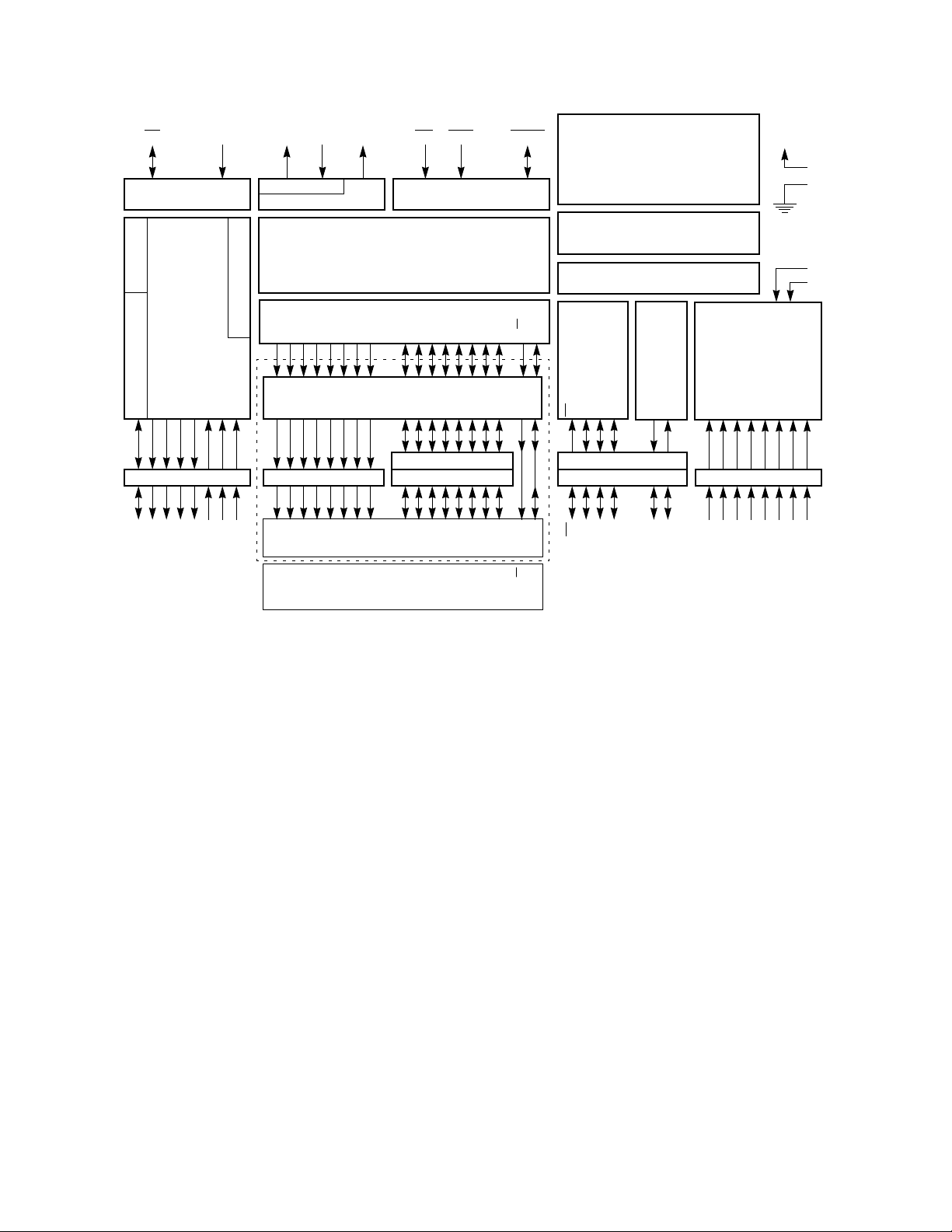
1
Figure 1-1 is a block diagram of the MC68HC11A8 MCU. This diagram shows the ma-
jor subsystems and how they relate to the pins of the MCU. In the lower right-hand corner of this diagram, the parallel I/O subsystem is shown inside a dashed box. The
functions of this subsystem are lost when the MCU is operated in expanded modes,
but the MC68HC24 port replacement unit can be used to regain the functions that were
lost. The functions are restored in such a way that the software programmer is unable
to tell any difference between a single-chip system or an expanded system containing
the MC68HC24. By using an expanded system containing an MC68HC24 and an external EPROM, the user can develop software intended for a single-chip application.
1.2 Programmer’s Model
In addition to executing all M6800 and M6801 instructions, the M68HC11 instruction
set includes 91 new opcodes. The nomenclature M68xx is used in conjunction with a
specific CPU architecture and instruction set as opposed to the MC68HC11xx nomenclature, which is a reference to a specific member of the M68HC11 Family of MCUs.
Figure 1-2 shows the seven CPU registers available to the programmer. The two 8-
bit accumulators (A and B) can be used by some instructions as a single 16-bit accumulator called the D register, which allows a set of 16-bit operations even though the
CPU is technically an 8-bit processor.
The largest group of instructions added involve the Y index register. Twelve bit manipulation instructions that can operate on any memory or register location were added.
The exchange D with X and exchange D with Y instructions can be used to quickly get
index values into the double accumulator (D) where 16-bit arithmetic can be used. Two
16-bit by 16-bit divide instructions are also included.
MOTOROLA
1-2 REFERENCE MANUAL
GENERAL DESCRIPTION
M68HC11
Page 19
MODA/
LIR
COPPULSE ACCUMULATOR
PA7/PAI/OC1
PA6/OC2/OC1
CIRCUITRY ENCLOSED BY DOTTED LINE IS EQUIVALENT TO MC68HC24.
MODB/
V
MODE
CONTROL
TIMER
SYSTEM
PORT A
PA5/OC3/OC1
PA4/OC4/OC1
PA3/OC5/OC1
STBY
OSCILLATOR
PERIODIC INTERRUPT
PA2/IC1
PA1/IC2
PA0/IC3
EXTALXTAL
CLOCK LOGIC
BUS EXPANSION
ADDRESS
STROBE AND HANDSHAKE
PORT B
PB7
PB6
PB5
PB4
PB3
PB2
A15
A14
A13
A12
A11
A10
E
CPU
PARALLEL I/O
PB1
PB0
SINGLE CHIP MODE
A9
EXPANDED MODE
PC7
A8
A7/D7
IRQ/
XIRQ
INTERRUPT LOGIC
ADDRESS/DATA
CONTROL
PORT C
PC6
PC5
PC4
PC3
A6/D6
A5/D5
A4/D4
A3/D3
PC2
PC1
A2/D2
A1/D1
RESET
PC0
A0/D0
R/W
AS
STRA
STRB
AS
R/W
8 KBYTES ROM
512 BYTES EEPROM
256 BYTES RAM
SPI A/D CONVERTERSCI
SS
SCK
MOSI
MISO
CONTROL
PORT D
PD5/SS
PD4/SCK
PD3/MOSI
PD2/MISO
TxD
RxD
PD1/TxD
PD0/RxD
PORT E
PE7/AN7
PE6/AN6
PE5/AN5
PE4/AN4
PE3/AN3
V
V
V
V
PE2/AN2
PE1/AN1
PE0/AN0
DD
SS
RH
RL
1
Figure 1-1 Block Diagram
M68HC11
GENERAL DESCRIPTION
MOTOROLA
REFERENCE MANUAL 1-3
Page 20

1
7070
15 0
AB
D
IX
IY
SP
PC
70
8-BIT ACCUMULATORS A & B
OR 16-BIT DOUBLE ACCUMULATOR D
INDEX REGISTER X
INDEX REGISTER Y
STACK POINTER
PROGRAM COUNTER
CONDITION CODES
CVZNIHXS
CARRY/BORROW FROM MSB
OVERFLOW
ZERO
NEGATIVE
I-INTERRUPT MASK
HALF CARRY (FROM BIT 3)
X-INTERRUPT MASK
STOP DISABLE
Figure 1-2 M68HC11 Programmer’s Model
1.3 Product Derivatives
The M68HC11 Family of MCUs is composed of several members (see Table 1-1 ), and
new members are being developed.
Figure 1-3 explains how the product part num-
bers are constructed.
MOTOROLA
1-4 REFERENCE MANUAL
GENERAL DESCRIPTION
M68HC11
Page 21
QUALIFICATION LEVEL
MC — FULLY SPECIFIED AND QUALIFIED
XC — PILOT PRODUCTION DEVICE
PC — ENGINEERING SAMPLE
NUMERIC DESIGNATOR (OPTIONAL)
OPERATING VOLTAGE RANGE
HC —
HCMOS (V
L —
HCMOS (V
COP OPTION (ONLY ON A-SERIES DEVICES)
NONE —
MEMORY TYPE
BLANK —
BASE PART NUMBER
11A8, 11D3, 11E9, 11K4, ETC.
COP DISABLED
P —
COP ENABLED
MASKED ROM OR NO ROM
7 —
EPROM/OTPROM
8 — EEPROM
= 5.0 VDC ±10%)
DD
= 3.0 VDC TO 5.5 VDC)
DD
MC 68 HC P 11XX B C FN 3 R2
7
1
MONITOR MASK
NONE —
TEMPERATURE RANGE
NONE —
PACKAGE TYPE
FN —
FS —
FU —
FB —
PV —
PU —
PB —
MAXIMUM SPECIFIED CLOCK SPEED
2 —
3 —
4 —
TAPE AND REEL OPTION
NONE —
BLANK
B —
BUFFALO
0°C TO 70°C
C —
– 40°C TO 85°C
V —
– 40°C TO 105°C
M —
– 40°C TO 125°C
44/52/68/84-PIN PLCC
44/52/68/84-PIN CLCC
64/80-PIN QFP
44-PIN QFP
112-PIN TQFP
80/100-PIN TQFP
52-PIN TQFP
P —
40/48-PIN DIP
S —
48-PIN SDIP
2.0 MHz
3.0 MHz
4.0 MHz
STANDARD PACKAGING
R2 —
TAPE AND REEL PACKAGING
HC11 PART NUMBERING
Figure 1-3 Part Numbering
M68HC11
REFERENCE MANUAL 1-5
GENERAL DESCRIPTION
MOTOROLA
Page 22

1
Table 1-1 M68HC11 Family Members
$FF
$FF
2
3
No ROM Part for Expanded Systems
3
High-Performance Non-Multiplexed 6B-Pin
Comments
, 84-Pin
S
Part Number EPROM ROM EEPROM RAM CONFIG
MC68HC11A8 — — 512 256 $0F Family Built Around This Device
MC68HC11A1 — — 512 256 $0D ’A8 with ROM Disabled
MC68HC11A0 — — — 256 $0C ’A8 with ROM and EEPROM Disabled
MC68HC811A8 — — 8K + 512 256 $0F EEPROM Emulator for ’A8
MC68HC11E9 — 12K 512 512 $0F Four Input Capture/Bigger RAM 12K ROM
MC68HC11E1 — — 512 512 $0D ’E9 with ROM Disabled
MC68HC11E0 — — — 512 $0C ’E9 with ROM and EEPROM Disabled
1
MC68HC811E2 — —
MC68HC711E9 12K — 512 512 $0F One-Time Programmable Version of ’E9
MC68HC11D3 — 4K — 192 N/A Low-Cost 40-Pin Version
MC68HC711D9 4K — — 192 N/A One-Time Programmable Version of ’D3
MC68HC11F1 — —
MC68HC11K4 — 24K 640 768 $FF > 1 Mbyte memory space, PWM, C
MC68HC711K4 24K — 640 768 $FF One-Time Programmable Version of ’K4
MC68HC11L6 — 16K 512 512 $0F Like ’E9 with more ROM and more I/O, 64/68
MC68HC711L6 16K — 512 512 $0F One-Time Programmable Version of ’L4
2K
512
256
1
1K
1. The EEPROM is relocatable to the top of any 4 Kbyte memory page. Relocation is done with the upper four bits of
the CONFIG register.
2. CONFIG register values in this table reflect the value programmed prior to shipment from Motorola.
3. At the time of this printing a change was being considered that would make this value $0F.
MOTOROLA
1-6 REFERENCE MANUAL
GENERAL DESCRIPTION
M68HC11
Page 23

SECTION 2 PINS AND CONNECTIONS
This section discusses the functions of each pin on the MC68HC11A8. Most pins on
this microcontroller unit (MCU) serve two or more functions. Information about the
practical use of each pin is presented in these pin descriptions. This section also includes information concerning pins that are exposed to illegal levels or conditions. The
most common source of illegal levels or conditions is transient noise; however, a designer may wish to take precautions against potential misapplication of a product or
failures of other system components such as power supplies. Consideration of these
factors can influence end-product reliability.
The basic connections for single-chip-mode and expanded-mode applications are presented in
panded-Mode-System Connections
starting point for any user application and can minimize the time required to achieve a
working prototype system. The explanation of these basic systems includes information concerning additions, such as additional memory on the expanded system.
2.5 Typical Single-Chip-Mode System Connections and 2.6 Typical Ex-
. These basic systems can be used as the
2
System noise generation and susceptibility primarily depend on each system and its
environment. The MC68HC11A8 is designed for higher bus speeds than earlier
MCUs; since it is high-density complementary metal-oxide semiconductor (HCMOS),
signals drive from rail to rail, unlike earlier N-channel metal-oxide semiconductor
(NMOS) processors. Since these factors can significantly affect noise issues, the system designer should consider these changes.
2.1 Packages And Pin Names
The following figures show pin assignments for several members of the M68HC11
MCU Family. The pin assignments for the MC68HC24 port replacement unit (PRU)
are also presented for reference although the PRU is not discussed in detail in this
manual.
Detailed mechanical data for packages may be found in the data sheets or technical
summaries. Ordering information, which relates part number suffixes to package types
and operating temperature range, are also found in the data sheets or technical summaries.
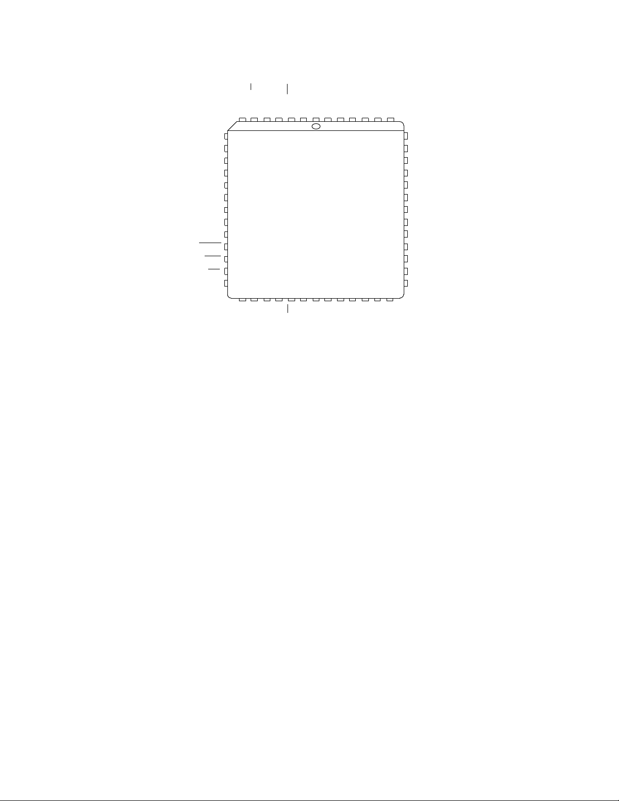
2.1.1 MC68HC11A8
The MC68HC11A8 is available in either a 52-pin plastic leaded chip carrier (PLCC)
package or a 48-pin dual-in-line package (DIP). The silicon die is identical for both
packages, but four of the analog-to-digital (A/D) converter inputs are not bonded out
to pins in the 48-pin DIP. The MC68HC11A1 and MC68HC11A0 devices also use the
same die as the MC68HC11A8, except that the contents of the nonvolatile CONFIG
register determine whether or not internal read-only memory (ROM) and/or electrically
erasable programmable ROM (EEPROM) are disabled. These downgraded device
versions have identical pin assignments as the MC68HC11A8.
M68HC11
REFERENCE MANUAL 2-1
PINS AND CONNECTIONS
MOTOROLA
Page 24
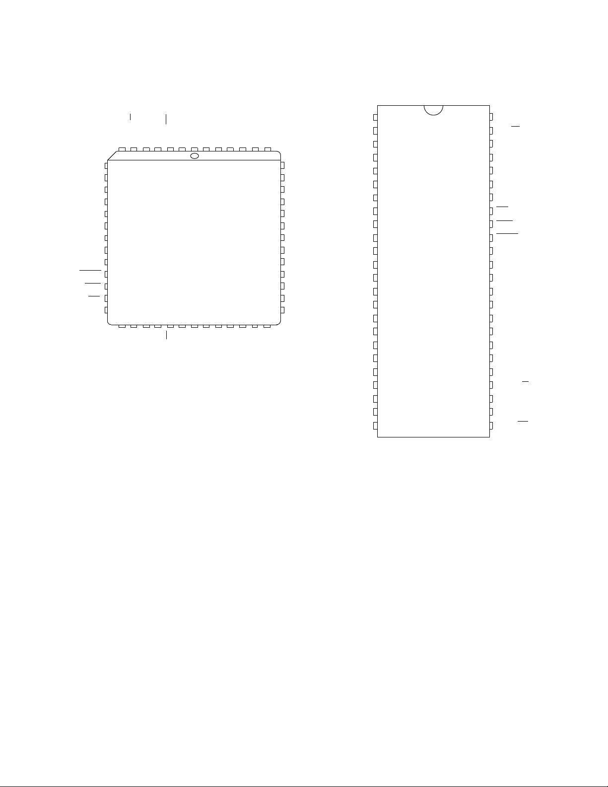
Figure 2-1 shows the pin assignments for the MC68HC11A8 in the 52-pin PLCC pack-
age and the 48-pin DIP package.
2
XTAL
PC0/A0/D0
PC1/A1/D1
PC2/A2/D2
PC3/A3/D3
PC4/A4/D4
PC5/A5/D5
PC6/A6/D6
PC7/A7/D7
RESET
XIRQ
IRQ
PD0/RxD
STBY
MODB/V
EXTAL
STRB/R/WESTRA/AS
765
8
9
10
11
12
13
14
15
16
17
18
19
20
2122232425262728293031
PD1/TxD
PD2/MISO
PD3/MOSI
4
PD4/SCK
VSSVRHV
MODA/LIR
312
525150
MC68HC11A8
DD
V
PD5/SS
PA7/PAI/OC1
PA6/OC2/OC1
RL
PE7/AN7
PE3/AN3
49
PA5/OC3/OC1
PA4/OC4/OC1
PA3/OC5/OC1
PE6/AN648
PE2/AN2
47
46
45
44
43
42
41
40
39
38
37
36
35
34
33
PA2/IC132PA1/IC2
PE5/AN5
PE1/AN1
PE4/AN4
PE0/AN0
PB0/A8
PB1/A9
PB2/A10
PB3/A11
PB4/A12
PB5/A13
PB6/A14
PB7/A15
PA0/IC3
PA7/PAI/OC1
PA6/OC2/OC1
PA5/OC3/OC1
PA4/OC4/OC1
PA3/OC5/OC1
PA2/IC1
PA1/IC2
PA0/IC3
PB7/A15
PB6/A14
PB5/A13
PB4/A12
PB3/A11
PB2/A10
PB1/A9
PB0/A8
PE0/AN0
PE1/AN1
PE2/AN2
PE3/AN3
V
V
RH
V
SS
MODB/V
STBY
V
1
2
3
4
5
6
7
8
9
10
11
12
13
14
15
16
17
18
19
20
21
RL
22
23
24
MC68HC11A8
48
47
46
45
44
43
42
41
40
39
38
37
36
35
34
33
32
31
30
29
28
27
26
25
DD
PD5/SS
PD4/SCK
PD3/MOSI
PD2/MISO
PD1/TxD
PD0/RxD
IRQ
XIRQ
RESET
PC7/A7/D7
PC6/A6/D6
PC5/A5/D5
PC4/A4/D4
PC3/A3/D3
PC2/A2/D2
PC1/A1/D1
PC0/A0/D0
XTAL
EXTAL
STRB/R/W
E
STRA/AS
MODA/LIR
Figure 2-1 MC68HC11A8 Pin Assignments
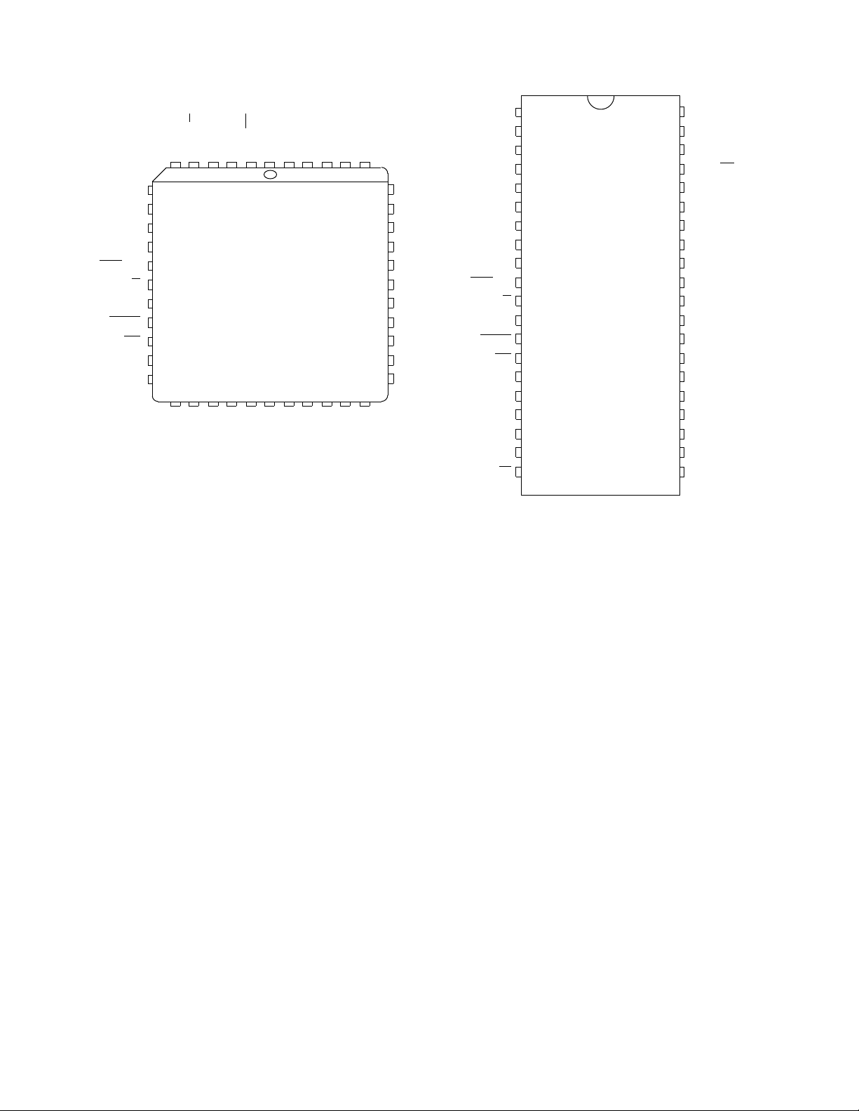
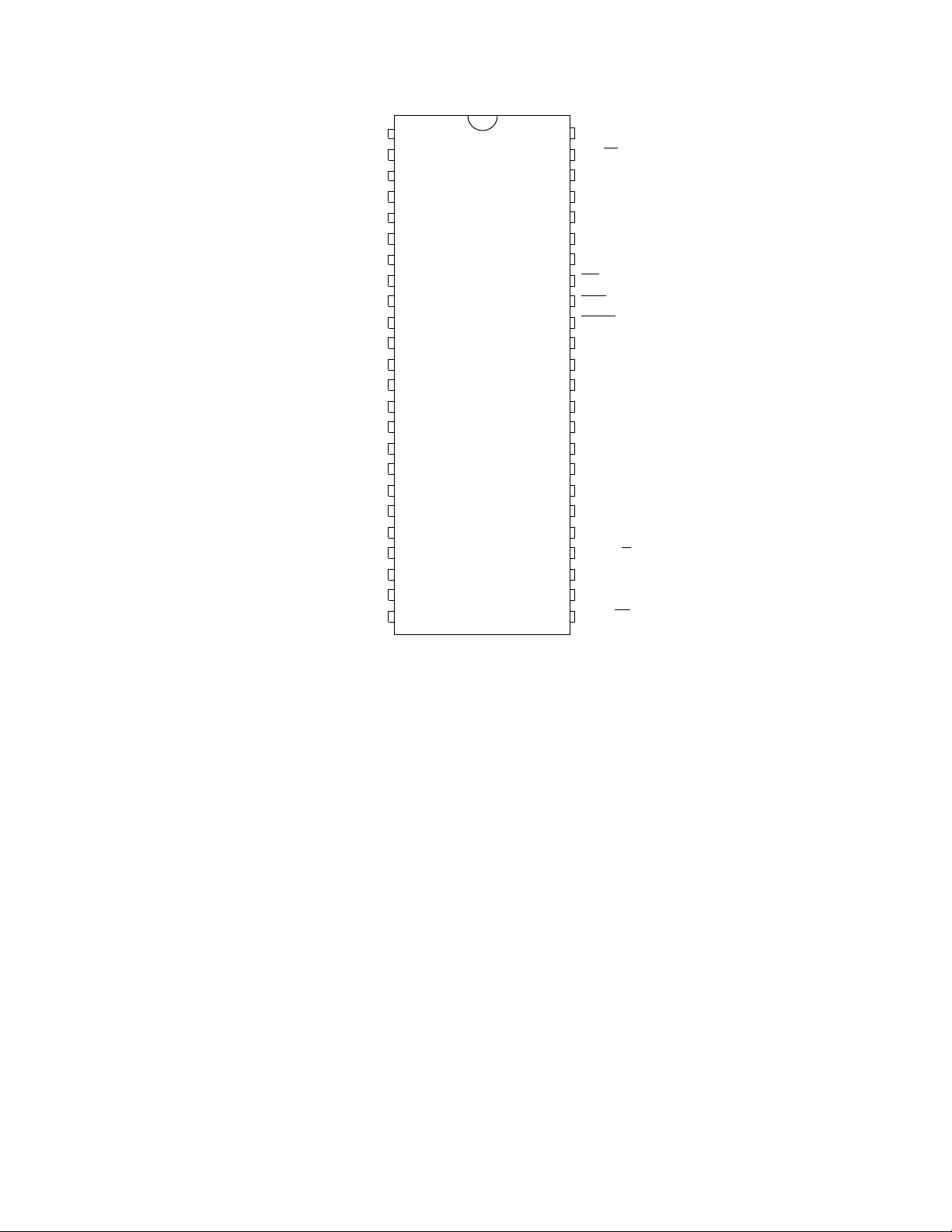
2.1.2 MC68HC11D3/711D3
The MC68HC11D3 is available in either a 44-pin PLCC package or a 40-pin DIP package. The silicon die is identical for both packages, but the PLCC version has two additional output compare pins bonded out and an extra V
pin named E
SS
VSS
. The
MC68HC711D3 is functionally equivalent to the MC68HC11D3 but has 4 Kbytes of
EPROM instead of mask programmed ROM. The MC68HC711D3 is available as a
one-time-programmable (OTP) MCU in an opaque plastic package or in a ceramic
windowed package for development applications.
Figure 2-2 shows the pin assignments for the MC68HC11D3/711D3 in the 44-pin
PLCC package and the 40-pin DIP package.
MOTOROLA
2-2 REFERENCE MANUAL
PINS AND CONNECTIONS
M68HC11
Page 25
PC4/ADDR4
PC5/ADDR5
PC6/ADDR6
PC7/ADDR7
XIRQ/V
PD7/R/W
PD6/AS
RESET
IRQ
PD0/RxD
PD1/TxD
V
1
STBY
EXTAL
STRB/R/WESTRA/AS
6
5
7
8
9
10
11
PP
12
13
14
15
16
17
1819202122
PD2/MISO
PD3/MOSI
MODA/LIR
4
3
2
MC68HC(7)11D3
DD
V
PD4/SCK
PA7/PAI/OC1
MODB/V
VSSVRHVRLPE7/AN7
44
434241
1
2324252627
PA6/OC3/OC1
PA5/OC3/OC1
PA5/OC3/OC1
PA4/OC4/OC1
PE3/AN3
40
39
PB0/ADDR8
PB1/ADDR9
38
37
PB2/ADDR10
36
PB3/ADDR11
35
PB4/ADDR12
PB5/ADDR13
34
33
PB6/ADDR14
PB7/ADDR15
32
NC
31
30
PA0/IC3
29
PA1/IC2
28
PA2/IC1
PA3/IC4/OC5/OC1
PC0/ADDR0
PC1/ADDR1
PC2/ADDR2
PC3/ADDR3
PC4/ADDR4
PC5/ADDR5
PC6/ADDR6
PC7/ADDR7
XIRQ
/V
PD7/R/W
PD6/AS
RESET
IRQ
PD0/RxD
PD1/TxD
PD2/MISO
PD3/MOSI
PD4/SCK
PD5/SS
SS
2
3
4
5
6
7
MC68HC(7)11D3
8
9
PP
10
11
12
13
14
15
16
17
18
19
20
XTAL
40
EXTAL
39
E
38
MODA/LIR
37
MODB/V
36
PB0/ADDR8
35
PB1/ADDR9
34
PB2/ADDR10
33
PB4/ADDR12
32
PB5/ADDR13
31
PB6/ADDR14
30
PB7/ADDR15
29
PA0/IC3
28
PA1/IC2
27
PA1/IC2
26
PA2/IC1
25
PA3/IC4/OC5/OC1
24
PA5/OC3/OC1
23
PA7/PAI/OC1
22
V
21
DD
STBY
2
Figure 2-2 MC68HC11D3/711D3 Pin Assignments
2.1.3 MC68HC11E9/711E9
The MC68HC11E9 is available in a 52-pin PLCC package only. The MC68HC11E1
and MC68HC11E0 devices also use the same die as the MC68HC11E9, except that
the contents of the nonvolatile CONFIG register determine whether or not internal
ROM and/or EEPROM are disabled. These downgraded device versions have identical pin assignments as the MC68HC11E9.
The MC68HC11E9 is an upgrade of the MC68HC11A8. The MC68HC11E9 has 12
Kbytes of mask ROM, 512 bytes of EEPROM, and 512 bytes of RAM. The timer system allows one output-compare channel to be reconfigured as a fourth input-capture
channel.
The MC68HC711E9 is functionally equivalent to the MC68HC11E9 but has 12 Kbytes
of EPROM instead of mask programmed ROM. The MC68HC711E9 is available as a
one-time programmable (OTP) MCU in an opaque plastic package or in a ceramic windowed package for development applications.
Figure 2-3 shows the pin assignments for the MC68HC11E9 in the 52-pin PLCC pack-
ages. These pin assignments are the same as the MC68HC11A8, except for the pin
name for the PA3/OC5/IC4/OC1 pin.
M68HC11
PINS AND CONNECTIONS
MOTOROLA
REFERENCE MANUAL 2-3
Page 26
STBY
2
RL
VSSVRHV
525150
PA7/PAI/OC1
PA6/OC2/OC1
PA5/OC3/OC1
PE7/AN7
PE3/AN3
PE6/AN648
49
PA2/IC132PA1/IC2
PA4/OC4/OC1
PA3/OC5/OC1
PE2/AN2
47
46
45
44
43
42
41
40
39
38
37
36
35
34
33
PE5/AN5
PE1/AN1
PE4/AN4
PE0/AN0
PB0/A8
PB1/A9
PB2/A10
PB3/A11
PB4/A12
PB5/A13
PB6/A14
PB7/A15
PA0/IC3
XTAL
PC0/A0/D0
PC1/A1/D1
PC2/A2/D2
PC3/A3/D3
PC4/A4/D4
PC5/A5/D5
PC6/A6/D6
PC7/A7/D7
RESET
XIRQ
IRQ
PD0/RxD
EXTAL
STRB/R/WESTRA/AS
765
8
9
10
11
12
13
14
15
16
17
18
19
20
2122232425262728293031
PD1/TxD
PD2/MISO
PD3/MOSI
MODB/V
MODA/LIR
4
312
MC68HC11E9
DD
V
PD5/SS
PD4/SCK
Figure 2-3 MC68HC11E9/711E9 Pin Assignments (52-Pin PLCC)
2.1.4 MC68HC811E2
The MC68HC811E2 is very similar to the MC68HC11E9 version, except in the on-chip
memory. The MC68HC811E2 includes 2 Kbytes of EEPROM, which can be remapped
to the upper half of any 4 Kbyte page in the 64 Kbyte map. There is no masked ROM
memory in the MC68HC811E2. The MC68HC811E2 is available in either a 52-pin
PLCC package or a 48-pin DIP. The silicon die used is the same for both packages,
but four of the A/D converter inputs are not bonded out to pins in the 48-pin package.
The MC68HC811E2 version replaces an earlier version called the MC68HC811A2.
The only significant difference between the MC68HC811E2 and MC68HC811A2 is
that the MC68HC811E2 has a slightly more flexible timer system, which allows one
output-compare channel to be reconfigured as a fourth input-capture channel.
The 52-pin PLCC package version of the MC68HC811E2 has identical pin assignments to the MC68HC11E9 pin assignments shown in
Figure 2-3 . Figure 2-4 illus-
trates the pin assignments for the MC68HC811E2 in the 48-pin DIP.
MOTOROLA
PINS AND CONNECTIONS
M68HC11
2-4 REFERENCE MANUAL
Page 27
PA7/PAI/OC1
PA6/OC2/OC1
PA5/OC3/OC1
PA4/OC4/OC1
PA3/OC5/OC1
PA2/IC1
PA1/IC2
PA0/IC3
PB7/A15
PB6/A14
PB5/A13
PB4/A12
PB3/A11
PB2/A10
PB1/A9
PB0/A8
PE0/AN0
PE1/AN1
PE2/AN2
PE3/AN3
V
RL
V
RH
V
SS
MODB/V
STBY
1
2
3
4
5
6
7
8
9
10
11
12
13
14
15
16
17
18
19
20
21
22
23
24
MC68HC811E2
48
47
46
45
44
43
42
41
40
39
38
37
36
35
34
33
32
31
30
29
28
27
26
25
V
DD
PD5/SS
PD4/SCK
PD3/MOSI
PD2/MISO
PD1/TxD
PD0/RxD
IRQ
XIRQ
RESET
PC7/A7/D7
PC6/A6/D6
PC5/A5/D5
PC4/A4/D4
PC3/A3/D3
PC2/A2/D2
PC1/A1/D1
PC0/A0/D0
XTAL
EXTAL
STRB/R/W
E
STRA/AS
MODA/LIR
2
Figure 2-4 MC68HC811E2 Pin Assignments (48-Pin DIP)
2.1.5 MC68HC11F1
The MC68HC11F1 is available in a 68-pin PLCC package only. The MC68HC11F1 is
the first non-multiplexed address/data bus version of the M68HC11 family. In addition
to the non-multiplexed bus, this MCU includes 1 Kbyte of on-chip RAM and intelligent
chip selects for simple connection to external program memory without the need for
any external logic chips. Other on-chip peripherals are similar to the MC68HC11E9.
Figure 2-5 shows the pin assignments for the MC68HC11F1 in the 68-pin PLCC pack-
age.
M68HC11
PINS AND CONNECTIONS
MOTOROLA
REFERENCE MANUAL 2-5
Page 28

STBY
2
DATA1/PC1
DATA2/PC2
DATA3/PC3
DATA4/PC4
DATA5/PC5
DATA6/PC6
DATA7/PC7
RESET
XIRQ
IRQ
CSPROG/PG7
CSGEN/PG6
CSIO1/PG5
CSIO2/PG4
PG3
PG2
PG1
10
11
12
13
14
15
16
17
18
19
20
21
22
23
24
25
26
DATA0/PC0
4XOUT
9
8
7
27
28
PG0
RxD/PD0
XTAL
EXTAL
6
514
293031
TxD/PD1
MISO/PD2
R/W
E
MODA/LIR
3
MC68HC11F1
3233343536
SS/PD5
SCK/PD4
MOSI/PD3
VSSVRHV
MODB/V
2
DD
V
PAI/OC1/PA7
RL
PE7/AN766
68
67
37
OC2/OC1/PA6
OC3/OC1/PA5
OC4/OC1/PA4 38
PE3/AN3
PE6/AN6
PE2/AN2
64
63
65
40
41
39
IC1/PA2
IC2/PA1
OC5/OC1/PA3
PE5/AN562
PE1/AN2
61
60
59
58
57
56
55
54
53
52
51
50
49
48
47
46
45
44
43
IC3/PA0 42
ADDR15/PB7
PE4/AN4
PE0/AN0
PF0/ADDR0
PF1/ADDR1
PF2/ADDR2
PF3/ADDR3
PF4/ADDR4
PF5/ADDR5
PF6/ADDR6
PF7/ADDR7
PB0/ADDR8
PB1/ADDR9
PB2/ADDR10
PB3/ADDR11
PB4/ADDR12
PB5/ADDR13
PB6/ADDR14
Figure 2-5 MC68HC11F1 Pin Assignments (68-Pin PLCC)
2.1.6 MC68HC24 Port Replacement Unit
The MC68HC24 is available in either a 44-pin PLCC package or a 40-pin DIP. Figure
shows the pin assignments for the MC68HC24 in the 44-pin PLCC package and
2-6
the 40-pin DIP package.
MOTOROLA
2-6 REFERENCE MANUAL
PINS AND CONNECTIONS
M68HC11
Page 29
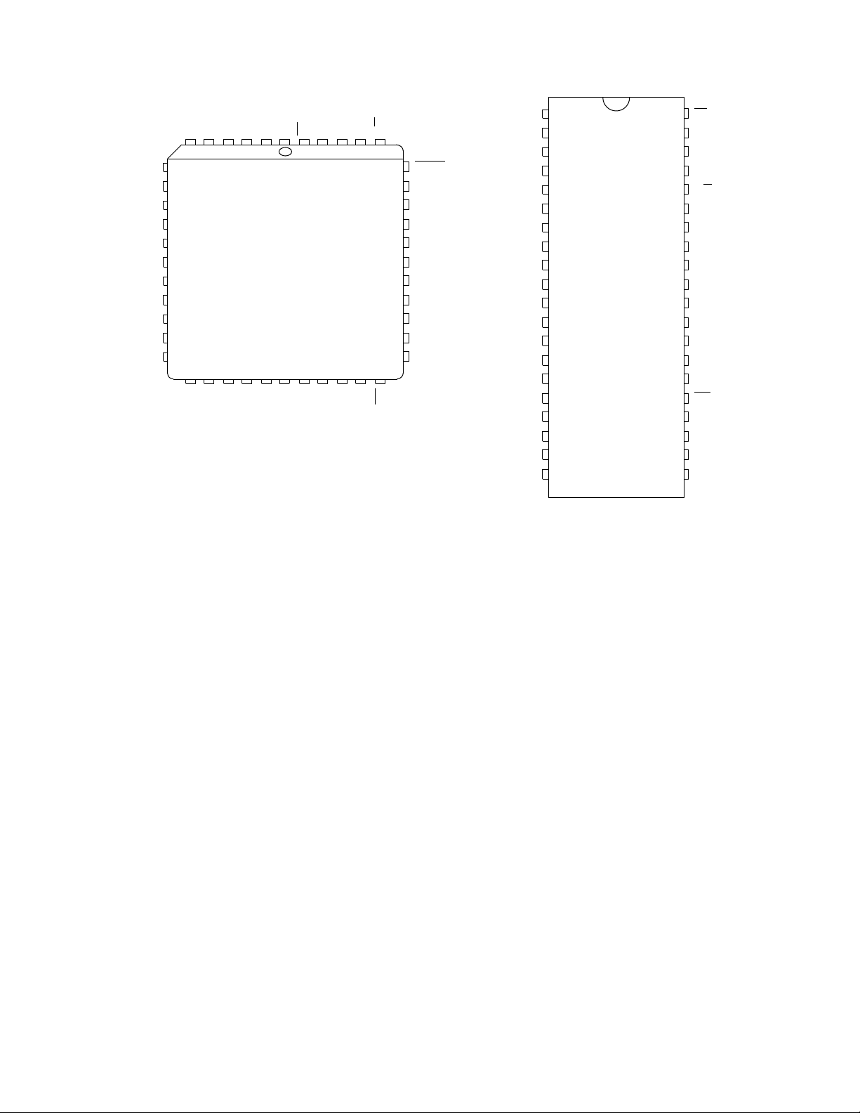
)
STRA
PC0
PC1
PC2
PC3
NC
PC4
PC5
PC6
PC7
V
I/O TEST
A12
A13
A14
A15
I/O TESTNCCS
6
5
4
3
2
7
8
9
10
11
12
13
14
15
16
17
DD
18
STRB
19
PB7
MC68HC24
202122
PB6
PB5
PB4NCPB3
MODEASE
44
434241
1
2324252627
PB2
PB1
PB0
R/W
40
28
IRQ
39
RESET
AD0
38
37
AD1
36
AD2
35
AD3
NC
34
33
AD4
AD5
32
AD6
31
30
AD7
29
V
SS
A15
A14
A13
A12
STRA
PC0
PC1
PC2
PC3
PC4
PC5
PC6
PC7
V
STRB
PB7
PB6
PB5
PB4
1
2
3
4
5
6
7
MC68HC24
8
9
10
11
12
13
14
15
DD
16
17
18
19
20
CS
40
MODE
39
AS
38
E
37
R/W
36
RESET
35
AD0
34
AD1
33
AD2
32
AD3
31
AD4
30
AD5
29
AD6
28
AD7
27
V
26
SS
IRQ
25
PB0
24
PB1
23
PB2
22
PB3
21
2
Figure 2-6 MC68HC24 Pin Assignments
2.2 Pin Descriptions
This section provides a pin-by-pin description of the MCU. In general, a designer
should consider all possible functions of each pin when designing the MCU into an application system.
schematics of the logic associated with each of the I/O pins.
RATION AND MODES OF OPERATION
SECTION 7 PARALLEL INPUT/OUTPUT contains transistor-level
SECTION 3 CONFIGU-
discusses the pins that operate as a multiplexed address/data bus in expanded modes of operation as well as the functions of
other pins related to mode selection and bus control. The reset and interrupt pins are
presented again in
SECTION 5 RESETS AND INTERRUPTS . Sections 8 through 12
discuss pins related to the on-chip peripherals presented in those sections.
Figure 1-1 is a pin-function-oriented block diagram of the MC68HC11A8, which is a
good reference for development and verification of application designs.
2.2.1 Power-Supply Pins (V
Power is supplied to the MCU by using these pins. V
is ground. The MC68HC11A8 MCU uses a single power supply, but in some ap-
V
SS
and V
DD
SS
is the positive power input, and
DD
plications, there may also be optional power supplies for A/D reference and/or for battery backup of on-chip random-access memory (RAM). These additional power
sources are optional, and the MCU, including RAM and A/D, can operate from a single
5-V (nominal) power supply.
M68HC11
PINS AND CONNECTIONS
MOTOROLA
REFERENCE MANUAL 2-7
Page 30

2
µ
µ
µ
µ
µ
Although the MC68HC11A8 is a CMOS device, very fast signal transitions are present
on many of the pins. Even when the MCU is operating at slow clock rates, short rise
and fall times are present. Depending upon the loading on these fast signals, significant short-duration current demands can be placed on the MCU power supply. Special
care must be taken to provide good power-supply bypassing at the MCU.
The faster edge times in the MC68HC11A8 generally place greater demands on bypassing than earlier NMOS MCU designs. A typical expanded-mode system should include a 1be as close (physically and electrically) as possible to the MC68HC11A8 and should
have good high-frequency characteristics (i.e., not old-technology dipped ceramic
disc). The 1low-impedance path (minimum-length runners). Without this bypass, there could be
very large voltage drops in the circuit board runners to the MCU due to the very high
(although very short duration) current spike caused by several MCU pins simultaneously switching from one level to the other. The separate 0.01cluded because the larger 1high-frequency (low energy) noise. These are only general recommendations. Some
lightly loaded single-chip systems may work quite well with a single 0.1pacitor; whereas, more heavily loaded expanded-mode systems may require more
elaborate bypassing measures.
F capacitor and a separate 0.01- µ F capacitor. Both these capacitors should
F capacitor primarily supplies charge for bus switching through a very
F capacitor is in-
F capacitor is typically not as good at snubbing very
F bypass ca-
It is easier and less expensive to approach power-supply layout and bypassing as a
preventive measure from the beginning of a design than to locate and correct a noise
problem in a marginal design. Problems related to inadequate power-supply layout
and bypassing are very difficult to locate and correct, but, if reasonable care is taken
from the start of a design, noise should not arise as a problem.
2.2.2 Mode Select Pins (MODB/V
The mode B/standby RAM supply (MODB/V
input pin and a standby power-supply pin. The mode A/load instruction register (MODA/LIR
it operates as a diagnostic output signal while the MCU is executing instructions.
The hardware mode select mechanism starts with the logic levels on the MODA and
MODB pins while the MCU is in the reset state. The logic levels on the MODA and
MODB pins are fed into the MCU via a clocked pipeline path. The levels captured are
those that were present part of a clock cycle before the RESET
sures there will be a zero hold-time requirement on the mode select pins relative to the
rising edge at the RESET pin. The captured levels determine the logic state of the special mode (SMOD) and mode A select (MDA) control bits in the highest priority interrupt (HPRIO) register. These two control bits actually control the logic circuits involved
in hardware mode selection. Mode A selects between single-chip modes and expanded modes; mode B selects between the normal variation and the special variation of
the chosen operating mode. Bootstrap mode is the special variation of single-chip
mode, and special test is the special variation of expanded mode.
rizes the operation of the mode pins and mode control bits.
) pin is used to select the MCU operating mode while the MCU is in reset, and
and MODA/LIR )
STBY
) pin functions as both a mode select
STBY
pin rose, which as-
Table 2-1 summa-
MOTOROLA
2-8 REFERENCE MANUAL
PINS AND CONNECTIONS
M68HC11
Page 31

Table 2-1 Hardware Mode Select Summary
Inputs
MODB MODA RBOOT SMOD MDA IRV
1 0 Normal Single Chip 0000
1 1 Normal Expanded 0010
0 0 Special Bootstrap 1101
0 1 Special Test 0111
After reset is released, the mode select pins no longer influence the MCU operating
mode. The MODA pin serves the alternate function of load instruction register (LIR
when the MCU is not in reset. The open-drain active-low LIR
ing the first E cycle of each instruction. The MODB pin serves the alternate function of
a standby power supply (V
The power-saving mode, STOP, is an alternate way to save RAM contents, which
does not require a separate standby power source.
The LIR
tem. Since this status indicator shows where each instruction begins, programs can
be followed easily. The mode A select levels and the LIR
to prevent interference between the shared functions of the pin. In single-chip applications, this pin is simply connected to V
no conflict between the direct V
during the first E cycle of each instruction. There is no practical reason to monitor LIR
during single-chip modes because there is no visibility to internal data and address
buses. In expanded-mode systems, the MODA/LIR
a 4.7 kΩ resistor. During reset, the pull-up resistor instructs the MODA pin to select
expanded modes. During-program execution, the pin is driven low during the first cycle
of each instruction by the LIR
ternal 4.7 kΩ pull-up.
function is intended for monitoring on a logic analyzer during debug of a sys-
Mode Description
) to maintain RAM contents when VDD is not present.
STBY
connection and the LIR signal that drives the pin low
SS
signal and is pulled up between LIR signals by the ex-
SS
Control Bits in HPRIO (Latched at Reset)
output pin drives low dur-
status levels were selected
. Since the LIR output is open-drain, there is
pin is normally pulled up to VDD by
)
2
In expanded-mode systems where it is important to minimize power-supply current,
logic could be used to drive the MODA/LIR
(see Figure 2-7). During reset, the MODA pin would be driven high to select expanded
mode. After reset, the LIR
operating against a pull-up, but rather it should be a logic-gate-type output with some
series resistance to protect against the unlikely event of a conflict between an activelow LIR
occur briefly at the falling edge of reset. Since LIR
three cycles during normal execution (average instructions take about three cycles),
I
DD
M68HC11
REFERENCE MANUAL 2-9
signal and an active-high logic-gate output signal. Such a conflict could only
could be reduced by about 350 µA (5 V ÷ 4.7 kΩ x 33% duty cycle).
RESET
Figure 2-7 Reduced IDD MODA/LIR Connections
pin would be driven low by logic. The logic should not be
74HC04
PINS AND CONNECTIONS
pin rather than just using a simple pull-up
is active for about one out of every
4.7K
TO MODA/LIR
OF M68HC11
MOTOROLA
Page 32

2
The V
or VDD to the RAM and reset logic, depending upon the relative levels of V
. The switch connects VDD unless V
V
DD
function is accomplished by a transistor switch that connects either V
STBY
is more than a threshold higher than VDD.
STBY
STBY
STBY
and
A threshold is approximately a diode drop (0.7 V) but varies from lot to lot due to processing variations. During normal operation of the MCU, V
RAM. In a standby situation, V
should be maintained at a valid level, and RESET
STBY
is supplying power to the
DD
should be activated (pulled low) when VDD drops below legal limits. RESET should always be held low whenever V
ated in a special mode (MODB low before applying reset) and the MODB/V
being used to back up the RAM, the MODB/V
is at (has returned to) a legal level. Some logic may be required in systems that
V
DD
use MODB/V
as a standby supply and wish to use one of the special modes of
STBY
operation. In most applications, the MODB pin would be connected to V
is below its operating limit. If the MCU is to be oper-
DD
STBY
pin should not be driven low unless
STBY
through a
DD
pin is
4.7 kΩ pull-up resistor for normal modes or directly to ground for special modes.
There are two ways to maintain the contents of on-chip RAM with minimal power con-
sumption (as in a battery-based application). The preferred method uses the STOP
mode of operation, and the second method uses the MODB/V
pin (see Figure 2-
STBY
8). Each of these methods has advantages. The STOP method is preferred because
it is much simpler than the separate power-supply method in terms of hardware costs
and complexity. The STOP method saves power by stopping all MCU clocks, which
reduces the V
current to a few microamps. No external logic is needed, and the con-
DD
tents of internal registers are maintained in addition to the contents of internal RAM.
The MODB/V
amount of external circuitry operating from V
pin method would be used in cases where there is a significant
STBY
so that the added complexity of two
DD
supplies and added logic is justified by the power savings.
V
DD
4.8 V
NiCd
+
Figure 2-8 RAM Standby MODB/V
V
DD
V
BATT
MAX
690
V
OUT
4.7K
TO MODB/V
OF M68HC11
Connections
STBY
STBY
2.2.3 Crystal Oscillator and Clock Pins (EXTAL, XTAL, and E)
The oscillator pins can be used with an external crystal network or an externally generated CMOS-compatible clock source. The frequency applied to these pins is four
times higher than the desired bus frequency (E-clock rate). The E clock is the bus fre-
MOTOROLA PINS AND CONNECTIONS M68HC11
2-10 REFERENCE MANUAL
Page 33

quency clock output, which is used as a basic timing reference signal. When the E
clock is low (address portion of a bus cycle), an internal process is occurring; when E
is high, data is being addressed. The E clock is free running at one-fourth the crystal
frequency as long as the oscillator is active (STOP stops all clocks).
The oscillator in the MC68HC11A8 consists of a large two-input NAND gate. One of
the inputs to this gate is driven by an internal signal that disables the oscillator when
the MCU is in the STOP mode. The other input is the EXTAL input pin of the MCU.
The output of this NAND gate is the XTAL output pin of the MCU.
The XTAL pin is normally left unterminated when using an external CMOS-compatible
clock input to the EXTAL pin. However, a 10 kΩ-100 kΩ load resistor to ground may
be used to reduce generated radio frequency interference (RFI) noise emission. The
XTAL output is normally intended to drive only a crystal, but XTAL can be used as a 4
x clock output if special care is taken to avoid undesirable loading. The XTAL output
may be buffered with a high-impedance buffer such as the 74HC04, or it may be used
to drive the EXTAL input of another M68HC11 MCU. In all cases, the circuit-board layout around the oscillator pins is critical. Load capacitances specified in the data sheets
and technical summary include all stray layout capacitances. Thus, the physical capacitors connected to these pins should always be less than the specified load capacitances by the estimated interconnection capacitances.
2
Figure 2-9 and Figure 2-10 show the internal and external components that form the
crystal oscillator, called a Pierce oscillator (also known as a parallel resonant crystal
oscillator).
Figure 2-9 shows the connections for high-frequency crystals (greater than 1 MHz),
and Figure 2-10 shows connections for low-frequency operation (less than 1 MHz).
The resistor, R
linear region. In low-frequency designs, R
the power into the crystal, which is important for many small crystals because they are
designed for very low drive levels (typically 1-µW maximum). In high-frequency applications (see Figure 2-9), the output impedance of the NAND driver, combined with the
lower impedance of C1 and C2, provides the same effect as the R
designs. Higher frequency AT-cut crystals are designed for much higher drive levels.
, provides a direct current bias to the input so the NAND operates in its
f
and C2 provide a phase shift. RS also limits
S
in low-frequency
S
M68HC11 PINS AND CONNECTIONS MOTOROLA
REFERENCE MANUAL 2-11
Page 34

2
STOP
M68HC11
XTALEXTAL
R
f
XTAL
C2C1
Figure 2-9 High-Frequency Crystal Connections
STOP
M68HC11
XTALEXTAL
R
f
R
XTAL
S
C2C1
Figure 2-10 Low-Frequency Crystal Connections
Exact values for the external components are a function of wafer processing parameters, package capacitance, printed circuit board (PCB) capacitance and inductance,
socket capacitance, operating voltage, crystal technology, and frequency. Typical values are as follows:
MOTOROLA PINS AND CONNECTIONS M68HC11
2-12 REFERENCE MANUAL
Page 35

Rf = 1 MΩ–20 MΩ Higher values are sensitive to humidity; lower values
reduce gain and could prevent startup.
Cl = 5 pF–25 pF Value is usually fixed.
C2 = 5 pF–25 pF Value may be varied to trim frequency.
A tune-up procedure for experimentally determining RS will be discussed at the conclusion of this subsection. Since circuit and layout capacitances effectively add to the
values of C1 and C2, the physical capacitances are usually smaller than the intended
capacitances.
In most high-frequency applications, the values of C1 and C2 are equal. In low-frequency designs, it is often desirable to make C1 smaller than C2, which provides a
higher voltage at the EXTAL input due to an impedance transformation. The wider voltage swing at this input will result in lower power-supply current.
As in all crystal oscillator designs, all leads should be kept as short as possible. It is
also good practice to route V
the oscillator input from the output and the oscillator from adjacent circuitry, only adding capacitance in parallel with C1 and C2. Potentially noisy lines should be kept as
far as possible from the oscillator components. Ground loops should be avoided
around oscillator components (note the unterminated V
C2 in Figure 2-11).
paths as shown in Figure 2-11. These paths isolate
SS
paths ending under C1 and
SS
2
CRYSTAL
C1C2
PIN 7
R
f
PIN 8
XTAL
Figure 2-11 Crystal Layout Example
EXTAL
M68HC11
MCU
M68HC11 PINS AND CONNECTIONS MOTOROLA
REFERENCE MANUAL 2-13
Page 36

2
Usually, the operation of the oscillator cannot be observed with an oscilloscope connected to one of the oscillator pins. The oscilloscope adds from 3 to 30 pF and from 1
to 10 MΩ to V
is connected to the EXTAL input, the 10 MΩ to V
tive divider with R
ear region of the EXTAL input. This problem can sometimes be overcome by
capacitively coupling the oscilloscope with a very small capacitor (1–5 pF) between
the oscilloscope probe and the oscillator pin. It is usually better to observe the E-clock
output from the MCU since this does not alter the operation of the oscillator.
In low-frequency designs, it is often possible to observe the XTAL node with an oscilloscope because the high-impedance nodes of the oscillator are isolated from XTAL
by R
scope connected. If the I
was unaffected.
Low-frequency crystal circuits tend to be very high impedance. Thus, the PCB must
be clean, dry, and free of conductive material such as solder rosin and excessive moisture from high humidity. If problems occur, the value of R
taminant impedance is less significant in comparison. Of course, it is still best to
eliminate the contaminants.
. Observe IDD without the oscilloscope connected and again with the oscillo-
S
, which will usually affect oscillator operation. When the oscilloscope
SS
(oscilloscope input) forms a resis-
SS
and often disables the oscillator by biasing the circuit out of the lin-
f
is unchanged, it is usually safe to assume the oscillator
DD
can be reduced so the con-
f
Usually, startup time is inversely proportional to the frequency; thus, low-frequency oscillators start slower than high-frequency oscillators. There are many exceptions to this
rule because there are many variables affecting startup time. Observation of a few circuits using the MC68HC11A8 with an 8-MHz crystal reveals startup from STOP takes
approximately two milliseconds, and startup from power-up occurs within a few milliseconds of when V
greatly since power-source turn-on characteristics vary greatly. Since the
MC68HC11A8 is a fully static design, the oscillator is not required to be running full
speed before the processor starts executing instructions (most applications do not require a stable oscillator within the first few milliseconds after power-up). If the oscillator
is not running at full speed, instructions will take longer to execute, but no unpredictable behavior will result as it would in an NMOS processor. An oscillator in the 32-kHz
range could require hundreds of milliseconds or even a few seconds to start and stabilize.
The following tune-up procedure is only meaningful for crystal frequencies below 1 MHz. In higher frequency applications, because R
is normally 0 Ω, this procedure is not needed.
The value of RS can be determined experimentally by using the final PCB and an MCU
of the exact type that will be used in the final application. The MCU need not have the
final mask program because the MCU will be held in reset throughout the experiment.
Because of the number of variables involved, use components with the exact properties of those that will be used in production. For example, do not use a ceramic-packaged MCU prototype for the experiment when a plastic-packaged MCU will be used in
reaches approximately one Volt. Power-up performance varies
DD
NOTE
S
MOTOROLA PINS AND CONNECTIONS M68HC11
2-14 REFERENCE MANUAL
Page 37

production. An emulator version of the part will also have slightly different electrical
properties than the masked ROM version of the same part.
To determine the optimum value for R
MCU as a function of R
because operating current variations during run modes are much greater than the current variations due to varying R
sharp as in many LC circuits but is instead very broad. As the shape of this curve suggests, the exact value of R
Finally, verify that the maximum-operating supply voltage does not overdrive the crystal. Observe the output frequency as a function of V
Under proper operating conditions, the frequency should increase a few parts per million as supply voltage increases. If the crystal is overdriven, an increase in supply voltage will cause a decrease in frequency, or the frequency will become unstable. If
frequency problems arise, supply voltage must be decreased, or the values of R
and C2 should be increased to reduce the crystal drive.
2.2.4 Crystal Oscillator Application Information
Some crystal oscillator application information is presented in the following paragraphs.
2.2.4.1 Crystals for Parallel Resonance
Parallel resonance refers to a Pierce oscillator that has the crystal in parallel with an
inverter. Almost all (if not all) CMOS MCUs use this type oscillator. AT-cut crystals are
available as standard devices for both series resonant circuits and Pierce oscillators.
The load capacitance has to be specified for the Pierce version. The series resonant
versions do not require this specification and are more likely to be listed as a standard
product. The type circuit affects the oscillating frequency of the crystal.
. The MCU should be held in reset throughout this procedure
S
. Normally, a dip in current will occur. This dip is not
S
is not critical.
S
, observe the operating current (IDD) of the
S
at the buffered E-clock output.
DD
, C1,
S
2
Any 4- to 8-MHz AT-cut crystal will normally meet the requirements of an M68HC11.
However, for a very accurate oscillator frequency, use the Pierce version of the crystal
with C1 and C2 values to match the specified load capacitance value for the crystal.
The load capacitance is approximately equal to the series combination of C1 and C2.
2.2.4.2 Using Crystal Oscillator Outputs
The crystal oscillator is actually an RF application. Connecting the crystal pins to other
circuitry is likely to interfere with proper operation of the oscillator. Modern CMOS inputs are very high impedance and relatively low capacitance; thus, one of these inputs
can be connected to the oscillator without disturbing the oscillator. The data sheet
shows examples of ways the crystal oscillator can be used to drive other circuits for
crystal frequencies between 4 and 8 MHz.
2.2.4.3 Using External Oscillator
An externally built Pierce oscillator will operate like a crystal connected to the
M68HC11. Use a single inverter and connect the crystal feedback resistor and load
M68HC11 PINS AND CONNECTIONS MOTOROLA
REFERENCE MANUAL 2-15
Page 38

capacitors as if the external inverter input were the EXTAL pin and the inverter output
were the XTAL pin. Use a 74HCU04 for this inverter. This device is an unbuffered HCMOS hex inverter. Avoid Schmitt-trigger devices because the oscillator may fail to
start. Buffer the output of the external Pierce oscillator to drive additional logic.
2.2.4.4 AT-strip vs AT-cut Crystals
The AT-strip is a new-technology low-power crystal. Connecting one of these crystals
to the M68HC11 may cause problems due to the NAND gate in the MCU overdriving
the crystal. Use an AT-cut crystal with the M68HC11 to avoid this problem.
2
2.2.5 Reset Pin (RESET
This active-low, bidirectional control signal is used as an input to initialize the
MC68HC11A8 to a known startup state and as an open-drain output to indicate that
an internal failure has been detected in either the clock monitor or computer operating
properly (COP) watchdog circuit. This RESET
RESET
found in SECTION 5 RESETS AND INTERRUPTS.
The reset circuitry is specifically designed to work with lower levels of V
MCU circuitry. Thus, RESET
power is applied or decays, which is important for applications in which the contents
of on-chip RAM must be maintained in the absence of V
and reset input logic in the MCU would be powered from a standby power source connected to the MODB/V
ation. Secondly, RESET
to prevent unintentional corruption of EEPROM data. Even if an application is not using the 512-byte EEPROM, the CONFIG register is still an EEPROM byte and must be
protected from corruption.
Virtually all MC68HC11A8 systems should include automatic control of RESET
drive it low whenever V
hibit (LVI) device such as the MC34064 or MC34164 can be used. The MC34064 is
available in TO-92 or SOT-8 plastic packages and provides an open-drain output to
directly drive the RESET
V
SS
other component required for the reset circuit in most applications. Figure 2-12 shows
a typical reset circuit.
signal used on earlier MCUs. More detailed information about this pin can be
, and the RESET pin of the MCU. A pull-up resistor from RESET to VDD is the only
)
signal is significantly different from the
than other
DD
can be used to prevent undesirable performance as V
. In this situation, the RAM
DD
pin whenever VDD is too low to support proper MCU oper-
STBY
must be controlled when VDD is below legal operating limits
is below legal limits. A simple, inexpensive, low voltage in-
DD
pin of the MC68HC11A8. This device is connected to VDD,
DD
to
MOTOROLA PINS AND CONNECTIONS M68HC11
2-16 REFERENCE MANUAL
Page 39

MANUAL
RESET SWITCH
[3]
4.7 kΩ
V
DD
4.7 kΩ
MC34064
1.0 µF
IN
MC34164
GND
2
RESET
3
1
Figure 2-12 Reset Circuit Example
V
IN
GND
DD
2
RESET
3
V
DD
4.7 kΩ
1
TO RESET
OF M68HC11
2
2.2.6 Interrupt Pins (XIRQ
, IRQ)
The XIRQ pin provides a means for requesting non-maskable interrupts after reset initialization. During reset, the X bit in the condition code register (CCR) is set, and any
interrupts are masked until MCU software enables them. Since the XIRQ
input is level
sensitive, it can be connected to a multiple-source wired-OR network with an external
pull-up resistor. XIRQ
is often used as a power loss detect interrupt.
The IRQ input provides a means for requesting asynchronous interrupts to the
MC68HC11A8. IRQ
ther level-sensitive or falling-edge-sensitive triggering. After reset, IRQ
is program selectable (OPTION register), having a choice of ei-
is configured
for level-sensitive operation by default.
Whenever XIRQ
ured for level-sensitive operation if there is more than one source of IRQ
or IRQ are used with multiple interrupt sources (IRQ must be config-
interrupt),
each source must drive the interrupt input with an open-drain-type driver to avoid contention between outputs. There should be a single pull-up resistor near the MCU interrupt input pin (typically 4.7 kΩ). There must also be an interlock mechanism at each
interrupt source so that the source holds the interrupt line low until the MCU recognizes and acknowledges the interrupt request. If one or more other interrupt sources are
still pending after the MCU services a request, the interrupt line will still be low; thus,
the MCU will be interrupted again as soon as the interrupt mask bit in the MCU becomes clear (normally upon return from an interrupt).
The IRQ
pin is used during factory testing as a bulk VPP programming voltage source,
which allows for parallel programming of as many as half of the bytes in the EEPROM
in a single programming operation. Since the on-chip charge pump does not have sufficient drive capability to simultaneously program this many EEPROM locations, the
external 20-V power supply is needed to supplement the on-chip charge pump. The
M68HC11 PINS AND CONNECTIONS MOTOROLA
REFERENCE MANUAL 2-17
Page 40

2
switchover mechanism, which decides whether EEPROM is powered by the internal
charge pump or the external voltage source, is similar to the V
V
pin. When the external voltage is more than the charge-pump voltage, the
STBY
switch connects the external high-voltage source to the internal V
circuitry at this pin has no effect on normal IRQ
functions, but it does have some effect
logic at the MODB/
STBY
line. The added
PP
on the way the pin reacts to illegal levels.
In addition to XIRQ and IRQ, five other pins on the MC68HC11A8 can also be used to
generate interrupt requests to the MCU. These pins are associated with other on-chip
peripherals such as the timer or handshake I/O systems. The pins are PA0/IC3, PA1/
IC2, PA2/lC1, PA7/PAI/OC1, and AS/STRA. The input-capture pins can be configured
to detect rising edges, falling edges, or any edge. The PAI and STRA inputs can be
configured to detect rising edges or falling edges. The STRA input is only available if
the MCU is operating in a single-chip mode because the pin is used as the address
strobe (AS) output when the MCU is in expanded modes. These five pins have advantages over the IRQ
and XIRQ pins in that each of these five interrupts is independently
maskable with a local control bit as well as the global I bit in the CCR. Each of these
five interrupts also has a readable status indication, and a pending request can be
cleared without being serviced.
2.2.7 A/D Reference and Port E Pins (V
The V
REFH
and V
pins provide the reference voltages for the A/D converter cir-
REFL
REFL
, V
REFH
, PE[7:0])
cuitry. Since the A/D converter is an all-capacitive charge-redistribution converter,
there is essentially no dc current associated with these pins. Very small dynamic currents are caused by charge-redistribution switching during conversions (see SEC-
TION 12 ANALOG-TO-DIGITAL CONVERTER SYSTEM). These pins are normally
connected to V
and VSS through a low-pass filter network (see Figure 2-13) to iso-
DD
late noise on the logic power supply from the relatively sensitive analog measurements. A low-noise precision reference supply can alternatively be used. There should
be at least 2.5 V between V
REFL
and V
for full A/D accuracy. Lower values will
REFH
result in more inaccuracy, but the converter will continue to operate. The A/D system
is tested at 4.5 V and 5.5 V across the reference supply pins.
There is an inherent diode from V
to VSS. If V
REFL
goes below VSS by more than
REFL
this diode drop, any conversion in progress may be corrupted, but no permanent physical damage will result until significant current is drawn. The only documented cases
of damage have been caused by blatant misapplication, such as connecting –12 V directly to the V
there is no diode clamping to V
pin. Since no P-channel devices are associated with the V
REFL
. The gates of analog switches associated with the
DD
A/D reference and input pins are controlled by signals that switch between V
about 7 V. This higher-than-V
supply is the output of a charge pump (separate from
DD
REFH
SS
pin,
and
the charge pump used for programming on-chip EEPROM). There is no special requirement to keep V
good results up to approximately 6 V on V
MOTOROLA PINS AND CONNECTIONS M68HC11
2-18 REFERENCE MANUAL
below VDD. In fact, the converter will continue to produce
REFH
.
REFH
Page 41

V
DD
1K
1 µF
Figure 2-13 Low-Pass Filter for A/D Reference Pins
The port E input pins are used for general-purpose inputs and/or A/D analog inputs.
These inputs are designed so that the digital input buffers are disabled at all times except for part of a cycle during an actual read of port E; thus, analog levels near the
switch point of the digital input buffer do not result in high power-supply current drains
as in a normal CMOS input buffer. The buffers are enabled by an extra N-channel device in series with the N-channel device in the input inverter. During a digital read of
port E, these extra N-channel devices are turned on for part of the read cycle. Because
of this special circuitry, it is not necessary to terminate unused port E pins.
The analog and digital functions of port E do not normally interfere with each other;
thus, any combination of pins can be used as digital inputs while the remaining port E
pins are used for analog inputs. Turning on the digital buffer during an analog sample
may cause small disturbances on the input line, which may cause small errors in the
sampled analog level. The disturbances would be caused by small gate-to-drain and
gate-to-source capacitances and would have to occur very close to the trailing edge
of a sample period to have any noticeable effect. The disturbances are so small (if they
exist) that they probably would not cause any measurable inaccuracy. Since it is so
easy to arrange software to avoid this condition, it is probably easier to avoid potential
disturbances.
TO V
REFH
OF M68HC11
TO V
REFL
OF M68HC11
2
2.2.8 Timer Port A Pins
Port A includes three input-only pins, four output-only pins, and one pin that can be
configured to operate as an input or as an output. The input-only pins (PA0/IC3, PA1/
IC2, and PA2/lC1) also serve as edge-sensitive timer input-capture pins. The four output-only pins (PA3/OC5/OC1, PA4/OC4/OC1, PA5/OC3/OC1, and PA6/OC2/OC1)
also serve as main timer output-compare pins. Whenever an output-compare function
is enabled, that pin cannot be used for general-purpose output. These four pins can
be controlled by output compare 1 (OC1) and/or another output compare. The PA7/
PAI/OC1 pin can be used as a general-purpose I/O pin, as a pulse-accumulator input,
or as an OC1 output pin.
2.2.9 Serial Port D Pins
Port D includes six general-purpose, bidirectional I/O pins that can be individually configured as inputs or as outputs. When the serial communications interface (SCI) re-
M68HC11 PINS AND CONNECTIONS MOTOROLA
REFERENCE MANUAL 2-19
Page 42

2
ceiver is enabled, the PD0/RxD pin becomes an input dedicated to the RxD function.
When the SCI transmitter is enabled, the PD1/TxD pin becomes an output dedicated
to the TxD function. When the serial peripheral interface (SPI) system is enabled, the
PD2/MISO, PD3/MOSI, PD4/SCK, and PD5/SS
tions. Even while the SPI system is enabled, the PD5/SS
purpose output by setting the corresponding DDRD5 bit, provided the SPI system is
configured for master mode of operation.
The six port D pins can be configured (port D wired-OR mode (DWOM) control bit in
SPI control register (SPCR)) for wired-OR operation. This option disables the P-channel device in the output drivers so port D outputs can actively drive low but not high,
allowing two or more such outputs to be connected without contention. Since the Pchannel device is physically present (just turned off), there is an inherent diode from
the output pin to V
transistor-transistor logic (TTL) open-collector output). An external pull-up resistor is
required on all port D outputs when the wired-OR option is used. The firmware bootloader program configures port D for wired-OR operation when the MCU is reset in
bootstrap mode. If the application is using bootstrap mode, either turn off the wiredOR option after downloading or supply external pull-up resistors on port D output pins.
2.2.10 Ports B and C, STRA, and STRB Pins
so the pin cannot be pulled to a level higher than VDD (unlike a
DD
pins become dedicated to SPI func-
pin can be used as a general-
These 18 pins are used for general-purpose I/O while the MCU is operating in singlechip mode. When an expanded mode is used, these 18 pins become a multiplexed address/data bus with an address strobe (AS) and a read/write (R/W
2-2 summarizes the functions of these pins related to the MCU operating mode.
In single-chip modes, no external address/data bus is needed; thus, these 18 pins are
available for general-purpose I/O. Port B is an 8-bit output-only port; port C is an 8-bit
bidirectional I/O port. Any combination of bits in port C can be configured as outputs;
the remaining bits are used as inputs. Several automated handshake I/O functions are
associated with ports B and C. These strobe and handshake functions use the STRA
and STRB pins as strobes and handshake controls. The STRA pin is an edge-detecting input that causes port C data to be latched into a special internal latch register. The
active edge for STRA is software selectable, and any port C pin can be used for general-purpose static I/O while other pins are being used for latched inputs. If strobe and
handshake functions are not being used, STRA can still be used as an edge-detecting
interrupt input but cannot be used as a general-purpose static input. The STRB pin is
an output strobe associated with the handshake I/O functions of ports B and C. If handshake functions are not being used, STRB can still be used as a general-purpose output, though it is more difficult to control than a normal port output pin. For a detailed
discussion of the handshake I/O functions of ports B and C, refer to SECTION 7 PAR-
ALLEL INPUT/OUTPUT.
) control line. Table
When the MCU is operating in expanded modes, these 18 pins are used for an address/data bus to allow the central processing unit (CPU) to access a 64-Kbyte memory space. To save pins, the low-order address and 8-bit data are time multiplexed on
eight pins. During the first half of each bus cycle, address output signals, ADDR[7:0],
are present on these eight pins; during the second half of each bus cycle, these eight
MOTOROLA PINS AND CONNECTIONS M68HC11
2-20 REFERENCE MANUAL
Page 43

pins are used as a bidirectional data bus. The AS signal is used as an active-high latch
enable to an external address latch. Address information is allowed through this external transparent latch while AS is high, and the stable address information is latched
when AS is low. The E clock is used to enable external devices to drive data into the
CPU during the second half of a read bus cycle (E clock high). The R/W
signal indi-
cates the direction of data — high for read cycles, low for write cycles.
NOTE
The AS/STRA pin is an output in expanded modes and an input in
single-chip modes. Do not forget to terminate this pin as an unused
input in single-chip modes.
Table 2-2 Ports B and C, STRA, and STRB Pins
Port Bit Single-Chip and Bootstrap Mode Expanded-Multiplexed and Special Test Mode
B 0 PB0 Output ADDR8 Address Output
B 1 PB1 Output ADDR9 Address Output
B 2 PB2 Output ADDR10 Address Output
B 3 PB3 Output ADDR11 Address Output
B 4 PB4 Output ADDR12 Address Output
B 5 PB5 Output ADDR13 Address Output
B 6 PB6 Output ADDR14 Address Output
B 7 PB7 Output ADDR15 Address Output
C 0 PC0 Input/Output AD0 Address/Data Multiplexed
C 1 PC1 Input/Output AD1 Address/Data Multiplexed
C 2 PC2 Input/Output AD2 Address/Data Multiplexed
C 3 PC3 Input/Output AD3 Address/Data Multiplexed
C 4 PC4 Input/Output AD4 Address/Data Multiplexed
C 5 PC5 Input/Output AD5 Address/Data Multiplexed
C 6 PC6 Input/Output AD6 Address/Data Multiplexed
C 7 PC7 Input/Output AD7 Address/Data Multiplexed
STRA Input Strobe (Edge In) AS Address Strobe (Out)
STRB Output Strobe R/W Read/Write Select
2
2.3 Termination of Unused Pins
Because the MC68HC11A8 is a CMOS device, unused input pins must be terminated
to assure proper operation and reliability. Figure 2-14 shows a CMOS inverter, which
is representative of circuitry found on CMOS input pins. When the input is logic zero,
the P-channel transistor is on (conducting), and the N-channel transistor is off. When
the input is logic one, the P-channel transistor is off, and the N-channel transistor is
on. These transistors are actually linear devices with relatively broad switch points. As
the input passes through midsupply, there is a region where both transistors conduct
to some degree. Under normal circumstances, the input does not remain in this linear
region for very long. Once the inverter has completely switched so that only one of the
two transistors is conducting, there is virtually no current flow. This principle is why the
overall current drain of a CMOS device is directly proportional to the rate of switching.
Essentially all current is due to gates that are in the linear region during transitions and
for charging and discharging internal capacitances. Because the input is very high im-
M68HC11 PINS AND CONNECTIONS MOTOROLA
REFERENCE MANUAL 2-21
Page 44

pedance, if it is not connected, the input can oscillate or float to a midsupply level. Either of these conditions can result in added power-supply current. The oscillation case
can result in coupling of noise to the power supply. In older CMOS designs, the large
currents caused by an input that floated to midsupply could even induce CMOS latchup, which could destroy the integrated circuit. Current design techniques on the
MC68HC11A8 have made latchup due to a floating input unlikely, but it is still important to terminate unused inputs to avoid oscillation, noise, and added supply current.
2
Some inputs on the MCU (RESET
minated in any system.
Figure 2-14 CMOS Inverter
The port E input pins have an extra N-channel device between VSS and the bottom of
the N-channel device of the input inverter. Since this extra device is only enabled for
half a cycle during a digital read of port E, it is less important to terminate unused port
E pins than other unused inputs. In cases of very slow bus frequencies, even half a
cycle might be a significant length of time, and unused port E pins could be terminated.
In some battery-powered systems where port E is read often, it would be desirable to
eliminate the potential added supply current.
, EXTAL, MODA, and MODB) cannot be left unter-
V
DD
P
IN
N
OUT
Since the V
in the MC68HC11A8, these pins do not need terminating if they are not used. Although
termination is not required, it may reduce the risk of damage due to high-voltage static
electricity.
Other than A/D pins, there are two basic types of input pins on the MC68HC11A8 —
an input-only pin and an input/output pin. The best method to terminate unused inputs
is with a pull-up or pulldown resistor for each unused pin. Input-only pins can be connected to each other and then to a common termination point. Although this method is
less expensive and takes less space than individual pull-ups, it is much harder to separate and use one of these pins if it is needed later. Although input-only pins can be
connected directly to V
difficult to change the level at that input. If a pull-up or pulldown resistor is used instead, a signal can easily be connected to the input later. The preferred method of terminating pins that can be configured for input or output is with individual pull-up or
pulldown resistors for each unused pin. Some users leave these pins unconnected
and reconfigure them as outputs during initialization. There is still a brief period during
reset and initialization where these pins are unterminated inputs. There is also a small
MOTOROLA PINS AND CONNECTIONS M68HC11
2-22 REFERENCE MANUAL
REFL
and V
pins do not connect to the inputs of any CMOS gates with-
REFH
or VSS, it is better not to because this connection makes it
DD
Page 45

risk that a defective system might fail to reconfigure these pins as outputs. A pin capable of being configured as an output should never be connected to another such pin
or directly to either power-supply rail. If the pin ever became an output, there is a possibility of high current drain due to an output conflict.
Part of the verification procedure for the design of every MCU system should be a pinby-pin review of what is connected to every pin on the MCU to eliminate potential problems.
2.4 Avoidance of Pin Damage
Any integrated circuit can be damaged or destroyed by exposure to illegal voltages or
conditions. By understanding the failure mechanisms, a designer can protect against
damaging conditions. In some cases, a product can even be designed to tolerate common end-user errors by designing protective interface circuits.
The data sheets for integrated circuits state conservative limits and conditions that will
definitely protect the integrated circuit. The consequences of violating the specified
limits are not usually discussed because there are too many variables affecting the results. In some cases, the MCU can tolerate significantly worse conditions than the stated limits, although it is almost impossible to quantify or guarantee this better
performance for all parts and conditions.
2
There are several basic types of pin interface circuits on the MC68HC11A8. The exact
devices connected to the pin influence what happens as the voltage level at the pin is
driven above V
and lot-to-lot process variations, also influence the reaction of the MCU to illegal voltage levels and conditions. The following discussion explains the conditions leading to
actual damage and what that damage might be. This information should be used as a
guideline to help engineers avoid conditions leading to possible MCU damage.
Connected to the substrate of the silicon die, the V
which all other voltages are measured. The V
for the MCU. Data sheet information is tested and guaranteed for V
10 percent, but, in limited temperature range applications, the MCU can operate over
a wider range of V
and operating temperature have a significant effect on the speed of CMOS logic.
V
DD
As V
equal 5 V ±10 percent, the MC68HC11A8 can operate with a maximum bus frequency
of 2.1 MHz; when V
peratures, speed increases and power-supply current decreases. The MCU can typically operate with V
levels will differ from the specified limits. Also, there may be some adverse effects on
gate oxides from long-term exposure to V
based application could be exposed to V
and still be expected to work properly as the battery voltage slowly decays to some
level well below 5 V. Although the MC68HC11A8 could be used in such an application,
published specifications do not cover this range of V
is reduced, the maximum crystal frequency must also be reduced. For V
DD
or below VSS. Many other factors, including ambient temperature
DD
pin is the reference point from
SS
pin is the main positive power supply
DD
equal to 5 V ±
DD
(some timing and drive capability specifications may not be met).
DD
is 3 V, the maximum bus frequency is about 1 MHz. At low tem-
DD
levels up to 7 V without damaging the MCU, but timing and drive
DD
greater than or equal to 7 V. A battery-
DD
greater than 5 V when batteries are new
DD
.
DD
DD
M68HC11 PINS AND CONNECTIONS MOTOROLA
REFERENCE MANUAL 2-23
Page 46

2
2.4.1 Zap and Latchup
Zap and latchup are terms familiar to failure analysis engineers that work on CMOS
integrated circuits. Zap refers to damage caused by very high-voltage static-electricity
exposure. Static-electricity (zap) damage usually appears as breakdown of the relatively thin oxide layers that causes leakage or shorts. Often secondary damage occurs
after an initial zap failure causes a short.
Latchup refers to a usually catastrophic condition caused by turning on an unintentional, bipolar, silicon-controlled rectifier (SCR). A latchup SCR is formed by N and P regions in the layout of the integrated circuit, which act as the collector, base, and
emitters of unintentional, parasitic transistors. Bulk resistance of silicon in the wells
and substrate act as resistors in the SCR circuit. Application of voltages above V
below V
parasitic resistors in the unintentional SCR circuit, can cause the SCR to turn on. Once
this SCR is turned on, it can normally only be turned off by removing all power from
the integrated circuit. The on-impedance of the SCR can overheat and destroy the integrated circuit.
Improvements in layout and processing techniques have made newer HCMOS devices, such as the MC68HC11A8, much less likely to suffer damage from zap and latchup. Because of the destructive nature of these mechanisms, it is impossible to test
every device for zap and latchup limits the way timing and drive levels are tested. To
assure product reliability, sample groups of devices are destructively tested.
, in conjunction with enough current to develop voltage drops across the
SS
DD
or
2.4.2 Protective Interface Circuits
In applications where MCU pins might be exposed to detrimental conditions, protective
interfaces may be needed to protect the MCU from damage. The two main goals of
any protective interface are to prevent high currents from flowing and to prevent illegal
voltage levels at a pin. A low-pass filter can often satisfy both goals. In less common
situations, it may also be necessary to provide diode clamps to prevent high voltages
at some pins. All pins on the M68HC11 have internal inherent diode clamps to V
but only some of the pins include clamps to V
the internal circuits for each type MCU pin and note special considerations for the protection of these pin types.
Usually, the only pins needing protection are those that are exposed to signals from
outside the system. For example, in an automobile engine controller, the sensors for
air and fuel flow are connected to the engine control module and ultimately to MCU
inputs. These signals are prime candidates for protective interfaces because noise or
illegal levels could accidentally be applied through the interface wiring. On the other
hand, any buses and signals wholly contained within the control module probably do
not require any sort of protective interface because there is little chance that these signals would be exposed to illegal levels. In a few cases, a protective interface can even
interfere with normal operation of an MCU signal. For example, a low-pass filter on an
address or data line of an expanded MCU system would introduce significant delays
to these signals, dramatically limiting the maximum operating speed of the system.
. The following subsections discuss
DD
SS
,
MOTOROLA PINS AND CONNECTIONS M68HC11
2-24 REFERENCE MANUAL
Page 47

2.4.3 Internal Circuitry — Digital Input-Only Pin
Figure 2-15 shows the MOS circuitry for a digital input-only pin. The gates of input
buffer [3] are very high impedance for all voltages that would ever be applied to the
pin. The thick-field protection device [2] normally prevents the pin voltage from reaching levels that could damage the gates of the input buffer. The exact circuitry of the
input buffer may be different for different digital inputs (e.g., to provide hysteresis, etc.),
but only device gates will be connected directly to the pin. Allowing a pin to float (or be
driven) to a midsupply level can result in both the N- and P-channel devices in the input
buffer simultaneously being partially on, which causes excess current and noise on the
V
DD/VSS
power supply. Port E inputs are exceptions because they are specifically de-
signed to be driven by analog levels.
V
DD
[3]
P
BUFFER
N
INPUT
[1]
PIN
N
THICK FIELD
PROTECTION
[2]
Figure 2-15 Internal Circuitry — Digital Input-Only Pin
If a digital input pin (see Figure 2-15) is driven with voltages below V
protection device [2] forms an inherent diode junction to V
pin voltage gets more than a diode drop below V
negative with respect to V
, current increases. These currents have a tendency to
SS
. As the pin voltage is driven more
SS
, which conducts when the
SS
, the thick-field
SS
influence the die substrate in the area around the protection device, thus affecting the
electrical characteristics of devices in the vicinity. When the pin current is increased to
very high levels (typically more than 100 mA, specified limit is 25 mA), physical damage can result.
2
As voltage at [1] is driven above V
, the protection device will begin to conduct and
DD
tend to clamp the input voltage to protect input buffer [3]. The voltage at which this condition will occur varies significantly from lot to lot and over the operating temperature
range. At room temperature, the pin typically does not draw any current until approximately 20 V; at 125°, the pin may start conducting at a slightly lower level. Up to this
point, the pin appears to function normally and will return a logic one if read. As the pin
voltage increases, the thick-field protection device begins to conduct more current to
the die substrate, which is V
. There should be some external series impedance be-
SS
tween the pin and the input voltage source if the MCU will be used in a detrimental
environment. If the input voltage is increased even further, the protection device [2] will
avalanche, and the pin voltage will eventually fold back (typically to about 7 to 12 V).
M68HC11 PINS AND CONNECTIONS MOTOROLA
REFERENCE MANUAL 2-25
Page 48

2
Under these conditions, a parasitic bipolar transistor, which is not obvious from the
MOS schematic, is turned on and is holding the pin at the 7-volt level. This avalanche
is still normally not destructive to the pin. Since the foldback clamp level is relatively
low impedance, the pin voltage cannot be raised further without supplying a large current. If the offending voltage source is increased to increase the pin current, the pin
circuitry will be damaged (specified limit is 25 mA, typically takes more than 100 mA).
Gate oxides in these inputs are not intended to be exposed to voltages above 7 V for
any significant amount of time. With the HCMOS processing used in the
MC68HC11A8, a latchup failure is unlikely unless legal drive limits are grossly exceeded.
2.4.4 Internal Circuitry — Analog Input-Only Pin
Figure 2-16 shows the MOS circuitry associated with an analog input-only pin. This
MOS logic is similar to that for a digital input-only pin except for the addition of the analog multiplexer [5] and the extra N-channel device below the buffer. The N-channel
device [5] acts as an analog multiplexer and affects the behavior of an analog input pin
when exposed to negative voltages. The N-channel device [4] allows the analog input
pins to be driven by intermediate levels without causing the noise and current normally
associated with the input buffer when its input is at a midsupply level. This device is
only turned on for half an E-clock cycle during a digital read of port E. Since the analog
input pins (including the V
impedance gates, these pins can be driven with levels above V
fear of latchup. This aspect is important because the analog reference supply is typically independent of the V
pins) are only connected to N-channel devices and high-
REF
without the usual
DD
supply for noise isolation reasons.
DD
An analog input pin (see Figure 2-16) responds very much like a digital input to illegal
levels except that negative levels at the pin can affect A/D operations. The analog
functions associated with these pins also present some special challenges to protective interface circuits. Although the N-channel devices [4] eliminates the need for external pull-up or pulldown resistors on unused port E pins, a conservative designer
would still terminate these pins to help prevent static damage.
MOTOROLA PINS AND CONNECTIONS M68HC11
2-26 REFERENCE MANUAL
Page 49

[5]
N
ANALOG
MULTIPLEXER
V
DD
[3]
P
N
N
INPUT
BUFFER
[1]
PIN
N
THICK FIELD
PROTECTION
[2]
[4]
Figure 2-16 Internal Circuitry — Analog Input-Only Pin
If the pin voltage is driven low enough relative to the gate voltage of the analog multiplexer device, this N-channel device can turn on. A conductive path between the negative pin and the A/D capacitor array may discharge the capacitors and disrupt any A/
D conversion in progress. The thick-field protection device and other circuit and layout
measures around the N-channel multiplexer device are intended to prevent the pin
voltage from becoming negative enough to turn on the multiplexer device. Even with
these internal protective measures, a cautious user should avoid negative levels on
any A/D pin because a large negative transient could still disrupt an A/D conversion.
An A/D conversion can be disrupted in this manner if any A/D pin experiences a serious negative transient; the transient need not be on the pin associated with the conversion.
2
External diode clamps to V
are not necessarily a good idea on the analog inputs.
DD
Leakage through an external diode would be significant in relationship to the pin leakage current; thus, this extra leakage could affect the accuracy of analog conversion
results. Analog input pins can usually be protected by a low-pass filter with enough series impedance to limit the pin voltage. The amount of series resistance is a trade-off
between a high enough value to limit pin voltage and a low enough value to prevent
pin leakage current from adversely affecting conversion results. Conversion accuracy
is specified for a maximum external series resistance of 10 kΩ. The worst-case specified leakage current at the pin is 400 nA (at room temperature, leakage is typically
much less). The 400 nA acting through 10 kΩ causes an absolute conversion error of
minus one-fifth of a least significant bit (LSB) when V
is 5.12 V, leaving only about
REF
one-quarter of an LSB for actual A/D circuit errors before the results would be out of
specified limits. Using a larger external resistance in series with an A/D pin may cause
some inaccuracy due to the leakage current acting through this resistance, but the A/
D will still respond in a predictable manner. There may be valid system design reasons
for choosing a high external series resistance (e.g., to minimize power consumption in
M68HC11 PINS AND CONNECTIONS MOTOROLA
REFERENCE MANUAL 2-27
Page 50

a battery-based system). For additional detailed information concerning the A/D input
pins, see 12.3 A/D Pin Connection Considerations.
2.4.5 Internal Circuitry — Digital I/O Pin
Figure 2-17 shows the MOS circuitry for an MCU pin capable of operating as an input
or an output. Even when the pin is configured to disable the output driver circuitry, the
MOS transistors still affect the way the pin reacts to illegal levels. The P-channel device of the output driver [3] forms an inherent diode to V
forms an inherent diode to V
, which is in parallel with the inherent diode of the thick-
SS
, and the N-channel device
DD
field protection device.
2
[1]
PIN
N
THICK FIELD
PROTECTION
[2]
[3]
V
DD
P
N
INPUT
BUFFER
OUTPUT
BUFFER
V
DD
[5]
P
[4]
N
Figure 2-17 Internal Circuitry — Digital I/O Pin
When the pin is configured as a high-impedance input, input signals are clamped to
within a diode drop of the V
as an output, the P- or N-channel device provides a low-impedance path to V
, respectively. The current into or out of the pin should be limited to prevent dam-
V
SS
and VDD power-supply rails. When the pin is configured
SS
DD
or
age. The specified current limit is 25 mA although these pins can typically withstand
transients of more than 100 mA at nominal room temperature.
The port C and port D I/O pins of the M68HC11 can be configured as open-drain-type
outputs. This configuration disables the gate signal to the P-channel device of the output buffer so the pin cannot be driven to an active-high logic level, but the P-channel
device is still physically present and forms an inherent diode to V
. In a few applica-
DD
tions, the situation will arise where two or more MCU I/O pins are tied to the same
point. Software would be arranged so that no more than one of these I/O pins is configured as an output at any time to avoid output driver contention. In these applications,
the I/O pins should be configured for the open-drain mode so the output drivers are
prevented from high-current contention.
MOTOROLA PINS AND CONNECTIONS M68HC11
2-28 REFERENCE MANUAL
Page 51

2.4.6 Internal Circuitry — Input/Open-Drain-Output Pin
Two pins on the M68HC11 (RESET and MODA/LIR) have high-impedance input functions as well as open-drain output functions (see Figure 2-18). These pins are similar
to I/O pins except that there is no P-channel device in the output driver. Since the Pchannel output device is not present, there is no inherent diode to V
. In terms of neg-
DD
ative illegal levels at these pins, there are two diodes clamping the pin to a diode drop
below ground. In terms of positive levels above V
, the N-channel output device
DD
starts to conduct before the thick-field protection device; thus, the clamp level for these
pins will typically be lower than that for a digital input-only pin. As for any MCU pin,
current should be limited to prevent damage.
[1]
V
[3]
DD
P
N
INPUT
BUFFER
N-CHANNEL ONLY
OUTPUT BUFFER
[4]
N
PIN
N
2
THICK FIELD
PROTECTION
[2]
Figure 2-18 Internal Circuitry — Input/Open-Drain-Output Pin
2.4.7 Internal Circuitry — Digital Output-Only Pin
Output-only pins react to illegal levels exactly like I/O pins. Figure 2-19 shows the
MOS circuitry for a digital output-only pin.
V
DD
P
OUTPUT
BUFFER
N
N
PIN
THICK FIELD
PROTECTION
Figure 2-19 Internal Circuitry — Output-Only Pin
M68HC11 PINS AND CONNECTIONS MOTOROLA
REFERENCE MANUAL 2-29
Page 52

2
2.4.8 Internal Circuitry — MODB/V
The MODB/V
pin is unusual because it serves as a standby voltage source in ad-
STBY
STBY
Pin
dition to acting as a mode select input (see Figure 2-20). A MOS switch automatically
connects the internal RAM power supply to the higher of V
high level is applied to the MODB/V
ternal RAM system. A minor elevation of V
pin, this illegal voltage is passed in to the in-
STBY
relative to VDD can be tolerated during
STBY
DD
or V
. If an illegal
STBY
MCU operation, but any significant elevation can result in incorrect reads of RAM data.
When a battery or other standby voltage source will be used to maintain RAM contents
in the absence of V
, the MODB/V
DD
standby source) during normal operation. The MODB/V
by a higher level than V
, except during standby periods; during these periods, RE-
DD
pin should be driven by VDD (rather than the
STBY
pin should not be driven
STBY
SET should be driven low.
V
DD
P
INPUT
BUFFER
[3]
N
MODB/V
STBY
[1]
PIN
PROTECTION
THICK FIELD
[7]
N
[2]
V
DD
[6]
N
MOS POWER SWITCH
[4]
[5]
V
DD
POWER
TO RAM
Figure 2-20 Internal Circuitry — MODB/V
MOTOROLA PINS AND CONNECTIONS M68HC11
2-30 REFERENCE MANUAL
STBY
Pin
Page 53

2.4.9 Internal Circuitry — IRQ/V
PPBULK
Pin
The IRQ pin is used as a high-voltage (20 V) power source during factory testing. This
high-voltage source supplies power for bulk programming operations because the internal charge pump is not designed to provide enough current for these bulk programming operations. Figure 2-21 shows the MOS circuitry for the IRQ
IRQ
/V
PPBULK
pin essentially reacts like an input-only pin to illegal levels.
/V
PPBULK
pin. The
DD
P
N
V
PP
INPUT
BUFFER
Pin
PP
power
NN
[4]
V
[1]
IRQ
The normal V
/V
PPBULK
Figure 2-21 Internal Circuitry — IRQ
level used during testing is very near the level where the thick-field
PP
PIN
N
THICK FIELD
PROTECTION
[2]
[3]
/V
PPBULK
protection device begins to conduct. It is important to limit the current of the V
supply into the IRQ
/V
PPBULK
pin with an external series resistor (typically 27 kΩ) because noise or overshoot can trigger the low-impedance foldback mechanism of the
protection device. Without a current-limiting resistor, the small metal line connecting
the bonding pad to the pin input circuitry will instantly vaporize. Normal users would
not encounter this potential problem since the V
function of the IRQ/V
PP
PPBULK
pin is
only intended for use by Motorola. The current-limiting resistor has no adverse affect
on the bulk programming process since the current requirements for EEPROM programming are very small.
2
2.5 Typical Single-Chip-Mode System Connections
Figure 2-22 is the schematic for a simple single-chip-mode system, which can be op-
erated in normal single-chip or special bootstrap mode. This circuit can be used as the
basis for any single-chip-mode application. In most cases, the circuitry for the power
supply, oscillator, and mode selects can be used exactly as shown in this system. Only
specialized I/O circuitry specific to the application needs to be designed from scratch.
All unused inputs are terminated in an appropriate manner.
M68HC11 PINS AND CONNECTIONS MOTOROLA
REFERENCE MANUAL 2-31
Page 54

2
SYSTEM
POWER
V
DD
+
8.0 MHz
18 pF
4.7 µF
10M
18 pF
0.1 µF
V
DD
V
SS
EXTAL
XTAL
MC68HC11A8
PA3/OC5/OC1
PA4/OC4/OC1
PA5/OC3/OC1
PA6/OC2/OC1
PA7/PAI/OC1
PA0/IC3
PA1/IC2
PA2/IC0
PB0
PB1
PB2
PB3
PB4
PB5
PB6
PB7
STRB
V
E
10K TYP
DD
V
IN
MC34064
GND
CONNECT
JUMPER FOR
BOOTSTRAP MODE
DD
RESET
V
DD
V
DD
4.7K
RESET
V
DD
4.7K
XIRQ
4.7K
IRQ
4.7K
MODB/V
STBY
MODA/LIR
1K
V
1 µF
RH
V
RL
STRA
PC0
PC1
PC2
PC3
PC4
PC5
PC6
PC7
PD0/RxD
PD1/TxD
PD2/MISO
PD3/MOSI
PD4/SCK
PD5/SS
PE0/AN0
PE1/AN1
PE2/AN2
PE3/AN3
PE4/AN4
PE5/AN5
PE6/AN6
PE7/AN7
Figure 2-22 Basic Single-Chip-Mode Connections
MOTOROLA PINS AND CONNECTIONS M68HC11
2-32 REFERENCE MANUAL
Page 55

2.6 Typical Expanded-Mode-System Connections
The schematic shown in Figure 2-23 is for a fairly straightforward expanded-mode
system, which can be operated in normal expanded mode or special test mode. This
circuitry can be used as the basis for any expanded-mode application. In most cases,
the circuitry for the power supply, oscillator, and mode selects can be used exactly as
shown in this system. If additional memory or peripheral functions are added to the address and data buses, the loading should be reviewed to determine whether or not additional buffering is required. Loading is generally limited by load capacitance before
the dc drive capabilities of the MCU drivers are reached. At bus frequencies lower than
2 MHz, more capacitance can be driven before buffers are required. In applications
where heavy bus loading occurs, it is necessary to increase power-supply bypass capacitors to provide for these higher bus switching demands on V
The address decoding used in this example system is unusual in that the external
EPROM is decoded to appear in either of two memory areas. Some commonly used
terms to describe this type of decoding are partial decode, redundant mapping, and
mirroring. In this system, the external EPROM appears at $E000–$FFFF and at
$A000–$BFFF so that the reset vector can be fetched out of this EPROM whether the
MCU is operating in normal expanded mode or special test mode. This mapping also
allows the MCU to come out of reset in special test mode, check the contents of the
EEPROM-based CONFIG register (change CONFIG if necessary), and then change
the operating mode to normal expanded mode. There are several potential advantages to starting a system this way (see 3.5.3 Special Test Mode).
DD
.
2
The 74HC138 decoder provides address-qualified read enable and write enable signals for two 8-Kbyte by 8 static RAMs. The other four outputs of this 74HC138 provide
additional chip selects for additional RAM or peripheral devices. Since the R/W
drives one of the address selects of the 74HC138, there are four active-low read enable outputs and four active-low write enable outputs. The timing for these outputs is
controlled by the E clock and the propagation delay through the 74HC138 decoder.
Address and R/W
The decoding for the EPROM was done with two sections of a quad NAND gate. Address valid time controls the chip select access time of the EPROM. This chip select
decode provides for a longer access time than the chip select arrangement on the
RAMs because EPROMs are typically slower than static RAMS. The E clock controls
the output enable of the EPROM, which typically has a much shorter setup time requirement than the chip-select input to the EPROM. Since address line 14 (ADDR14)
is not included in the decode for the EPROM, the EPROM will appear twice in the
memory map: at $A000–$BFFF where ADDR14 is low and at $E000–$FFFF where
ADDR14 is high.
A few potential address conflicts can occur in this system. The on-chip ROM and/or
on-chip EEPROM can conflict with the external EPROM. For the purposes of this example, it is assumed that the internal ROM will not be used and will be disabled by the
ROMON control bit in the CONFIG register. The potential for conflict with the EEPROM poses no concern in normal expanded mode because the external MCU data
bus is high impedance and ignored during reads of the internal EEPROM. In special
are stable long before the rising edge of the E clock.
signal
M68HC11 PINS AND CONNECTIONS MOTOROLA
REFERENCE MANUAL 2-33
Page 56

2
test mode, there is a potential for an undesirable conflict if the EEPROM is read while
the IRV function is enabled (see 2.7.2 Internal Read Visibility (IRV). Although this
conflict would not typically be destructive, it would increase power consumption and
generated noise. In this example system, the special test mode would only be in effect
for a short time after reset, and reads of the internal EEPROM could easily be avoided
during this time.
MOTOROLA PINS AND CONNECTIONS M68HC11
2-34 REFERENCE MANUAL
Page 57

POWER
SYSTEM
V
DD
+
10 µF
1 µF
0.01 µF
V
DD
V
SS
MC68HC11A8
PA3/OC5/OC1
PA4/OC4/OC1
PA5/OC3/OC1
PA6/OC2/OC1
PA7/PAI/OC1
PA0/IC3
PA1/IC2
PA2/IC0
10K TYP
V
DD
DATA BUS
8.0 MHz
18 pF
V
DD
IN
RESET
MC34064
GND
CONNECT
JUMPER FOR
TEST MODE
V
DD
10M
18 pF
V
1K
DD
V
4.7K
4.7K
4.7K
4.7K
DD
4.7K
1 µF
EXTAL
XTAL
RESET
XIRQ
IRQ
MODA/LIR
MODB/V
V
RH
V
RL
STBY
AD0
AD1
AD2
AD3
AD4
AD5
AD6
AD7
AS
R/W
A8
A9
A10
A11
A12
A13
A14
A15
PD0/RxD
PD1/TxD
PD2/MISO
PD3/MOSI
PD4/SCK
PD5/SS
PE0/AN0
PE1/AN1
PE2/AN2
PE3/AN3
PE4/AN4
PE5/AN5
PE6/AN6
PE7/AN7
D0
D1
D2
D3
D4
D5
D6
D7
AS
E
R/W
E
D0
D1
D2
D3
D4
D5
D6
D7
LE
Q0
Q1
Q2
Q3
Q4
Q5
Q6
Q7
OE
74HC373
CONTROL BUS
A10
A11
A12
A13
A14
A15
A0
A1
A2
A3
A4
A5
A6
A7
2
A8
A9
ADDRESS BUS
Figure 2-23 Basic Expanded Mode Connections (Sheet 1 of 2)
M68HC11 PINS AND CONNECTIONS MOTOROLA
REFERENCE MANUAL 2-35
Page 58

A15
A13
DATA BUS
A10
A11
A12
A0
A1
A2
A3
A4
A5
A6
A7
A8
A9
A0
A1
A2
A3
A4
A5
A6
A7
A8
A9
A10
A11
A12
CS
OE
8K X 8 EPROM
D0
D1
D2
D3
D4
D5
D6
D7
D0
D1
D2
D3
D4
D5
D6
D7
A10
A11
A12
A0
A1
A2
A3
A4
A5
A6
A7
A8
A9
A0
A1
A2
A3
A4
A5
A6
A7
A8
A9
A10
A11
A12
WE
RD
8K X 8 RAM
D0
D1
D2
D3
D4
D5
D6
D7
D0
D1
D2
D3
D4
D5
D6
D7
2
E
R/W
R/W
E
ADDRESS BUS
CONTROL BUS
A13
A14
A15
A0
A1
A2
G
G1
G2
74HC138
Y0
Y1
Y2
Y3
Y4
Y5
Y6
Y7
A10
A11
A12
A0
A1
A2
A3
A4
A5
A6
A7
A8
A9
V
DD
A0
A1
A2
A3
A4
A5
A6
A7
A8
A9
A10
A11
A12
WE
RD
8K X 8 RAM
10K TYP
D0
D1
D2
D3
D4
D5
D6
D7
D0
D1
D2
D3
D4
D5
D6
D7
D0
D1
D2
D3
D4
D5
D6
D7
Figure 2–23 Basic Expanded Mode Connections (Sheet 2 of 2)
MOTOROLA PINS AND CONNECTIONS M68HC11
2-36 REFERENCE MANUAL
Page 59

2.7 System Development and Debug Features
The designers of the M68HC11 carefully considered the system development needs
of the user. Since smaller users cannot afford thousands of dollars for a development
system, the M68HC11 was specifically designed to accommodate low-cost development tools. The M68HC11 EVB evaluation board and M68HC11 EVM evaluation module are two examples of such low-cost tools. Several customers have also built small
plug-in modules that emulate the MC68HC11A8 for product development purposes.
The small size of these plug-in emulators is possible because of the development features designed into the M68HC11.
2.7.1 Load Instruction Register (LIR
The LIR signal is intended as a debugging aid. This signal is driven to active low for
the first bus cycle of each new instruction, making it easy to reverse assemble (disassemble) instructions from the display of a logic analyzer.
2.7.2 Internal Read Visibility (IRV)
During debugging of an application, it is useful to see what is being read from internal
registers and memory locations. The IRV feature provides this capability. This feature
should usually be disabled during normal operation of the system due to the possibility
of bus conflicts.
The IRV feature is controlled by the IRV bit in the HPRIO register. When the IRV bit is
one, the data from a read of an internal register or memory location is driven out on
the data bus so it can be monitored by a logic analyzer. If the IRV bit is zero, the IRV
function is disabled, and the data bus is undriven during reads of an internal address.
Special restrictions apply to the use of the IRV bit and function. When the MCU is reset
in normal modes, the IRV bit is initially zero. In all but the newest derivatives in the
M68HC11 Family, the IRV bit may not be written to one in the normal modes. In special
test and bootstrap modes, the IRV bit is initially one and may be written to zero after
which it becomes a read-only bit.
)
2
Care should be used if the IRV function is enabled. During reads of an internal address, the data bus is driven out even though the R/W
tion is toward the MCU. Some external device may also be trying to drive the data
lines, which leads to an undesirable bus contention. In a test or debugging situation,
special address decode logic can be used to prevent such contention. It would be expensive and inappropriate to have this additional decode logic on all normal mode systems; thus, the IRV function was only provided in the special test and bootstrap
modes. Due to several customer requests for the IRV function in normal modes, the
logic was changed to allow the function to be enabled in normal modes on new versions of the M68HC11. The default condition in normal modes is still IRV equals zero,
which disables the function. If a user specifically wants the IRV function, IRV may be
written to one, and the user becomes responsible for avoiding bus contentions. IRV
can be written to one at any time unless it has previously been written to zero. If the
IRV bit is written to zero, the function becomes disabled until the next reset sequence.
M68HC11 PINS AND CONNECTIONS MOTOROLA
REFERENCE MANUAL 2-37
line indicates that the bus direc-
Page 60

2
2.7.3 MC68HC24 Port Replacement Unit
The MC68HC24 PRU is a gate array that emulates the single-chip mode functions of
ports B and C, which are lost to the expansion bus function when the MCU is operated
in expanded modes. The expanded mode permits program development in an external EPROM. A system consisting of an M68HC11 in expanded mode, an MC68HC24,
an HC373 octal latch, and an external EPROM performs like the MC68HC11A8 operating in single-chip modes, thus allowing an application program to be developed and
tested before a masked ROM pattern is ordered.
The logic in the M68HC11 was specifically designed to permit emulation of single-chip
functions with the MC68HC24. First, the addresses associated with ports B and C and
their handshake I/O functions are treated as external addresses when the MCU is operating in expanded modes. Next, the interrupts associated with the handshake I/O
system are vectored to the same address as IRQ
of the MC68HC24 can be connected to the IRQ
shake interrupts will be treated the same as internal handshake functions. The
M68HC11 allows registers and/or internal RAM to be remapped to any 4-Kbyte boundary. The MC68HC24 copies this logic so that the registers in the MC68HC24 will automatically track the internal remapping logic. Software written on an expanded
system, including an MC68HC24, will operate exactly as it would in the internal ROM
of an MC68HC11A8 in single-chip mode.
interrupts. Thus, the interrupt output
interrupt input of the MCU, and hand-
MOTOROLA PINS AND CONNECTIONS M68HC11
2-38 REFERENCE MANUAL
Page 61

SECTION 3 CONFIGURATION AND MODES OF OPERATION
This section discusses the mechanisms that allow the MC68HC11A8 to conform to a
wide variety of applications. These mechanisms include hardware mode selection circuitry, a nonvolatile EEPROM-based configuration register, and protected control register bits. The majority of the control bits in the MC68HC11A8 are accessible at any
time by software and will be discussed throughout this manual.
The term mode is used in more than one context in discussing the microcontroller unit
(MCU). For example, the serial peripheral interface (SPI) is said to be in either the
master or slave mode, the parallel I/O system is said to be in simple strobed mode,
full-input handshake mode, or full-output handshake mode. In most cases, there is no
confusion about what the term mode refers to; however, the use of the term mode in
conjunction with STOP and WAIT is often misunderstood. STOP and WAIT are actually modes of operation of the central processing unit (CPU) as opposed to single-chip
and expanded modes, which are modes of operation of the MCU integrated circuit. In
this section, the MCU operating modes and other mechanisms controlling the basic
configuration of the MCU are discussed.
3
Very few MCU functions are influenced by the mode of operation. For example, the
timers, analog-to-digital converter (A/D), and serial I/O functions all work the same in
expanded modes as they do in single-chip modes. The parallel I/O functions of 18 pins
are lost in the expanded modes but can be regained with a special, external, port-replacement chip called the MC68HC24. In the two special modes of MCU operation,
some special testing functions become accessible, including the ability for software to
change the MCU mode.
3.1 Hardware Mode Selection
There are only two fundamental modes of operation for the MC68HC11A8 MCU: single chip and expanded. Each mode has a normal variation and a special variation.
These four mode variations are selected by the levels on the mode A (MODA) and
mode B (MODB) pins during reset. The special variation of single-chip mode is called
special bootstrap mode; the special variation of the expanded mode is called special
test mode. The special bootstrap mode allows programs to be downloaded through
the on-chip serial communications interface (SCI) into internal random-access memory (RAM) to be executed. The bootloaded program is used for a variety of tasks such
as loading calibration values into internal electrically erasable programmable readonly memory (EEPROM) or performing diagnostics on a finished module. The bootstrap mode is a special user’s mode, not a factory test mode. The special test mode,
which is intended primarily for factory testing, is seldom used by the user except for
emulation, development, or in other rare circumstances.
M68HC11
REFERENCE MANUAL 3-1
CONFIGURATION AND MODES OF OPERATION
MOTOROLA
Page 62

3.1.1 Hardware Mode Select Pins
The hardware mode select mechanism starts with the logic levels on the MODA and
MODB pins while the MCU is in the reset state. The logic levels on the MODA and
MODB pins are fed into the MCU by way of a clocked pipeline path. The levels captured are those that were present part of a clock cycle before the RESET
which assures there will be a zero hold-time requirement on the mode select pins relative to the rising edge at the RESET
of the special mode (SMOD) and mode A select (MDA) control bits in the highest priority interrupt (HPRIO) register. These two control bits actually control the logic circuits
involved in hardware mode selection.
mode pins and mode control bits.
pin rose,
pin. The captured levels determine the logic state
Table 3-1 summarizes the operation of the
Table 3-1 Hardware Mode Select Summary
3
Inputs
MODB MODA RBOOT SMOD MDA IRV
1 0 Normal Single Chip 0000
1 1 Normal Expanded 0010
0 0 Special Bootstrap 1101
0 1 Special Test 0111
After RESET
The MODA pin serves the alternate function of load instruction register (LIR
MCU is not in reset. The open-drain active-low LIR
E-clock cycle of each instruction. The MODB pin serves the alternate function of a
standby power supply (V
The power-saving mode, STOP, is an alternate way to save RAM contents, which
does not require a separate standby power source.
3.1.2 Mode Control Bits in the HPRIO Register
The following register and paragraphs show the HPRIO register. The four low-order
bits (PSEL[3:0]) are not related to the mode select logic and will be discussed in
TION 5 RESETS AND INTERRUPTS
but the four high-order bits may only be written under special circumstances. Usually,
control bits for unrelated on-chip systems would not be mixed in the same register.
rises, the mode select pins no longer influence the MCU operating mode.
Mode Description
) to maintain RAM contents when V
STBY
. The HPRIO register may be read at any time,
Control Bits in HPRIO (Latched at Reset)
) when the
output pin drives low during the first
is not present.
DD
SEC-
HPRIO — Highest Priority I-Bit Interrupt and Miscellaneous
BIT 7 654321BIT 0
RBOOT SMOD MDA IRV PSEL3 PSEL2 PSEL1 PSEL0
RESET: (Refer to
MOTOROLA
3-2 REFERENCE MANUAL
CONFIGURATION AND MODES OF OPERATION
Table 3-1
)
$103C
M68HC11
Page 63

RBOOT — Read Bootstrap ROM
Can be written only while SMOD equals one
1 = Bootstrap ROM enabled at $BF40–$BFFF
0 = Bootstrap ROM disabled and not present in memory map
The RBOOT control bit enables or disables the special bootstrap control ROM. This
192-byte, mask-programmed ROM contains the firmware required to load a user’s
program through the SCI into the internal RAM and jump to the loaded program. In all
modes other than the special bootstrap mode, this ROM is disabled and does not occupy any space in the 64 Kbyte memory map. Although it is zero when the MCU
comes out of reset in test mode, the RBOOT bit may be written to one while in special
test mode.
SMOD — Special Mode
May be written to zero but not back to one
1 = Special mode variation in effect
0 = Normal mode variation in effect
MDA — Mode A Select
Can be written only while SMOD equals one
1 = Normal expanded or special test mode in effect
0 = Normal single-chip or special bootstrap mode in effect
IRV — Internal Read Visibility
Can be written only while SMOD equals one; forced to zero if SMOD equals zero
1 = Data driven onto external bus during internal reads
0 = Data from internal reads not visible on expansion bus (levels on bus ignored)
The IRV control bit is used during factory testing and sometimes during emulation to
allow internal read accesses to be visible on the external data bus. Care is required to
avoid data bus contention while IRV is active because the bidirectional data bus is driven out during reads of internal addresses, even though the R/W
bus is in the high-impedance read mode. In normal modes, this function is disabled;
thus, complex decode logic is not required to protect against accidental bus conflicts.
3.2 EEPROM-Based CONFIG Register
The nonvolatile configuration (CONFIG) register allows additional flexibility in the MCU
that would otherwise be provided by a more complex hardware mode select structure.
By using EEPROM to implement the CONFIG register, these system controls are retained even when no power is applied to the MCU. The functions controlled by this register are characteristics that must be inherently known to the MCU system as it comes
out of the reset state. Ordinary software-accessible control bits would not effectively
regulate these controls.
line suggests the data
3
3.2.1 Operation of CONFIG Mechanism
The CONFIG register actually consists of an EEPROM byte (separate from the 512byte EEPROM array), a static register that holds the configuration information during
operation, and the associated logic, which controls the transfer of information from the
EEPROM byte to the working static register. Programming and erasure of this register
M68HC11
REFERENCE MANUAL 3-3
CONFIGURATION AND MODES OF OPERATION
MOTOROLA
Page 64

use the same logic used for programming and erasure of the 512-byte EEPROM array.
Reads of this register return the contents of the static working register, not the EEPROM byte. During any reset, the contents of the EEPROM byte are transferred to the
working static register over the data bus. Due to this mechanism, changes to the EEPROM CONFIG location are not visible and do not alter the operation of the MCU until
after a subsequent reset.
Some versions of the M68HC11 Family allow the CONFIG working register to be written directly as a normal control register while operating in the special mode variations.
This capability is included primarily to accelerate product testing but could be useful to
the user in some applications. In versions that have this ability, the MCU could be reset
in one of the special modes. The CONFIG register could be checked or written to any
desired value; then the mode could be written to a normal mode to re-enable systemprotection mechanisms. This procedure is independent of the EEPROM byte and the
transfer during reset. Only some versions of the M68HC11 offer this capability. Risk
factors are associated with operating in a special mode; therefore, keep the time between reset and writing the mode control bits back to a normal mode as short as possible to minimize these risks.
3
3.2.2 The CONFIG Register
The CONFIG register is an unusual control register used to enable or disable ROM,
EEPROM, the computer operating properly (COP) watchdog system, and, optionally,
the EEPROM security feature of the MCU. Unlike ordinary control registers, CONFIG
retains its contents even when there is no power applied to the MCU. The contents are
retained when the MCU is completely removed from a system (e.g., when shipped
from the Motorola factory). In this way, the control bits in the CONFIG register are like
mask-programmed options. Unlike mask options, the contents of this register can be
altered after the MCU is manufactured to meet the customer’s specific requirements.
The CONFIG register is read like any other memory location. The contents of the working static register are returned on such reads as previously described. The CONFIG
register is erased and programmed like an EEPROM location rather than being written
as other registers. The programming and erase operations alter the EEPROM byte,
which does not alter the operation of the MCU until after a subsequent reset operation.
The programming and erase procedures, which are the same as those used to program EEPROM locations, use the PPROG register and are discussed in
PROM
The following register and paragraphs describe the CONFIG register and control bits
of the MC68HC11A8. For specific information about the CONFIG register of other
M68HC11 Family members, refer to the technical summary for that member.
.
4.3 EE-
CONFIG — System Configuration
BIT 7 654321BIT 0
0000NOSEC NOCOP ROMON EEON
RESET: 0000See
MOTOROLA
3-4 REFERENCE MANUAL
CONFIGURATION AND MODES OF OPERATION
3.2.1 Operation of CONFIG Mechanism
$103F
M68HC11
Page 65

NOSEC — EEPROM Security Disabled
A special security feature is available on the MC68HC11A8 if it is requested at the time
a user submits a mask ROM pattern. Once this feature is enabled at the mask-programming level, the user activates it by programming the NOSEC bit to zero. While
NOSEC is zero, the MCU can only be reset in single-chip modes (normal single chip
or special bootstrap). This restriction is accomplished by forcing the MDA control bit to
zero rather than allowing it to follow the MODA pin level at the rising edge of RESET
By disallowing expanded modes, a software pirate is prevented from seeing the data
in EEPROM or RAM because there is no external address/data bus in single-chip
modes.
The software pirate can see what is in the on-chip ROM by disabling the security option, which can only be accomplished after the contents of EEPROM and RAM have
been erased. When a secured part is reset in bootstrap mode, the firmware in the
small bootloader program will not proceed with bootloading until the EEPROM, RAM,
and CONFIG register have been successfully erased. When a secured part is operated in normal single-chip mode, the user’s program in ROM is responsible for keeping
the MCU secured. The CONFIG register in current versions of the MC68HC11A8 cannot be altered except in special bootstrap and special test modes.
.
NOCOP — COP Watchdog System Disabled
The default erased state of this bit corresponds to COP system off.
1 = The COP system is disabled and does not generate system resets.
0 = The COP system is enabled as the MCU comes out of reset.
A software service mechanism must be periodically completed prior to COP time-out
to avoid a system reset. This service will only occur at the proper repeating rate if the
software is executing in the expected, orderly fashion. If a software failure occurs, the
watchdog will time out and will generate a system reset to force the MCU to return to
proper operation. The COP watchdog mechanism is discussed in detail in
5 RESETS AND INTERRUPTS
ROMON — Enable On-Chip ROM
The default erased state of this bit corresponds to ROM enabled.
1 = The 8-Kbyte on-chip program memory is enabled.
0 = The 8-Kbyte ROM is disabled and takes no space in the memory map.
In the normal single-chip operating mode, this control bit is overridden so that ROM is
always enabled. In expanded modes, turning off the ROM with this bit allows the reset
and interrupt vectors to be fetched from external memories; therefore, the user need
not know where vectors should point at the time the MCU is manufactured.
EEON — Enable On-Chip EEPROM
The default erased state of this bit corresponds to EEPROM enabled.
1 = The 512-byte on-chip EEPROM memory enabled at locations $B600–$B7FF.
0 = The 512-byte EEPROM is disabled and takes no space in the memory map.
Some versions of the M68HC11 Family have additional control bits in this register. For
example, the MC68HC811A2 uses the upper four bits to remap its 2-Kbyte EEPROM
to the upper half of any 4-Kbyte page of memory. This reference manual is based primarily on the MC68HC11A8; specific information about other family members can be
found in the technical summaries.
.
SECTION
3
M68HC11
REFERENCE MANUAL 3-5
CONFIGURATION AND MODES OF OPERATION
MOTOROLA
Page 66

3
The erased state of CONFIG is $0F on an MC68HC11A8. The MC68HC11A1 is the
same die as the MC68HC11A8 but comes from the factory with $0D in CONFIG to disable the internal 8-Kbyte masked ROM. Similarly, the MC68HC11A0 version of the
part comes with $0C in CONFIG to disable both the 8-Kbyte ROM and 512-byte EEPROM. The CONFIG byte is not part of the 512-byte EEPROM. If the CONFIG register
of an MC68HC11A1 or MC68HC11A0 device is erased to $0F, the internal ROM and
EEPROM memories become enabled but are not necessarily useful. The ROM of an
MC68HC11A1 or MC68HC11A0 part may contain a customer’s program (with their
permission) or a defective program. The EEPROM of an MC68HC11A0 part could be
partially/completely broken and should not be used because the error could be related
to temperature or voltage. Therefore, the EEPROM might check as flawless but later
fail when least expected. The upper four bits are not implemented in the working static
register and always read zero. Although the corresponding bits in the EEPROM byte
are implemented, they are not visible to the user.
The erased state of the CONFIG register in the MC68HC811A2 version is $FF, which
means the 2-Kbyte EEPROM is enabled in the area from $F800–$FFFF when the part
comes from the Motorola factory. To use the part, the user must have a meaningful
reset vector at $FFFE,FFFF or must connect the mode pins so the system will come
out of reset in one of the special modes. The reset vector can be programmed into the
internal EEPROM before installing the part into a finished system, or the EEPROM can
be moved out of the way (by programming the CONFIG register) so an external memory in the end system can provide the reset vector.
3.3 Protected Control Register Bits
In the MC68HC11A8, several sensitive control registers and bits are protected against
writes except under special circumstances. The protect mechanisms include the ability
to write these bits only within the first 64 bus cycles after any reset and/or the ability to
write them only one time after each reset. These bits control the basic configuration of
the MCU where an accidental write could cause serious system problems — that is,
these protections make it practical to include software-controlled features that might
otherwise be excluded. As new members of the M68HC11 Family are developed, additional control bits could fall into this category, but in the MC68HC11A8, only three
control registers are involved (INIT, TMSK2, and OPTION). Some users have expressed concern about being able to write all of these control bits within 64 cycles,
which will not be a problem since only three writes are required.
Because these protect mechanisms are overridden in the special operating modes,
these bits may be changed repeatedly during testing without going through a reset sequence. If the MCU is going to be changed to a normal mode variation after being reset
in a special mode, write to the protected registers before writing the SMOD control bit
to zero.
MOTOROLA
3-6 REFERENCE MANUAL
CONFIGURATION AND MODES OF OPERATION
M68HC11
Page 67

3.3.1 RAM and I/O Mapping Register (INIT)
INIT — RAM and I/O Mapping Register
BIT 7 654321BIT 0
RAM3 RAM2 RAM1 RAM0 REG3 REG2 REG1 REG0
RESET: 00000001
RAM[3:0] — RAM Map Position
These four bits, which specify the upper hexadecimal digit of the RAM address, control
the position of the RAM in the memory map. By changing these bits, the RAM can be
repositioned to the beginning of any 4-Kbyte page in the memory map. After reset,
these bits are zeros ($0); thus, the RAM is initially positioned from $0000–$00FF. If
these four bits are written to ones ($F), the RAM moves to $F000–$F0FF. The following explanation of the INIT register discusses what happens when RAM or registers
are mapped to the same area of memory as some other internal resource.
REG[3:0] — 64-Byte Register Block Position
These four bits, which specify the upper hexadecimal digit of the address for the 64byte block of internal registers, control the position of these registers in the memory
map. By changing these bits, the register block is repositioned to the beginning of any
4-Kbyte page in the memory map. After reset, these bits are 0001 ($1); therefore, the
registers are initially positioned from $1000–$103F. If these four bits are written to
ones ($F), the registers move to $F000–$F03F. The following explanation discusses
what happens when RAM or registers are mapped to the same area of memory as
some other internal resource.
$103D
3
The INIT register allows software to reposition the internal 256-byte RAM and/or 64byte register space to any 4-Kbyte page boundary in the 64-Kbyte memory map. There
are two main reasons a user might want this capability. First, this capability allows the
user to position RAM, I/O registers, or both in the direct addressing mode range
($0000–$00FF). Instructions that use the direct addressing mode assume the upper
eight bits of the address are $00; thus, these instructions take up less program memory space and operate faster than the equivalent extended addressing mode instructions. The second reason for remapping RAM or registers would be to make the MCU
compatible with the memory map of an existing system. For example, the MC6801
MCU is not compatible with the Motorola EXORciser
system software requires RAM to exist from $0000–$7FFF, ROM routines to exist
from $E800–$EBFF, and system I/O devices to exist from $EC00–$F000. Because
the MC6801 MCU has internal RAM and registers in $0000–$00FF that cannot be disabled or moved, it cannot be made compatible with the EXORciser. However, the
MC68HC11A8 can disable its internal ROM with the CONFIG register, and the RAM
and registers can be remapped to $D000 and $C000, respectively, by writing $DC to
the INIT register. This procedure makes the MC68HC11A8 compatible with the EXORciser system without requiring changes to the existing MDOS software. A variation
on this second reason for remapping RAM and registers would be to make maximum
use of an external 32-Kbyte RAM in the lower half of the memory map.
. The MDOS disk-operating
M68HC11
REFERENCE MANUAL 3-7
CONFIGURATION AND MODES OF OPERATION
MOTOROLA
Page 68

3
Users not needing this capability can leave the RAM and I/O registers in their default
locations ($0000–$00FF for RAM and $1000–$103F for registers). Since the INIT register becomes write protected shortly after reset, the user need not worry about accidental changes due to a software error.
The internal address decode circuitry automatically protects against conflicts among
internal resources or between an internal and external resource. When an internal resource is read, the external data bus is ignored (even if some external device tries to
drive the data bus) so the CPU will read valid data. If the internal RAM and/or I/O register spaces are remapped so an overlap occurs between RAM, register space, or
ROM, priority logic disables all but the highest priority resource. For example, consider
the case of an expanded mode system where ROM is enabled and both RAM and registers have been remapped to $F000. For accesses from $F000–$F03F, ROM and
RAM are disabled, and registers have highest access priority. From $F040–$F0FF,
ROM is disabled, and RAM has access priority.
Some users have questions about the priority of access for unused register locations
in the 64-byte register space or the priority of registers in an external MC68HC24. In
the previous example, $F035 would correspond to an unused location in the 64-byte
register space (the register block was moved from its usual position of $1000–$103F
such that it overlaps RAM and ROM at $F000). Reads of this address access the undriven internal data bus, and any data present on the data bus pins is ignored. Six locations in the 64-byte register space become external accesses when the
MC68HC11A8 is operating in an expanded mode. This process allows the MC68HC24
to properly emulate the internal parallel I/O functions associated with the 18 MCU pins,
which are dedicated to the multiplexed expansion bus. Again referring to the earlier
example, if any of these six addresses are accessed, the internal ROM and RAM are
disabled so the CPU gets valid data from the external MC68HC24, which is considered
a part of the internal register space. The six locations of interest are $x002–$x007 (PIOC, PORTC, PORTB, PORTCL, one reserved location, and DDRC). Although x is
usually one, it was changed to $F by software in this example.
3.3.2 Protected Control Bits in the TMSK2 Register
The following register diagram and paragraphs describe the time-protected timer prescale select bits (PR[1:0]) in the timer mask register 2 (TMSK2). The upper four bits of
this register, which are related to the timer and pulse accumulator subsystems, will be
discussed in
TION 11 PULSE ACCUMULATOR
as zeros.
TMSK2 — Timer Mask Register 2
RESET: 00000000
MOTOROLA
3-8 REFERENCE MANUAL
SECTION 10 MAIN TIMER AND REAL-TIME INTERRUPT and SEC-
. Bits 3 and 2 are not implemented and always read
BIT 7 654321BIT 0
TOI RTII PAOVI PAII 0 0 PR1 PR0
CONFIGURATION AND MODES OF OPERATION
$1024
M68HC11
Page 69

PR[1:0] — Timer Prescaler Select
These two bits select the prescale rate for the main 16-bit free-running timer system.
The following table shows the relationship between the prescale factor and the value
of these control bits. A prescale factor of one corresponds to a timer count rate of E
clock divided by one; a prescale factor of 16 corresponds to a timer count rate of E
clock divided by 16. In normal modes, this prescale rate can only be changed once
within the first 64 bus cycles after reset, and the resulting count rate stays in effect until
the next reset.
PR1 PR0 Prescale Factor
001
014
108
1 1 16
3.3.3 Protected Control Bits in the OPTION Register
The following register and paragraphs discuss the time-protected control bits on the
option (OPTION) control register. Bit 2 of this register is not implemented and always
reads zero. ADPU, CSEL, and CME are not time-protected bits.
3
OPTION — System Configuration Options
BIT 7 654321BIT 0
ADPU CSEL IRQE DLY CME 0 CR1 CR0
RESET: 00010000
IRQE — Configure IRQ
The default configuration is IRQE equals zero or level-sensitive IRQs.
1 = IRQ
0 = IRQ
DLY — Enable Oscillator Start-Up Delay
1 = A delay of approximately 4,000 E-clock cycles is imposed as the MCU is started
0 = The relatively long oscillator startup delay coming out of STOP is bypassed,
is configured for edge-sensitive-only operation. Falling edges at the IRQ
pin are latched until the IRQ is honored.
is configured for level-sensitive operation. IRQ interrupts are requested by
a low level on the IRQ
routine does something to acknowledge the source of the interrupt. Level-sensitive operation allows more than one source to be connected to the IRQ
a wired-OR configuration.
up from the STOP power-saving mode. This delay is intended to allow the crystal oscillator to stabilize. The actual time required for a crystal oscillator to stabilize depends on external components and physical layout. As far as the MCU
is concerned, it is not necessary for the oscillator to be stable at its operating
frequency because the MC68HC11A8 is a fully static processor that can operate at frequencies down to dc. This delay is provided for the convenience of
those applications requiring proper timing measurements soon after restart,
thus requiring a stable oscillator.
and the MCU resumes processing within about four bus cycles.
for Edge-Sensitive-Only Operation
pin. The low level must remain until the interrupt service
$1039
pin in
M68HC11
REFERENCE MANUAL 3-9
CONFIGURATION AND MODES OF OPERATION
MOTOROLA
Page 70

.
3
CR[1:0] — COP Timer Rate Select Bits
15
The MCU internal E clock is first divided by 2
before it enters the COP watchdog system. The CR1 and CR0 control bits control a further scaling factor for the watchdog
timer as shown in
Table 3-2 . The columns at the right of the table show the resulting
watchdog time-out periods for three typical oscillator frequencies. After reset, the timeout period is configured for the shortest time-out period by default. In normal operating
modes, these bits can only be written once, and that write must be within 64 bus cycles
after reset. The COP system is discussed in detail in
SECTION 5 RESETS AND IN-
TERRUPTS
Table 3-2 Watchdog Rates vs. Crystal Frequency
Crystal Frequency
CR1 CR0 E + 2
0 0 1 15.625 ms 16.384 ms 32.768 ms
0 1 4 62.5 ms 65.536 ms 131.07 ms
1 0 16 250 ms 262.14 ms 524.29 ms
1 1 64 1 s 1.049 s 2.1 s
15
Divided by
23
2
Hz 8 MHz 4 MHz
Nominal Time-Out
2.1 MHz 2 MHz 1 MHz
Bus Frequency (E Clock)
3.4 Normal MCU Operating Modes
The normal modes of operation are selected by having a logic one on the MODB pin
during reset. The reset vector is fetched from addresses $FFFE,FFFF, and program
execution begins from the address indicated by this vector. In normal single-chip
mode, the internal 8-Kbyte program memory is enabled in this memory space so the
reset vector is fetched from this internal ROM. In normal expanded mode, the internal
8-Kbyte ROM may or may not be enabled, depending on the ROMON bit in the CONFIG register. If the internal ROM is on, the reset vector is fetched from within this ROM;
otherwise, it is fetched from external memory addresses $FFFE,FFFF.
3.4.1 Normal Single-Chip Mode
The normal single-chip mode is selected by a logic one on the MODB pin and a logic
zero on the MODA pin during reset. Because the single-chip modes do not require any
external address and data bus functions, port B, port C, strobe A (STRA), and strobe
B (STRB) pins are available for general-purpose parallel I/O. In this mode, all software
needed to control the MCU is contained in internal memories.
The ROMON control bit in the EEPROM-based CONFIG register is overridden in normal single-chip mode to force the internal 8-Kbyte ROM on. This procedure is required
because there must be a valid reset vector for the MCU to operate in a logical manner.
3.4.2 Normal Expanded Mode
The normal expanded mode is selected by having a logic one on both the MODB pin
and MODA pin during reset. This mode of operation allows external memory and peripheral devices to be accessed by a time-multiplexed address/data bus. By multiplexing the low-order eight bits of address with data on the port C pins, only 18 pins are
MOTOROLA
3-10 REFERENCE MANUAL
CONFIGURATION AND MODES OF OPERATION
M68HC11
Page 71

needed to provide an 8-bit data bus, a 16-bit address bus, and two bus control lines.
The low-order address lines are separated from data with an external transparent latch
such as a 74HC373, which is clocked by the address strobe (AS) signal. All bus cycles,
whether internal or external, execute at the E-clock frequency (no throughput penalty
for external devices). The maximum bus frequency for the MC68HC11A8 is 2.1 MHz,
which is comparable to the fastest external EPROMs available at the time the
M68HC11 was introduced.
tailed information on the use of the expansion bus, including a discussion of an expanded-system example.
For emulation purposes, there is a special companion chip called the MC68HC24 port
replacement unit (PRU). This device reconstructs the parallel I/O functions that are
lost to the 18 expansion bus lines. Software developed on an expanded system, which
includes an MC68HC24, can later be submitted as a masked ROM pattern. The resulting custom-ROM part can then be operated in the single-chip mode, and all parallel I/
O functions will work as they did in the expanded system. Usually, the MC68HC24
companion chip would not be used as a general-purpose, peripheral I/O chip because
cheaper ways exist to add general-purpose I/O to an expanded system.
SECTION 2 PINS AND CONNECTIONS gives more de-
3.5 Special MCU Operating Modes
The special mode variations are selected by having a logic zero on the MODB pin during reset. In the special mode variations, the reset and interrupt vectors are located at
$BFC0–$BFFF, and software has access to special test features. One of these special
test features (the disable resets (DISR) control bit in the TEST1 control register) temporarily disables the COP watchdog and clock monitor reset functions. All the special
functions and privileges are available in the special test mode and special bootstrap
mode.
Since the reset vectors are located at $BFFE,BFFF, the internal 8-Kbyte ROM cannot
interfere with the vectors. The expanded special test mode assures that the reset vector is fetched from external memory even if the internal 8-Kbyte ROM is enabled. In
special bootstrap mode, an on-chip bootloader firmware ROM is enabled at addresses
$BF40–$BFFF so the reset vector is fetched from this internal ROM.
The SMOD control bit is latched as logic one when the MCU is reset in the special
modes. While SMOD is a one, special test functions and privileges are available.
RBOOT and MDA can be turned on or off, and SMOD and IRV can be turned off but
not back on. Thus, the operating mode of the MCU can be changed, but once the
mode is changed to a normal mode (SMOD = 0), the privileges are revoked. An important, often overlooked application of this privilege is the ability to reset the MCU in
bootstrap mode, which is a single-chip mode, then change the MDA bit to one to enable the multiplexed expansion bus.
3
On present mask sets of the MC68HC11A8 (B96D and newer), the SMOD bit must be
set to one to allow programming of the EEPROM-based CONFIG register. In some
M68HC11 Family members, the EEPROM-based CONFIG register can be written in
special modes as if it were an ordinary static register. This privilege is not available in
the original MC68HC11A8 but is present in the MC68HC811A2.
M68HC11
REFERENCE MANUAL 3-11
CONFIGURATION AND MODES OF OPERATION
MOTOROLA
Page 72

3
Another group of control bits in the MCU have special protection mechanisms to prevent accidental writes while operating in normal modes. These protections include
write permission only within the first 64 E-clock cycles after reset and/or the ability to
write these bits only one time. While in either special mode, these protections are overridden, and these control bits may be written as if they were ordinary control bits. For
a detailed description of these protection mechanisms, see
Register Bits
A special register (TEST1) becomes accessible in the special modes. This register reverts to all zeros and cannot be written when SMOD is zero (normal modes). Other
than the DISR control bit in this register, the user should not be interested in the operation of these bits since they are only useful for factory testing of the MCU. Two other
control bits in the SCI baud-rate control register are similarly enabled only in the special modes.
3.5.1 Testing Functions Control Register (TEST1)
The following register and paragraphs discuss the TEST1 control register. Testing
functions are not recommended for use by the user since they may change at any time
to meet the manufacturing requirements of Motorola; however, brief descriptions of
these testing functions will be presented. Occasionally, knowledge of these functions
will help a user understand what is happening if one of these functions is accidentally
invoked during development of an application.
.
3.3 Protected Control
TEST1 — Testing Functions Control Register $103E
BIT 7 654321BIT 0
TILOP 0 OCCR CBYP DISR FCM FCOP TCON
RESET: 00000*000
*The DISR control bit resets to one in special modes.
TILOP — Test Illegal Opcode
Can be written only while SMOD equals one
1 = Enable illegal opcode testing function
0 = Function disabled
In factory test equipment, information presented to the data bus pins is independent
of the address coming from the MCU. In normal systems, the address outputs from the
MCU enable a specific location in a memory device so the data presented to the MCU
is specifically related to the address. The TILOP works in conjunction with the LIR
to allow testing of illegal opcodes on consecutive bus cycles rather than requiring the
time-consuming interrupt service normally associated with illegal opcodes. One consequence of the implementation of this function is that the address bus begins to decrement after the first illegal opcode is detected at the data bus. Since there is no
cause-effect relationship between address and data on the factory test equipment, this
unusual address bus activity poses no difficulty for factory testing of illegal opcodes.
However, this unusual address bus activity makes the illegal opcode test function unusable in a normal system.
pin
MOTOROLA
3-12 REFERENCE MANUAL
CONFIGURATION AND MODES OF OPERATION
M68HC11
Page 73

OCCR — Output Condition Code Register Status to Timer Port
Can be written only while SMOD equals one
1 = The condition code register bits (H, N, Z, V, and C) are driven out of the five
most significant bits of port A (bits [7:3], respectively), which allows the CPU operation to be verified without the burden of complex branching routines.
NOTE
While OCCR is set to one, the internal 8-Kbyte ROM is disabled, regardless of the states of the ROMON bit in the CONFIG register or
the TCON bit in the TEST1 register.
0 = Function disabled; port A operates as in normal modes.
CBYP — Timer Divider Chain Bypass
Can be written only while SMOD equals one
1 = The 16-bit free-running timer is divided into 8-bit halves, and the prescaler is
bypassed. The E clock directly drives both halves of the timer. This function
greatly reduces testing time for the main timer system.
0 = Timer system operates normally.
DISR — Disable Resets from COP and Clock Monitor
Can be written only while SMOD equals one; forced to zero if SMOD equals zero
1 = Regardless of other control bit states, the COP and clock monitor systems do
not generate a system reset. This function assures that testing operations are
not interrupted by the COP or clock monitor protection mechanisms.
0 = COP and clock monitor resets operate normally.
NOTE
Users of the special bootstrap mode often forget that this bit is reset
to a one in the bootstrap mode. If a bootloaded program uses one of
these reset functions, this bit must be explicitly cleared by the loaded
program. This is probably the only test-related control bit that is of interest to the user.
FCM — Force Clock Monitor Failure
Can be written only while SMOD equals one
1 = Writing a logic one to this location generates an immediate clock monitor failure
reset if the clock monitor enable (CME) bit in the OPTION register is also set.
0 = System operates normally.
The DISR control bit has priority over this bit and inhibits the forced reset functions.
3
FCOP — Force COP Watchdog Time-Out
Can be written only while SMOD equals one
1 = Writing a logic one to this location generates an immediate COP failure reset if
either the NOCOP bit in the CONFIG register is zero or the TCON bit in the
TEST1 register is one.
0 = System operates normally.
The DISR control bit has priority over this bit and inhibits the forced reset functions.
M68HC11 CONFIGURATION AND MODES OF OPERATION MOTOROLA
REFERENCE MANUAL 3-13
Page 74

3
TCON — Test Configuration
Can be written only while SMOD equals one
1 = Overrides the specifications in the CONFIG register so that COP is enabled
and ROM and EEPROM are in the memory map. If the OCCR bit is set to one,
ROM is removed from the memory map, regardless of other control bits.
0 = Configuration options are controlled by the CONFIG register.
3.5.2 Test-Related Control Bits in the BAUD Register
The following register and paragraphs describe the two test-related control bits in the
SCI baud-rate (BAUD) control register. These bits, which are only accessible in the
special modes, revert to zeros if the mode is changed to a normal mode. Because no
read path is implemented for these two bits, they always read zero, even after they are
written to one in a special mode.
BAUD — Testing Functions Control Register $102B
BIT 7 654321BIT 0
TCLR 0 SCP1 SCP0 RCKB SCR2 SCR1 SCR0
RESET: 00000*000
TCLR — Clear Baud-Rate Timing Chain
Can be written only while SMOD equals one. Writing a one to this bit triggers a reset
of the baud-rate counter chain. This bit always reads zero.
RCKB — SCI Baud-Rate Clock Test
Can be written only while SMOD equals one. Writing a one to this bit enables a baudrate clock test using the PD1 pin. When this baud-rate test function is enabled, the exclusive OR of the SCI receive clock (16 times the baud rate) and the SCI transmit clock
(one times the baud rate) is driven out the PD1 pin so it can be monitored by factory
test equipment. This bit always reads zero.
The other bits in this register are related to the asynchronous SCI and are described
in SECTION 9 ASYNCHRONOUS SERIAL COMMUNICATIONS INTERFACE.
3.5.3 Special Test Mode
The special test mode is primarily intended for Motorola internal production testing;
however, there are a few cases where the user can utilize the test mode. These special cases include programming the CONFIG register, programming calibration data
into the EEPROM, and development situations such as emulation and debug. Since
the mode control bits can be written in test mode, it is possible to come out of reset in
special test mode, check the contents of the CONFIG register, and then switch to a
normal operating mode to re-enable the automatic protection mechanisms. This trick
is also useful for a first-time turn-on situation where the contents of the CONFIG register might not be known. Except for these few limited cases, the MC68HC11A8 should
not be in test mode in a user’s application.
Because the test mode overrides several automatic protection mechanisms or allows
them to be overridden, there are risks associated with these modes of operation. For
MOTOROLA CONFIGURATION AND MODES OF OPERATION M68HC11
3-14 REFERENCE MANUAL
Page 75

example, by default the COP and clock monitor are disabled in special modes. Also in
special modes, the $00 opcode is a legal opcode, which causes the address bus to
become an uninterruptable 16-bit counter (useful for testing but a disaster in a real application). Several of the test functions are included in this category. Such risks must
be weighed against whatever benefit is being derived from using special test or bootstrap operating mode.
One important use of the test mode is to allow programming of the CONFIG register
and/or EEPROM. Since the reset and interrupt vectors are fetched from the user’s external memory at the $BFC0–$BFFF area, it is not necessary for the user to know if
internal ROM is on or off. Even if the COP watchdog is enabled in the CONFIG register, there is no need to service it because COP resets are inhibited in special modes.
The program needed to change EEPROM data could be as simple as the program
shown in Example 3–1 (see 3.6 Test and Bootstrap Mode Applications), which just
reprograms the CONFIG register to a fixed value; it could be as complex as a complete
monitor, similar to the BUFFALO monitor, which would allow interactive examination
and modification of EEPROM data.
The test mode is useful in the debug phase of a project. In test mode, the data from
reads of internal addresses can be seen on the external data bus. This function is
called IRV and is useful for debugging with a logic analyzer or bus state monitor. In
normal operating modes, IRV is disabled since it could interfere with external circuitry.
For example, if an external 32-Kbyte EPROM were mapped at $8000–$FFFF, it would
overlap the internal EEPROM from $B600–$B7FF. The easiest decode logic would be
to select the external EPROM when ADDR15 and R/W
ly legal and reasonable for the MC68HC11A8 operating in normal expanded mode. Although the external EPROM is selected for reads of the internal EEPROM, the read
data from the external data bus is ignored, and the CPU receives valid, internal EEPROM data. If the IRV function were allowed in normal mode, this example would result in a direct contention between the read data from the internal EEPROM, which is
driven out the data bus for visibility, and the read data from the external EPROM. To
overcome this contention, more complex decoding would be required for the external
devices. A mass-produced product should not bear the cost of a debug feature; the
more complex decoding belongs in the low-volume emulator tool where IRV will be
used.
are both high, which is perfect-
3
3.5.4 Special Bootstrap Mode
When the MCU is reset in the special bootstrap mode, a small on-chip ROM is enabled
at address $BF40–$BFFF. The reset vector is fetched from this bootstrap ROM, and
the MCU proceeds to execute the firmware in this ROM. The program in this ROM initializes the on-chip SCI system, checks for a security option, accepts a 256-byte program through the SCI, and then jumps to the loaded program at address $0000 in the
on-chip RAM. There are almost no limitations on the programs that can be loaded and
executed through the bootstrap process.
While the MCU is operating in bootstrap mode, the MDA control bit can be written;
thus, it is possible to turn on the multiplexed expansion bus. This possibility makes the
bootstrap mode useful in both single-chip and expanded systems. In some systems,
M68HC11 CONFIGURATION AND MODES OF OPERATION MOTOROLA
REFERENCE MANUAL 3-15
Page 76

3
it may be necessary to disable the bootstrap ROM by writing a zero to the RBOOT control bit to allow access to external devices in $BF40–$BFFF. If the bootstrap ROM is
disabled, it is necessary for the user to externally provide reset and interrupt vectors
at $BFC0–$BFFF or switch the SMOD control bit back to zero so interrupt and reset
vectors return to $FFC0–$FFFF.
3.5.4.1 Loading Programs in Bootstrap Mode
This section describes the bootloader firmware in the standard MC68HC11A8. When
the security mode is not specifically requested, it is disabled at the mask level so it will
not be invoked accidentally. In these cases, the program steps, which check for security and optionally erase the EEPROM and CONFIG register, are not included in the
bootloader program. On some early production units before 1988, the security checks
were included even on parts having the security mode disabled in the mask. Also, the
security feature was enabled in the mask of some parts where the security feature was
not specifically requested.
The bootloader ROM program initializes the SCI so that the receiver and transmitter
are enabled and the baud rate is E clock/16/16 (7812 baud if E = 2 MHz). If the security
feature is present and enabled, $FF is transmitted. The EEPROM is then erased. If the
erasure was unsuccessful, $FF is again transmitted, and erasure is attempted again.
After successful erasure of EEPROM, the RAM is written over with $FF, and the CONFIG register is erased. Only after all of these operations are successful can the bootloading process continue as if the part were never secured.
If the MCU is not secured (or if the previous erase sequence has been completed), a
break character is transmitted. For normal use of the bootloader, the user then sends
an $FF character at a baud rate of either E clock/16/16 (7812 baud if E = 2 MHz) or E
clock/16/13 (1200 baud if E = 2 MHz). This initial character is used to establish the
baud rate for the rest of the transfer and is not echoed to the transmitter as the remaining characters are.
The user next downloads 256 bytes of program data, which will be put into on-chip
RAM beginning at address $0000. If the program to be loaded is less than 256 bytes,
dummy characters must be sent to make a total of 256 bytes. These 256 characters
are echoed out the SCI transmitter for the user to optionally verify that they were received correctly. When the bootloader program receives the 256th byte, a jump is executed to location $0000, and the loaded program gains control.
Future M68HC11 Family derivatives could have additional features in the bootloader
program. One such feature is a variable-length download rather than the fixed-length,
256-byte download on the MC68HC11A8 version. This feature will probably be included on M68HC11 members that have more than 256 bytes of on-chip RAM. The
MC68HC11E9 version has 512 bytes of RAM and includes a variable-length download.
MOTOROLA CONFIGURATION AND MODES OF OPERATION M68HC11
3-16 REFERENCE MANUAL
Page 77

3.5.4.2 Executing User Programs in Bootstrap Mode
An often overlooked aspect of the bootstrap mode is that the bootloader firmware in
the bootstrap ROM executes after reset but before the user’s downloaded program begins. Many users make the mistake of assuming all registers and I/O pins are still in
their reset state when their downloaded program starts. Actually, the bootloader firmware has made some significant changes to the reset state of the MCU in the course
of its operation. Because the SCI receiver and transmitter have been enabled, the user
must disable them if the PD0 or PD1 pins are to be used as general-purpose I/O pins.
The port D wired-OR mode (DWOM) control bit in the SPCR has been written to one
so the port D outputs (especially PD1/TxD) would operate as open-drain outputs during the download. This DWOM bit must be written back to zero if the user wants any
port D pins to act as push-pull outputs.
Because the bootstrap mode is a special mode, test-related functions are enabled.
The DISR control bit is a one, which disables the COP watchdog and clock monitor
functions. As long as the SMOD control bit is a one, all reset and interrupt vectors are
located in $BFC0–$BFFF rather than $FFxx. A user’s program may have to change
some of these control bits.
Special attention should be paid to the circuitry connected to the PD1/TxD pin if the
bootstrap mode variation is used. Since the bootloader firmware enables the SCI
transmitter, the PD1 pin is forced to operate as an output. To minimize limitations on
external circuitry on the PD1 pin, port D is also configured for wired-OR operation to
make it look like an open-collector-type output during downloading. Most users will use
the PD1/TxD pin as a serial data output line; therefore, no conflict will occur between
the bootstrap use of PD1 and the user’s use of this pin. If the application uses the PD1
pin as an input to detect a switch or contact closure, there is still no conflict, although
the user could not use the verify feature of the bootloader program if the PD1 pin happened to be driven low during the download.
A downloaded program can jump back to the beginning of the bootstrap ROM, causing
a new program segment to be serially downloaded. The downloaded program might
also contain a routine to read information into the MCU over the SPI interface or from
a parallel I/O port. The loaded program can even turn on the multiplexed expansion
bus to gain access to external memory or peripheral devices. Users are limited only
by their imagination.
3.5.4.3 Using Interrupts in Bootstrap Mode
The reset and interrupt vectors for the bootstrap mode are located in the bootstrap
ROM at $BFC0–$BFFF. Although this ROM is mask programmed, it is impossible to
know in advance where a user’s service routines will be located. To allow users to use
their own service-routine addresses, a system of pseudo-vectors is included for bootstrap mode. Specific RAM addresses are coded in the actual vector locations of the
bootstrap ROM (see Table 3-3). These RAM locations are called pseudo-vectors because they can be used like vectors to direct control to interrupt service routines. Each
pseudo-vector is allowed three bytes of space, rather than the two bytes for normal
vectors, because an explicit jump (JMP) opcode is needed to cause the desired jump
3
M68HC11 CONFIGURATION AND MODES OF OPERATION MOTOROLA
REFERENCE MANUAL 3-17
Page 78

3
to the user’s service-routine address. For example, to use the SWI, a jump instruction
to the user’s SWI service routine would be placed in RAM at addresses $00F4, $00F5,
and $00F6. When an SWI request is encountered, the registers are stacked, and the
vector in the bootstrap ROM passes control to $00F4, which, in turn, contains a jump
instruction to the user’s SWI service routine.
Table 3-3 Bootstrap Mode Pseudo-Vectors
Address Vector Name Address Vector Name
$00C4–$00C6 SCI $00E5–$00E7 Timer Input Capture 2
$00C7–$00C9 SPI $00E8–$00EA Timer Input Capture 1
$00CA–$00CC Pulse Accumulator Input Edge $00EB–$00ED Real-Time Interrupt
$00CD–$00CF Pulse Accumulator Overflow $00EE–$00FD IRQ
$00D0–$00D2 Timer Overflow $00F1–$00F3 XIRQ
$00D3–$00D5 Timer Output Compare 5 $00F4–$00F6 SWI
$00D6–$00D8 Timer Output Compare 4 $00F7–$00F9 Illegal Opcode
$00D9–$00DB Timer Output Compare 3 $00FA–$00FC COP Fail
$00DC–$00DE Timer Output Compare 2 $00FD–$00FF Clock Monitor Fail
$00DF–$00E1 Timer Output Compare 1 $BF40 Reset (Bootloader Start)
$00E2–$00E4 Timer Input Capture 3
3.5.4.4 Bootloader Firmware Options
The designers of the MC68HC11A8 anticipated the need for a practical way to force
the MCU to jump directly into EEPROM after a reset, but they wanted to avoid special
modes that would make the part more difficult to understand. As a compromise, the
bootloader firmware provides for this direct jump to EEPROM. After initializing the SCI
and port D, the bootloader looks for the $FF character that will determine the baud rate
for the download. If a break character is received at this point, instead of the $FF, an
immediate jump to the start of EEPROM ($B600) is executed. Since the bootloader
already transmits a break character, the user can tie the RxD and TxD pins together
and to a pull-up resistor, and then reset the part in special bootstrap mode.
This procedure will cause a direct jump to EEPROM at $B600. Tying the RxD line low
will not accomplish the same result because a high-to-low transition is required to indicate the beginning of a start bit (see SECTION 9 ASYNCHRONOUS SERIAL COM-
MUNICATIONS INTERFACE).
There is a small delay (a few milliseconds) between the reset and the start of the program in EEPROM due to the time required for the SCI preamble and break characters.
The user should not be concerned about running out of time to access the time-protected control bits because bootstrap mode is a special mode and the protections are
overridden until the SMOD control bit is written to zero. Consider the current state of
SCI and port D controls as well as the DISR control bit in the TEST1 control register,
which disables COP and clock monitor resets. It may be necessary for the program in
EEPROM to change these bits. The stack pointer is initialized as one of the first actions in the EEPROM program (good practice in almost all programs). It is advisable
to initialize the illegal opcode pseudo-vector to help prevent program runaway in the
event of an error in the EEPROM program or a misread opcode.
MOTOROLA CONFIGURATION AND MODES OF OPERATION M68HC11
3-18 REFERENCE MANUAL
Page 79

Another bootloader firmware option allows a direct jump to the start of RAM, but this
feature is probably not very useful to the user since it assumes there is already a
meaningful program in the internal RAM at the time of reset. This option is invoked by
sending a $55 character to the SCI instead of the $FF or break characters previously
described. This $55 character can only use the E clock/16/16 (7812 baud for E = 2
MHz) rate since it takes the place of the $FF character, which could have changed the
baud rate. This feature allows for testing the MCU for proper single-chip mode operation when the E-clock frequency is beyond the capability of the multiplexed expansion
bus. Test equipment can reset the MCU in special test mode (at a legal expansion bus
frequency) and parallel load a program into RAM. The tester can then reset the MCU
in bootstrap mode (at a higher clock frequency) and serially send the $55 character to
cause a jump to the start of RAM. This procedure takes significantly less time than using the normal bootloading procedure to serially load 256 characters. Since the program segments are limited in size by the amount of on-chip RAM, the time required to
load enough program segments to fully test the MCU would make such testing too expensive for all but a very few applications.
3.6 Test and Bootstrap Mode Applications
Most users are familiar with the uses for normal operating modes, but the special test
and special bootstrap modes may be new. In this section, an example is presented to
stimulate the user’s imagination. After examining this example, some users will think
of ways these special mode variations can help in their applications.
Example 3–1: Programming CONFIG (Uses Special Test Mode)
This example demonstrates how the special test mode can be used to program the
EEPROM-based CONFIG register. Current versions of the M68HC11 Family require
the MCU to be in one of two special modes to program the CONFIG register.
There are several reasons why a user might want to change the CONFIG register.
Suppose the user has an MC68HC811E2 and would like to experiment with it in an
expanded system such as an MC68HC11EVB evaluation board. As shipped from Motorola, the MC68HC811E2 part is not compatible with the memory map of the EVB.
The EEPROM must be disabled by programming the EEON bit to zero, or the upper
four bits of CONFIG must be changed to relocate the EEPROM away from EVB resources. Suppose the user is finished with initial debugging and wants to enable the
COP watchdog system by programming the NOCOP bit in CONFIG to zero. Perhaps
the CONFIG registers in some of the user’s parts have been corrupted during initial
experimentation. Some users forget to control reset during power transitions; thus, the
CONFIG register could be corrupted due to program runaway when V
allow proper operation. When this runaway happens, the part is not defective; it needs
to have the CONFIG register changed back to the proper value.
is too low to
DD
3
The schematic diagram shown in Figure 3-1 is a relatively simple expanded-mode
system that can be operated in special test mode. By removing the jumper that pulls
MODB low, this board can also be used in normal expanded mode. An interesting feature of this system is that the external EPROM appears in the memory map at $A000–
$BFFF and again at $E000–$FFFF because address line ADDR14 is left out of the ad-
M68HC11 CONFIGURATION AND MODES OF OPERATION MOTOROLA
REFERENCE MANUAL 3-19
Page 80

3
dress decode. This feature makes reset vectors in the highest locations of the EPROM
appear the same to the MCU whether the MCU is reset in special test mode or normal
expanded mode with the internal ROM disabled. Several subtle benefits to this feature
are evident. First, it means no decode changes are needed to alternate between normal mode and special test operation of the board. In fact, after a reset in special test
mode, software can change to normal expanded mode, and the reset and interrupt
vectors are still available in the external EPROM. If the internal 8 Kbyte ROM has a
useful program in it (and internal ROM is enabled), the external EPROM can be used
for additional program memory. Of course, when the CPU reads an internal ROM address, it sees valid internal ROM data even though the external data bus has data from
the external EPROM. As long as the IRV function is not enabled, there is no conflict
between the internal 8 Kbytes ROM and the external EPROM.
In Example 3–1, the program shown in Figure 3-2 is programmed into the external
2764-type EPROM. When the board is turned on, this small program reads the eightpart switch that is wired to the port E pins. If the CONFIG register is different, it is reprogrammed to match the switches. Because the EEPROM is subject to wear-out (after thousands of write-erase cycles), it should not be erased and reprogrammed
unless it is incorrect. Since this program is intended to be very simple, it does not
check to see if the change was successful.
This program could be modified to include the ability to check the results. The security
feature offers some challenges. For example, if security mode is being enabled, it is
not possible to verify the CONFIG value in this setup. A reset is required to get the
CONFIG value transferred into the readable working register, and the part can only be
reset in single-chip modes after security is enabled. If the secured part is reset while
MODB is low, it comes up in special bootstrap mode (MODA pin is ignored due to security). When reset in bootstrap mode, the EEPROM and CONFIG register are automatically erased, which is self-defeating. Presumably, a user has a meaningful
program in internal ROM before the security bit is finally enabled, which provides for
orderly program execution in normal single-chip mode. The user then verifies that security is enabled by a checking function in that internal software. Another way to check
for security is to attempt to reset the part in normal expanded mode. If security is not
enabled, the AS/STRA pin acts as an address strobe that clocks at the E-clock frequency even while RESET
for security). If security is not activated, the AS/STRA pin acts as the strobe A highimpedance input.
is still low (part does not have to be out of reset to check
MOTOROLA CONFIGURATION AND MODES OF OPERATION M68HC11
3-20 REFERENCE MANUAL
Page 81

SYSTEM
POWER
V
DD
+
10 µF
1 µF
0.01 µF
V
DD
V
SS
MC68HC11A8
PA3/OC5/OC1
PA4/OC4/OC1
PA5/OC3/OC1
PA6/OC2/OC1
PA7/PAI/OC1
PA0/IC3
PA1/IC2
PA2/IC0
10K TYP
V
DD
10M
8.0 MHz
18 pF
V
DD
IN
RESET
MC34064
GND
CUT
JUMPER FOR
NORMAL MODE
V
DD
18 pF
V
1K
DD
V
4.7K
4.7K
4.7K
4.7K
DD
4.7K
1 µF
EXTAL
XTAL
RESET
XIRQ
IRQ
MODA/LIR
MODB/V
V
RH
V
RL
STBY
AD0
AD1
AD2
AD3
AD4
AD5
AD6
AD7
AS
R/W
A10
A11
A12
A13
A14
A15
PD0/RxD
PD1/TxD
PD2/MISO
PD3/MOSI
PD4/SCK
PD5/SS
PE0/AN0
PE1/AN1
PE2/AN2
PE3/AN3
PE4/AN4
PE5/AN5
PE6/AN6
PE7/AN7
A8
A9
AD0
AD1
AD2
AD3
AD4
AD5
AD6
AD7
AS
R/W
E
10K TYP
E
A8
A9
A10
A11
A12
A13
A15
PE0
PE1
PE2
PE3
PE4
PE5
PE6
PE7
3
Figure 3-1 Schematic for Figure 3-2 (Sheet 1 of 2)
M68HC11 CONFIGURATION AND MODES OF OPERATION MOTOROLA
REFERENCE MANUAL 3-21
Page 82

V
DD
10K TYP
3
AD0
AD1
AD2
AD3
AD4
AD5
AD6
AD7
AS
R/W
A10
A11
A12
A13
A15
A8
A9
D0 D1 D2 D3 D4 D5 D6 D7
R/W
A13
A15
E
74HC373
D0
D1
D2
D3
D4
D5
D6
D7
LE
HC00
HC00
Q0
Q1
Q2
Q3
Q4
Q5
Q6
Q7
OE
A0
A1
A2
A3
A4
A5
A6
A7
OE
A8
A9
A10
A11
A12
CS
D0
D1
D2
D3
D4
D5
D6
D7
E
DATA BUS
A0
A1
A2
A3
A4
A5
A6
A7
A8
A9
A10
A11
A12
A0
A1
A2
A3
A4
A5
A6
A7
A8
A9
A10
A11
A12
OE
CS
8K X 8 EPROM
D0
D1
D2
D3
D4
D5
D6
D7
D0
D1
D2
D3
D4
D5
D6
D7
ADDRESS BUS
PE0
PE1
PE2
PE3
PE4
PE5
PE6
PE7
V
DD
10K TYP
DIP
SWITCH
Figure 3–1 Schematic for Figure 3-2 (Sheet 2 of 2)
MOTOROLA CONFIGURATION AND MODES OF OPERATION M68HC11
3-22 REFERENCE MANUAL
Page 83

***********************************************************************
******************************************************************************
* Example 3–1 65 bytes total *
* *
* This example program uses the hardware setup in figure 3–1 in test *
* mode. After reset the CONFIG register is checked against port E. *
* If it is different, CONFIG is erased and reprogrammed to the port E *
* value. $30 is written to port A and the program ends. *
******************************************************************************
ORG $A000 Start of external EPROM
EX31A LDS #$00FF Establish top of stack
BSR DLY10 Allow charge pump to stabilize
LDAA $100A Read port E DIP switches
ANDA #$0F Mask off upper 4 bits (not implemented on ’A8)
CMPA $103F See if CONFIG is same
BEQ NOWOK If already OK
* Not OK so first erase CONFIG
LDAB #$06 Bulk Erase, and EELAT on
STAB $103B Write to PPROG register
STAA $103F Write to CONFIG address (any data)
INCB To $07 - turns on EEPGM bit
STAB $103B Write to PPROG register
BSR DLY10 Delay 10 ms for erase to complete
CLR $103B Turn off charge pump (EEPGM to 0)
* Now reprogram CONFIG with data from port E (still in A-reg)
LDAB #$02 Turn on EELAT
STAB $103B Write to PPROG register
STAA $103F Write port E data to CONFIG address
INCB To $03 - Turns on EEPGM bit
STAB $103B Write to PPROG register
BSR DLY10 Delay 10 ms for erase to complete
CLR $103B Turn off charge pump (EEPGM to 0)
* Programming complete but you can’t check results till next reset
NOWOK LDA #$30
STAA $1000 You are done (check with scope)
BRA * Branch to self (hangs till pwr off or rst)
*
* PR0GRAM END subroutines follow
*
***
* DLY10 - Subroutine to delay l0ms (for E=2MHz)
***
DLY10 PSHX Save X (not required in this ex I just do)
LDX #$0D06 3334 6~ * 500nS/~ = l0mS
DLOOP DEX [3] in []s is cycles for that instruc
BNE DLOOP [3] cont. for 3334 times (loop time = 6~)
PULX Recover X value
RTS **RETURN**
*
* Establish a reset vector
*
ORG $BFFE
RESET FDB $A000 Point to start of program
3
Figure 3-2 Program to Check/Change CONFIG
M68HC11 CONFIGURATION AND MODES OF OPERATION MOTOROLA
REFERENCE MANUAL 3-23
Page 84

3
MOTOROLA CONFIGURATION AND MODES OF OPERATION M68HC11
3-24 REFERENCE MANUAL
Page 85

SECTION 4 ON-CHIP MEMORY
The MC68HC11A8 includes on-chip random-access memory (RAM), read-only memory (ROM), and electrically erasable programmable ROM (EEPROM) memories. The
on-chip RAM is a fully static read-write memory used for storage of variable and temporary information. The MC68HC11A8 has 256 bytes of RAM; whereas other members of the M68HC11 Family include more or less RAM (MC68HC11E9 has 512 bytes
of RAM and MC68HC11D3 has 192 bytes of RAM). Members of the M68HC11 Family
include various amounts of on-chip mask-programmed ROM. The MC68HC11A8 has
8 Kbytes of user ROM, the MC68HC11E9 has 12 Kbytes, and the MC68HC11D3 has
4 Kbytes. This ROM is used for storage of user program instructions and fixed data.
Some members of the M68HC11 Family have this internal ROM disabled, and the user
programs reside in external memories. The last major memory system on the
M68HC11 is the EEPROM. The MC68HC11A8 includes 512 bytes of EEPROM;
whereas other members of the M68HC11 Family include as much as 8.5 Kbytes of EEPROM. Data can be programmed into the EEPROM or erased from the EEPROM under software control. No power supplies other than the normal V
needed for programming or erasure of the 512 bytes of on-chip EEPROM in the
MC68HC11A8. No power supplies are required to maintain the contents of this memory. This memory is commonly used for semipermanent information such as calibration tables, personality data, or product history information. The EEPROM can also be
used for program memory; furthermore, the non-volatile nature of this EEPROM supports programs that can adapt to changing conditions.
(5 Vdc) supply are
DD
4
4.1 ROM
The primary use for on-chip ROM is to hold the user’s application program instructions.
Since these instructions are programmed into the microcontroller unit (MCU) when it
is manufactured, they cannot be changed. A user develops the application program
and debugs it before ordering production MCUs. The user places an order for production units with the pattern of instructions and data to be programmed into the on-chip
ROM. Motorola then translates this pattern into a photographic mask to be used during
processing of silicon wafers. Motorola then produces a small batch of these parts and
returns them to the customer for verification. These units are called ROM verification
units (RVUs). After customer approval of these RVUs, Motorola begins full production
of these customized MCUs. The RVUs, processed on a quick turnaround basis, are
not tested to environmental extremes because their sole purpose is to demonstrate
that the customer-requested ROM pattern was properly implemented.
The on-chip program ROM can be disabled by an EEPROM-based control bit in the
configuration control (CONFIG) register. When the program ROM is disabled, it uses
up no space in the 64-Kbyte memory space, and an external memory is used for program instructions. ROM-less versions of the M68HC11 Family, such as the
MC68HC11A1, actually have on-chip ROM, but the ROM is disabled by the enable onchip ROM (ROMON) control bit equals zero in the CONFIG register.
M68HC11
REFERENCE MANUAL 4-1
ON-CHIP MEMORY
MOTOROLA
Page 86

.
4
The MC68HC11A8 actually has two separate on-chip ROM memories — the 8-Kbyte
user ROM, which is available for user-defined programs, and a separate 192-byte
ROM, called the bootloader ROM. This bootloader ROM controls the bootstrap loading
process of the special bootstrap mode. In normal modes of operation, the bootloader
ROM is disabled and uses no space in the 64-Kbyte address space of the MCU. During expanded test mode, the bootloader ROM can be enabled for testing but is not in
the memory map after a reset until/unless the test program software enables it. In special bootstrap mode, the bootloader ROM is enabled at $BF40–$BFFF by default out
of reset, and the reset Vector in this ROM at $BFFE,BFFF Vectors to the bootloader
program in this ROM.
The bootloader program is also involved with the security feature that allows a user to
protect the contents of EEPROM and RAM from being read by software pirates. When
the security option is enabled, the MCU can only be reset in normal single-chip mode
or special bootstrap mode. In normal single-chip mode, the reset vector is located in
the on-chip 8-Kbyte ROM, and the user’s program controls all program actions. Since
there are no external address or data buses, a pirate could not see what is in the internal EEPROM or RAM memories. In special bootstrap mode, the reset vector is located in the on-chip bootloader ROM, and the bootloader program is in control. The
bootloader program checks the security enable control bit before proceeding to the
program downloading step. If security is enabled, the entire EEPROM and RAM are
erased before downloading continues. After the EEPROM and RAM have been
erased and verified, the CONFIG register (which contains the security enable control
bit) is erased, and downloading can proceed. For additional information about the
CONFIG register and security option, refer to
SECTION 3 CONFIGURATION AND MODES OF OPERATION also includes ad-
ter
ditional details about modes of operation.
3.2 EEPROM-Based CONFIG Regis-
4.2 RAM
This subsection discusses the on-chip RAM of the MC68HC11A8. This 256-byte RAM
can be mapped to the beginning of any 4-Kbyte block in the 64-Kbyte address space.
The methods and reasons for this remapping are discussed; two methods of RAM
standby are also discussed.
4.2.1 Remapping Using the INIT Register
By default, the on-chip RAM is located in the first 256 locations ($0000–$00FF) of the
64-Kbyte memory map. In many (but not all) cases, this location is good for the on-chip
RAM. The first 256 locations in memory are accessible using the direct addressing
mode, which assumes the upper byte of the 16-bit address is $00. Since the direct addressing mode can address these locations with a one-byte address rather than a twobyte address, each such instruction saves a byte of program memory space and a cycle of execution time compared to the same instruction using expanded addressing
mode. Depending upon the application, maximum efficiency can be achieved by having RAM, I/O registers, or both in this premium address space.
MOTOROLA
4-2 REFERENCE MANUAL
ON-CHIP MEMORY
M68HC11
Page 87

The position of RAM in the 64-Kbyte address space is controlled by the RAM and I/O
mapping (INIT) register. The upper four bits of INIT (RAM[3:0]) specify the upper four
bits of the 16-bit RAM addresses. At reset, the RAM[3:0] bits are forced to zero so the
RAM is initially located at $0000–$00FF. By writing some other value to the INIT register, the RAM can be relocated to the beginning of any 4-Kbyte page in the 64-Kbyte
address space. In normal operating modes, the INIT resister is protected so that it can
only be changed within the first 64 cycles after reset. For more detailed information
about the INIT register, see
4.2.2 RAM Standby
There are several purposes for a RAM standby function. In battery operated systems,
the RAM standby function provides a way to conserve limited battery power during
times of MCU inactivity, which increases the effective time the system can operate
without battery charging or replacement. In systems using a municipal electric system
as the primary source of power, operating power is not usually a major issue, but power interruptions can be. There may be enough energy stored in regulator filter capacitors to allow a system to operate for some period of time after primary power is lost.
The system current drain determines how long the stored energy can maintain the system. By detecting the loss of primary power and changing to a low-power standby
mode, the MCU system can be maintained through longer power interruptions. After
the interruption, the system can decide whether to continue operation or to perform a
complete reset initialization. In other municipal-powered systems, it may be useful to
maintain a limited amount of information during very long interruptions of primary power. In such cases, a separate standby power source based on a battery could be used
to maintain the contents of RAM while the system is non-operational.
3.3.1 RAM and I/O Mapping Register (INIT) .
4
The on-chip RAM of the M68HC11 Family is fully static; there are two ways RAM contents can be maintained while reducing system power consumption to very low levels.
The easiest method for low-power RAM standby is the software-based STOP mode.
The alternate method uses the MODB/V
ware approach. Since the entire MCU, including RAM, is fully static, there is no minimum oscillator clock frequency. In complementary metal oxide semiconductor
(CMOS) integrated circuits, power supply current is directly proportional to operating
frequency; thus, only very small leakage currents exist when clocks are stopped. This
is the basis for the STOP method of RAM standby. When the MCU is stopped, all CPU
registers, control and I/O registers, and all RAM contents remain unchanged as long
as V
are stopped.
In some systems, there may be other circuitry powered from V
placed in a low-power standby mode. In these systems, V
duce system power drain. The MODB/V
be removed without losing the contents of on-chip RAM. This method is more hardware intensive because it involves a second power supply and associated problems.
In CMOS systems, it is possible to power an integrated circuit through an I/O pin because, on some I/O pins, there is an inherent diode between the pin and the internal
V
is present. I
DD
. In some CMOS systems, even the sequencing of power supplies is critical, which
DD
for the MCU is reduced to a few microamps when MCU clocks
DD
pin for standby power in a mostly hard-
STBY
that cannot be easily
DD
must be turned off to re-
DD
method of RAM standby allows V
STBY
DD
to
M68HC11
REFERENCE MANUAL 4-3
ON-CHIP MEMORY
MOTOROLA
Page 88

implies using caution whenever there is more than one power supply in a system. Although the sequencing of V
MC68HC11A8 itself, the sequencing may be important to any other CMOS device in
the system exposed to both V
relative to MODB/V
DD
and V
DD
is not important on the
STBY
.
STBY
4
Several I/O pins on the MCU should not have voltage on them while V
pin having the source or drain node of a P-channel device in the on-chip circuitry connected to this pin has an inherent diode to V
nal powered by V
V
unexpected operation of the system and definitely results in more load on the V
supply than expected.
4.3 EEPROM
The MC68HC11A8 was the first MCU to include CMOS EEPROM. This 512-byte EEPROM memory can be used in the same ways ROM would be used, but some interesting possibilities arise that are not possible with ROM or RAM memories. A simple
example is to store a unique serial number in the EEPROM of each finished product.
Once information is programmed into the on-chip EEPROM, it remains unchanged
even if V
EEPROM can be erased or reprogrammed under software control. Since EEPROM
programming and erasure operations use an on-chip charge pump driven by V
special power supplies are needed.
This subsection describes the operation of the EEPROM on the MC68HC11A8 and
explores some of its applications. In addition to the 512 bytes of user EEPROM on the
MC68HC11A8, there is another EEPROM byte (CONFIG register) controlling some
basic features of the MCU. The CONFIG register and mechanism are described in detail in
able bit (EEON), and the security mode disable bit (NOSEC) will be discussed in terms
of how they relate to EEPROM.
through the inherent diode. Powering the V
STBY
power is removed indefinitely. Unlike information in ROM, information in
DD
3.2 EEPROM-Based CONFIG Register , but some aspects of the EEPROM en-
rather than V
STBY
, the entire V
DD
. If such a pin were connected to a sig-
DD
network would be powered by
DD
network in this way may result in
DD
is off. Any
DD
DD
STBY
, no
The M68HC11 Family of MCUs includes members with various amounts of EEPROM.
The MC68HC811A8 (emulator for the basic MC68HC11A8) has 8.5 Kbytes of EEPROM. The principles presented here apply specifically to the original MC68HC11A8.
Some details of EEPROM operation may vary slightly for other members of the
M68HC11 Family; however, the basic concepts presented here can be extended to
explain the operation of these other members.
4.3.1 Logical and Physical Organization
The logical organization of the 512-byte EEPROM is important for identification of
rows when using the row-erase feature. The physical organization may be useful in
isolating problems in rare cases.
Although some Family members (e.g., MC68HC811E2) allow remapping of the onchip EEPROM, the 512-byte EEPROM in the MC68HC11A8 is fixed at locations
$B600–$B7FF. This 512-byte block is logically arranged into 32 rows of 16 bytes each.
The first row occupies the locations $B600–$B60F, the second row occupies $B610–
MOTOROLA
4-4 REFERENCE MANUAL
ON-CHIP MEMORY
M68HC11
Page 89

$B61F, etc. EEPROM locations can be erased individually (byte erase), in rows of 16
bytes each (row erase), or all 512 bytes at once (bulk erase). The CONFIG byte is separate from this 512-byte block. Special restrictions apply to erasure of the CONFIG
EEPROM byte.
PROM in the MC68HC11A8.
Figure 4-1 shows the topological organization of the 512 bytes of EE-
Figure 4-2 shows the topological arrangement of bits
within a byte of EEPROM.
ROM ARRAY
B60F B60E B601 B600
B62F B620
B64F B640
B66F B660
B68F B680
B6AF B6A0
B6CF B6C0
B6EF B6E0
B70F B700
B72F B720
B74F B740
B76F B760
B78F B780
B7AF B7A0
B7CF B7C0
B7EF B7EE B7FE B7FF
ARRAY
LEFT HALF
B7E1 B7E0
COLUMN DECODERS AND SENSE AMPS
B610 B611 B61E B61F
B630 B63F
B650 B65F
B670 B67F
B690 B69F
B6B0 B6BF
B6D0 B6DF
B6F0 B6FF
B710 B71F
B730 B73F
B750 B75F
B770 B77F
B790 B79F
B7B0 B7BF
ROW DECODERS AND DRIVERS
B7D0 B7DF
B7F0 B7F1
CHARGE
PUMP
ARRAY
RIGHT HALF
CONFIG ROW
Figure 4-1 Topological Arrangement of EEPROM Bytes (MC68HC11A8)
FOR LEFT HALF FOR RIGHT HALF
BIT 7 BIT 7 BIT 7BIT 7 BIT 0 BIT 0654321 6543216565
4
B601 B600 B610 B611
Figure 4-2 Topological Arrangement of Bits in an EEPROM Byte
4.3.2 Basic Operation of the EEPROM
The following paragraphs briefly describe how the EEPROM operates. Figure 4-3 , a
condensed schematic of the EEPROM array, provides insight into the operation of the
EEPROM system and illustrates the complexity of a byte-erasable EEPROM. Each
byte in the EEPROM array consists of 17 transistors, eight floating-gate transistors, a
select transistor for each floating-gate transistor, and a byte-select transistor. In comparison, an ultraviolet erasable EPROM byte requires only the eight floating-gate transistors.
M68HC11
REFERENCE MANUAL 4-5
ON-CHIP MEMORY
MOTOROLA
Page 90

,
Figure 4-4 shows an EEPROM bit with important features and nodes labeled. These
terms will be used in the following explanation of basic EEPROM operations.
Figure 4-6 , and Figure 4-7 show an EEPROM byte being erased, programmed,
4-5
and read, respectively. The floating-gate transistor is the storage element in the EEPROM cell. Since the floating gate is isolated by thin oxide layers, any charge on this
gate remains indefinitely unless a large enough field is created, as in programming and
erase modes. When a large enough field is present, Fowler-Nordheim electron tunneling allows charge to be transferred to or from the floating gate, depending on the polarity of the field. In the following discussion, V
V. In the MC68HC11A8, V
thus, no external high voltages are required.
1 BYTE
ROW (0)
is developed from V
PP
is nominally 5 V and V
DD
with an on-chip charge pump;
DD
Figure
is about 20
PP
4
ROW (N)
COL (0)
COL (N)
V
ERASE
I/O (7)
I/O (0)
ARRAY
GROUND
Figure 4-3 Condensed Schematic of EEPROM Array
MOTOROLA
4-6 REFERENCE MANUAL
ON-CHIP MEMORY
M68HC11
Page 91

BIT LINE
ROW
SELECT
FLOATING GATE
CONTROL
GATE
G
BIT-SELECT
DEVICE
D
FLOATING-GATE
DEVICE
S
ARRAY GROUND
Figure 4-4 EEPROM Cell Terminology
NOT DRIVEN
7
V
PP
654 3210
4
V
V
—
TN
PP
V
SS
ARRAY GROUND
Figure 4-5 Erasing an EEPROM Byte
In erase mode (see Figure 4-5 ), the array ground is connected to V
. The row and
SS
column selects cause the control gates of the byte(s) being erased to be connected to
. Other bytes in the array that are not being erased would have their control gates
V
PP
connected to an undriven logic zero. The bit-select devices are all turned on by V
PP
on the word lines; however, the drains of the bit-select devices are high impedance.
Thus, the drains of the floating-gate transistors are effectively floating. The high voltage on the control gate of the floating-gate transistor is capacitively coupled onto the
floating gate. The large field between the floating gate and the substrate results in
electron tunneling from the substrate to the floating gate. After erasure, the floating
gate has a negative charge, which keeps the floating-gate transistor turned off during
reads. If leakage in the floating-gate transistor caused the negative charge to leak off
so that there was no charge on the floating gate, the bit would still read back as one.
This fact implies that long-term retention errors cannot cause a logic-one bit to deteriorate to a logic zero.
M68HC11
REFERENCE MANUAL 4-7
ON-CHIP MEMORY
MOTOROLA
Page 92

4
Figure 4-6 shows an EEPROM byte being programmed to the value $55 (0101 0101)
to demonstrate the effect of programming both ones and zeros. Since the erased state
of an EEPROM bit is one, programming a one is the same as doing nothing. During
programming, the array ground is not driven. The control gates of the byte to be programmed are driven to zero through the row-select and column-select path. Control
gates for bytes not being programmed will be high impedance because the columnselect and/or row-select device will be off. The bit-select devices are turned on hard
because the row select, for the row containing the byte being programmed, is driven
to V
V
. The bit lines are driven to V
PP
for bits being programmed (zeros).
PP
for bits not being programmed (ones) and to
DD
For bits not being programmed (ones), the drain of the floating-gate transistor is at
, and the control gate is at V
V
DD
. This configuration does not result in a large
SS
enough field for tunneling to occur; thus, no charge transfer occurs.
0101 0101
VPPV
7
V
PP
V
DD
654 3210
PP
V
DD
V
PP
V
DD
V
PP
V
DD
V
SS
ARRAY GROUND
(NOT DRIVEN)
Figure 4-6 Programming an EEPROM Byte
For bits being programmed (zeros), the drains of the floating-gate transistors are at
– V
V
PP
device), and the control gate is at V
(because of the drain-to-source threshold voltage drop across the bit-select
TN
. This configuration results in a large enough field
SS
so electrons can tunnel from the floating gate to the drain region of the floating-gate
transistor. Since the floating gate of a programmed bit has a positive charge, the floating-gate transistor will conduct during reads.
Figure 4-7 shows an EEPROM byte being read. During a read operation, the bit lines
are precharged to one. Column selects enable the bit lines from the byte being read
to the sense amp inputs. The row select for the row containing the byte being read is
driven to V
to enable the bit-select devices. The array ground is connected to V
DD
SS
The floating gate devices of programmed bits conduct and pull the corresponding bit
lines to zero. The floating-gate devices of bits not programmed do not conduct; therefore, the corresponding bit lines remain at the precharged level and read as ones. EEPROM operations are actually much more complicated than this discussion suggests,
but the following general statements may be useful to designers using the EEPROM.
.
MOTOROLA
4-8 REFERENCE MANUAL
ON-CHIP MEMORY
M68HC11
Page 93

1) Since no high voltages are present during read operations, no degradation of data
can result from repeated read operations. 2) Erase operations normally take less time
than programming operations. 3) The most common EEPROM failure (write ones) is
an unintended bit change from one to zero during programming of $FF data. This failure occurs during endurance testing as the part approaches wear-out (typically after
tens of thousands of write-erase cycles). 4) Retention failures result in programmed
zeros reverting to ones due to leakage of the floating-gate charge. 5) Ones never revert to zeros without an explicit programming operation (though the programming operation need not involve any zeros in the pattern being programmed).
PRECHARGE THEN SENSE
V
DD
V
SS
V
SS
7
654 3210
ARRAY GROUND
4
Figure 4-7 Reading an EEPROM Byte
EEPROM programming and erasure involve the movement of charge through a thin
oxide layer. This charge movement requires a relatively large field to be present for a
significant length of time (milliseconds). Noise is not likely to cause individual bits to
change state. Most failures of the EEPROM involve breakdowns due to the relatively
high voltages or to an oxide degradation phenomenon (trapped charge). After many
cycles of programming and erasure, charge may become trapped in the thin oxide layers isolating the floating gate. This trapped charge causes programming and erase operations to take longer as the amount of trapped charge increases. When the cell fails
to program to zero in the allotted time, it is worn out. In many cases, these bits can still
be programmed and erased provided the program and erase times are increased. The
useful life of an EEPROM byte cannot be extended very far by extending the programming time because a worn bit exhibits a reduced ability to retain valid zeros for very
long time periods.
4.3.3 Systems Operating below 2-MHz Bus Speed (E Clock)
The on-chip charge pump that generates V
from VDD uses MOS capacitors, which
PP
are relatively small in value. The efficiency of this charge pump and its drive capability
are affected by the level of V
and the frequency of the driving clock. The load de-
DD
pends on the number of bits being programmed or erased and capacitances in the EEPROM array. Effective array load capacitances are influenced to some degree by the
data in the array.
M68HC11 ON-CHIP MEMORY MOTOROLA
REFERENCE MANUAL 4-9
Page 94

The clock source driving the charge pump is software selectable. When the clock select (CSEL) control bit in the OPTION register is zero, the E clock is used; when CSEL
is one, an on-chip resistor-capacitor (RC) oscillator is used. The frequency of this onchip RC oscillator is about 2.5 MHz but varies with processing.
4
The recommended programming and erase time is 10 ms when V
cent and the E clock is 2 MHz. If the E clock is 1 MHz or less, the CSEL bit should be
written to one to enable the on-chip RC oscillator to drive the V
an E clock between 1 and 2 MHz, the programming and erase times can be increased
to 20 ms, or the RC oscillator can be selected. Experimentation has shown the EEPROM is programmable with V
on-chip RC clock.
CSEL also enables a separate RC oscillator associated with the A/D converter system. The E-clock frequency (where switchover to CSEL equals one is recommended)
is lower for the A/D than it is for EEPROM operations. In the A/D system, switching to
CSEL equals one can increase conversion errors; thus, it is better to perform A/D conversions with CSEL equals zero. In some applications, it is worthwhile to switch CSEL
on and off, depending on whether A/D or EEPROM programming/erase operations are
occurring. Refer to 12.2.2 A/D Charge Pump and Resistor-Capacitor (RC) Oscilla-
tor for additional information.
4.3.4 EEPROM Programming Register (PPROG)
The PPROG register controls programming and erasure of the on-chip EEPROM. The
PPROG register may be read or written at any time, but programming and erase sequences are strictly controlled by logic to prevent unintentional changes to EEPROM
data. In the MC68HC11A8, the CONFIG register EEPROM location cannot be programmed or erased unless the MCU is operating in special test or special bootstrap
mode. The V
quence requirements are met for a programming or erase operation. The required sequence consists of the following steps: 1) write to PPROG with EEPROM latch control
(EELAT) bit equals one and EEPROM programming voltage enable (EEPGM) bit
equals zero; 2) write to a valid EEPROM location or the CONFIG address; 3) write to
PPROG with EELAT and EEPGM bits equal one. Hardware logic enforces this sequence by imposing the following restrictions. If an attempt is made to change both
EELAT and EEPGM to ones with the same write operation, neither bit is set (enforces
step 1). Writes to EEPROM addresses are inhibited while EEPGM is one, which prevents two kinds of errors. First, step 2 must be performed before step 3, or no EEPROM changes will occur. Second, a write to a different EEPROM location is
prevented while a programming or erase operation is in progress.
power supply voltage is not enabled to the EEPROM array until all se-
PP
equal to 3 Vdc and CSEL equals one to enable the
DD
is 5 Vdc ± 10 per-
DD
charge pump. For
PP
In some members of the M68HC11 Family, there is a block protection mechanism that
can inhibit programming and erasure of the CONFIG register or selected areas of EEPROM. After reset, these block protect control bits (in a block protect (BPROT) register) are set to inhibit EEPROM changes. A user can write these bits to zero to enable
programming and erase operations, but this write must be performed within 64 cycles
after reset. The user may write these bits back to one at any time to inhibit further EEPROM changes. Once this protection is re-enabled, it remains in effect until another
reset. There is no BPROT register in the MC68HC11A8.
MOTOROLA ON-CHIP MEMORY M68HC11
4-10 REFERENCE MANUAL
Page 95

The following register and paragraphs describe the bits in the PPROG control register.
PPROG — EEPROM Programming Register $103B
BIT 7 654321BIT 0
ODD EVEN 0 BYTE ROW ERASE EELAT EEPGM
RESET: 00000000
ODD — Program odd rows in half the EEPROM array
EVEN — Program even rows in half the EEPROM array
These two bits are used only during factory testing of the EEPROM. To program all
bytes in the odd (even) rows on one side of the EEPROM array with the same data in
a single programming operation, set the ODD (EVEN) and EELAT bits to ones, write
to an EEPROM location in an odd (even) row, and then set the EEPGM bit. Since the
onchip V
ming operation, an external 20-V current-limited supply must be connected to the external EEPROM voltage source (IRQ
function is to allow the entire EEPROM array to be filled with a checkerboard pattern
in only four programming operations. This feature is not intended for customer use
since the function serves no practical purpose other than product testing.
charge pump does not have enough drive to perform this bulk program-
PP
/V
PPBULK
) pin. The intended purpose of this
4
BYTE — Byte/Other EEPROM Erase Mode
ROW — Row/All EEPROM Erase Mode
These two bits specify the type of erase operation that is to be performed. These bits
have no meaning when the ERASE bit is clear. The following table shows the relationship between the state of these bits and the type of erase operation that will be performed:
BYTE ROW Type of Erase
0 0 Bulk Erase (All 512 Bytes)
0 1 Row Erase (16-Byte Row)
1 0 Byte Erase
1 1 Byte Erase
ERASE — Erase/Normal Control of EEPROM
0 = Normal read or program mode
1 = Erase mode
EELAT — EEPROM Latch Control
When this bit is zero, the EEPROM acts as a ROM in the MCU memory map. When
EELAT is one, the EEPROM acts as if it has been removed from the memory map and
placed into a programming socket. Latches on the address and data lines to the
EEPROM array are enabled to capture data and address information needed during
program or erase operations. While EELAT is one, the EEPROM cannot be read,
which implies a software routine that programs or erases EEPROM cannot be executed from that same EEPROM. The operation of EELAT also implies that programs that
access data from the EEPROM must not be executed while an EEPROM location is
being programmed or erased.
M68HC11 ON-CHIP MEMORY MOTOROLA
REFERENCE MANUAL 4-11
Page 96

EEPGM — EEPROM Programming Voltage Enable
This control bit enables the V
and erase operations. When EEPGM is zero, V
power supply to the EEPROM logic for programming
PP
is off; when EEPGM is one, VPP is
PP
on. A logic interlock mechanism prevents setting this bit unless EELAT was earlier
written to one.
4.3.5 Programming/Erasing Procedures
The following discussion and program segments demonstrate the various programming and erase operations that can be performed on EEPROM locations. These program segments are intended to be simple, straightforward examples of the sequences
needed for basic program and erase operations. There are no special restrictions on
the addressing modes used, and bit manipulation instructions may be used. Other operations can be performed during programming and erasure provided these operations do not include reads from the EEPROM (the EEPROM is disconnected from the
read data bus during program and erase operations). The subroutine (DLY10) used in
these program segments is not shown but can be any set of instructions that takes 10
ms.
4
If several bytes of EEPROM are to be programmed, the EELAT bit can be left at one
for the entire block. After each byte is programmed, EEPGM is written to zero and EELAT is left at one. The next EEPROM location is then written, and the EEPGM bit is
written back to one to execute the programming request.
4.3.5.1 Programming
During EEPROM programming, the ROW and BYTE bits are not used. If the E-clock
frequency is less than 2 MHz, the programming time may need to be increased, or the
CSEL bit in the OPTION register may have to be set to enable an on-chip RC oscillator
to drive the V
charge pump. Since programming can only change ones to zeros in
PP
the EEPROM, it is sometimes necessary to erase a byte to $FF in a separate operation before programming it to a new value. The following programming segment demonstrates how to program an EEPROM byte:
* On entry, A = data to be programmed and X = an EEPROM address
"
"
PROG LDAB #$02
STAB $103B Set EELAT bit (EEPGM=0)
STAA 0,X Store data to EEPROM address
LDAB #$03
STAB $103B Set EEPGM bit (EELAT=1)
JSR DLY10 Delay 10 mS
CLR $103B Turn off high voltage & set to read mode
"
"
MOTOROLA ON-CHIP MEMORY M68HC11
4-12 REFERENCE MANUAL
Page 97

4.3.5.2 Bulk Erase
The following program segment demonstrates how to bulk erase the 512-byte
EEPROM. The CONFIG register is not affected in this example.
"
"
BULKE LDAB #$06
STAB $103B Set to BULK erase mode
STAB $B600 Write any data to any EEPROM address
LDAB #$07
STAB $103B Turn on programming voltage
JSR DLY10 Delay 10 mS
CLR $103B Turn off high voltage & set to read mode
"
"
4.3.5.3 Row Erase
The following example demonstrates the row-erase function. A row is 16 bytes
($B600–B60F, $B610–B61F ... $B7F0–B7FF). When large sections of EEPROM are
to be erased, this type erase operation saves time compared to byte erase.
* On entry, X=any address in ROW to be erased
"
"
ROWE LDAB #$0E
STAB $103B Set to ROW erase mode
STAB 0,X Write any data to any address in ROW
LDAB #$0F
STAB $103B Turn on high voltage
JSR DLY10 Delay 10 mS
CLR $103B Turn off high voltage & set to read mode
"
"
4.3.5.4 Byte Erase
The following program segment demonstrates how to erase a single byte of EEPROM.
* On entry, X=any address of BYTE to be erased
"
"
BYTEE LDAB #$16
STAB $103B Set to BYTE erase mode
STAB 0,X Write any data to address to be erased
LDAB #$17
STAB $103B Turn on high voltage
JSR DLY10 Delay 10 mS
CLR $103B Turn off high voltage & set to read mode
"
"
4
M68HC11 ON-CHIP MEMORY MOTOROLA
REFERENCE MANUAL 4-13
Page 98

4
4.3.5.5 CONFIG Register
The following program segment shows how to program the CONFIG register in the
MC68HC11A8 to a new value. The CONFIG byte can only be erased with the bulkerase method on the original MC68HC11A8; however, some new members of the
M68HC11 Family allow the CONFIG byte to be byte erased. If any question arises
about which members can use byte erase, refer to the technical summary for that
member. It is possible to program additional bits in CONFIG to zero without erasing
the location first; however, it is better to perform an erase first as shown in this example
and explained in 4.4 EEPROM Application Information.
* On entry, A-data to be programmed into CONFIG
"
"
CNFCH LDAB #$06
STAB $103B Set to BULK erase mode
STAB $103F Write any data to CONFIG address
LDAB #$07
STAB $103B Turn on programming voltage
JSR DLY10 Delay 10 mS
LDAB #$02
STAB $103B Turn off EEPGM, leave EELAT on
STAA $103F Store new CONFIG data
LDAB #$03
STAB $103B Set EEPGM bit (EELAT-1)
JSR DLY10 Delay 10 mS
CLR $103B Turn off high voltage & set to read mode
"
"
4.3.6 Optional EEPROM Security Mode
There is an optional security mode feature that can be used to protect the EEPROM
and RAM contents from unauthorized access. Most MCU products are of little or no
use without the software programs that control them. By protecting the secrecy of the
program or a key part of the program, a product can be protected against unauthorized
duplication. The MC68HC11A8 solves the dilemma of protecting against unauthorized
access while permitting testing and recovery of protected parts for reuse.
The protection mechanism operates on the principle of restricting protected devices to
the single-chip modes of operation. Since single-chip modes do not allow visibility of
the internal address and data buses, the contents of memory locations cannot be monitored externally. Since the user’s program has unlimited access to the internal EEPROM and RAM, it is still possible for the application program to read information out
of these memories, write new information into them, or even report the contents of
these memories via MCU I/O ports. The user can develop a program to enter secret
information into the MCU or to read secret information out of the MCU by some secret
access procedure. All or part of this secret access procedure should be programmed
in the EEPROM so that a software pirate could not decode the secret procedure by
disassembling the ROM program, which can be read after turning off the security
mode. Although the security mode can be turned off easily by anyone at any time, this
can only be done after the information in EEPROM and internal RAM have been completely erased.
MOTOROLA ON-CHIP MEMORY M68HC11
4-14 REFERENCE MANUAL
Page 99

Two conditions are required to engage the security option. First, the option must be
enabled by a mask option. This option is normally requested at the time the customer
submits the mask program for the internal 8-Kbyte ROM. Since this option is enabled
or disabled during physical manufacturing of the silicon die, the choice must be made
prior to manufacturing. Although this first level of enable makes the MCU capable of
being secured, it does not activate the security mode. The second requirement to engage the security option is that the NOSEC bit in the CONFIG register be programmed
to zero. Programming NOSEC to zero does not engage the security mode unless the
MCU was manufactured with the capability to recognize the security option. The reason for a two-level enable is to prevent accidental activation of the security option in
applications that never intend to use it.
Bootloader firmware is used to disengage the security option. Bootloader firmware
checks the NOSEC bit in CONFIG to determine whether or not the security option is
on. If security is on, the entire EEPROM is erased, and the entire RAM is written with
$FF to overwrite anything that was in RAM before. The EEPROM and RAM are then
rechecked to make sure the erase operations were successful. If the operations were
not successful, they are repeated until successful. Once the EEPROM and RAM have
been verified as erased, the CONFIG register is erased to disengage the security option, and the downloading operation is started. It is not necessary to actually download
a program via the bootstrap mode to disengage security. All that is required is to come
out of reset in the bootstrap mode. The security option is disengaged regardless of
whether anything is downloaded.
4
The presence of the security option can be detected while the MCU is in reset by forcing the mode A (MODA) and mode B (MODB) pins to one and monitoring the strobe
A/address strobe (STRA/AS) pin. When MODA and MODB are ones, the normal expanded mode is requested. If security is engaged, the STRA/AS pin will act as a highimpedance input because the security option causes the MODA pin to be interpreted
as a zero even if it is a one. In single-chip modes, the STRA/AS pin is configured for
the strobe A input function. If the security mode is not engaged, the STRA/AS pin will
be acting as the address strobe output, which can easily be recognized on an oscilloscope. This checking procedure allows the security mode to be detected without disengaging it. If the MODB pin were low in this experiment, the bootstrap mode would
be requested rather than the normal single-chip mode. In the case of MODB low, care
is required not to release reset because doing so would cause the security option to
be disengaged.
When developing a security strategy, the user should remember ROM contents are
not protected. A software pirate can disengage the security option, read the contents
of the internal ROM, and disassemble the programs and subroutines in that ROM.
Some measures to protect an application program intentionally make the program
more difficult to understand. Programs that are difficult to understand are also difficult
to develop and maintain. Careful documentation of the function and intent of every
written program is essential.
A key can be stored in EEPROM. A user can then be required to supply a matching
key value before the program will operate. This approach is somewhat weak because
M68HC11 ON-CHIP MEMORY MOTOROLA
REFERENCE MANUAL 4-15
Page 100

4
all of the operational programs are intact in the ROM; thus, a software pirate could find
and bypass the key-checking routine. However, if the key-checking routine is repeated
in more than one way and place, this approach can make unauthorized access difficult.
Another approach would be to program a vital subroutine entirely within the EEPROM.
This approach is better than the previous key-checking approach because the ROM
does not contain all of the programs needed to make the product function. The weakness of this approach is that a software pirate can still duplicate the product after solving that one routine. The pirate also gains a development cost advantage over the
original manufacturer, because only part of the application program has to be developed.
Many application programs are modularly organized as a major loop consisting of calls
to submodules. The application relies on both the routines that are called and the order
in which they are called. A degree of security can be achieved by putting the major
loop (which calls all the subprograms) in the EEPROM. In this case, a software pirate
can decode the submodules, but the order of execution is not known. To make the program more difficult to decipher, extra incorrect programs could be included in ROM.
The software pirate could not distinguish real routines from fake routines. There is a
useful side-effect of this approach. Since the major loop is resident in the EEPROM, it
can be changed to call a replacement or patch routine if one of the subprograms is defective. Rather than throwing away the entire MCU, the EEPROM can be reprogrammed to correct or replace the defective subprogram.
Another approach to software secrecy involves accessing variables indirectly through
a pointer stored in the EEPROM. The program in ROM could execute a sequence
such as loading X with the pointer value from EEPROM (LDX addr; LDAA 0,X). Since
the software pirate does not know what X points to, there is no way of knowing what
is being loaded into accumulator A. By mixing direct accesses and indirect accesses
to the same variables, the software pirate is unable to recognize that two accesses are
to the same variable.
4.4 EEPROM Application Information
Since EEPROM is a relatively new technology, very little published application information exists. This subsection presents practices that could cause application problems and discusses several practical uses for EEPROM on an MCU. Next, there is a
discussion of the use of EEPROM in programs that adjust themselves to accommodate variable conditions. Many applications can benefit from this type of programming,
which is presently becoming practical because of the inclusion of EEPROM on an
MCU. The subsection concludes with a detailed look at some proposed methods to
extend the useful write-erase lifetime of the EEPROM.
4.4.1 Conditions and Practices to Avoid
When programming a new value over an old value in EEPROM without first erasing
the EEPROM location, it is very important to avoid certain data patterns. The most
common method for programming a new non-FF value to an EEPROM location con-
MOTOROLA ON-CHIP MEMORY M68HC11
4-16 REFERENCE MANUAL
 Loading...