

Page 1

Freescale Semiconductor, Inc.
Sensorless BLDC
Motor Control
nc...
I
Using the
cale Semiconductor,
Frees
M68HC08
Microcontrollers
MC68HC908MR32
Designer Reference
Manual
DRM028/D
Rev. 0, 03/2003
MOTOROLA.COM/SEMICONDUCTORS
For More Information On This Product,
Go to: www.freescale.com
Page 2

Freescale Semiconductor, Inc.
nc...
I
cale Semiconductor,
Frees
For More Information On This Product,
Go to: www.freescale.com
Page 3

Freescale Semiconductor, Inc.
Sensorless BLDC Motor
Control Using the
nc...
I
cale Semiconductor,
Frees
MC68HC908MR32
Designer Reference Manual — Rev 0
by: Libor Prokop
Motorola Czech System Laboratories
Roznov pod Radhostem, Czech Republic
DRM028 — Rev 0 Designer Reference Manual
MOTOROLA 3
For More Information On This Product,
Go to: www.freescale.com
Page 4

Revision history
Freescale Semiconductor, Inc.
To provide the most up-to-date information, the revision of our
documents on the World Wide Web will be the most current. Your printed
copy may be an earlier revision. To verify you have the latest information
available, refer to:
http://www.motorola.com/semiconductors
The following revision history table summarizes changes contained in
this document. For your convenience, the page number designators
have been linked to the appropriate location.
Revision history
nc...
I
cale Semiconductor,
Frees
Date
February,
2003
Revision
Level
1 Initial release N/A
Description
Page
Number(s)
Designer Reference Manual DRM028 — Rev 0
4 MOTOROLA
For More Information On This Product,
Go to: www.freescale.com
Page 5

Freescale Semiconductor, Inc.
Designer Reference Manual — Sensorless BLDC Motor Control
List of Sections
Section 1. Introduction . . . . . . . . . . . . . . . . . . . . . . . . . . . 13
Section 2. System Description. . . . . . . . . . . . . . . . . . . . . 15
Section 3. BLDC Motor Control . . . . . . . . . . . . . . . . . . . .23
nc...
I
cale Semiconductor,
Frees
Section 4. Hardware Design. . . . . . . . . . . . . . . . . . . . . . .57
Section 5. Software Design . . . . . . . . . . . . . . . . . . . . . . . 75
Section 6. User Guide . . . . . . . . . . . . . . . . . . . . . . . . . . . 109
Appendix A. References. . . . . . . . . . . . . . . . . . . . . . . . .161
Appendix B. Glossary. . . . . . . . . . . . . . . . . . . . . . . . . . .163
DRM028 — Rev 0 Designer Reference Manual
MOTOROLA 5
For More Information On This Product,
Go to: www.freescale.com
Page 6

Freescale Semiconductor, Inc.
List of Sections
nc...
I
cale Semiconductor,
Frees
Designer Reference Manual DRM028 — Rev 0
6 MOTOROLA
For More Information On This Product,
Go to: www.freescale.com
Page 7

Freescale Semiconductor, Inc.
Designer Reference Manual — Sensorless BLDC Motor Control
Table of Contents
Section 1. Introduction
1.1 Contents . . . . . . . . . . . . . . . . . . . . . . . . . . . . . . . . . . . . . . . . . .13
1.2 Application Functionality. . . . . . . . . . . . . . . . . . . . . . . . . . . . . .13
nc...
I
cale Semiconductor,
Frees
1.3 Benefits of the Solution. . . . . . . . . . . . . . . . . . . . . . . . . . . . . . . 13
Section 2. System Description
2.1 Contents . . . . . . . . . . . . . . . . . . . . . . . . . . . . . . . . . . . . . . . . . .15
2.2 System Concept . . . . . . . . . . . . . . . . . . . . . . . . . . . . . . . . . . . .15
2.3 System Specification . . . . . . . . . . . . . . . . . . . . . . . . . . . . . . . . 17
Section 3. BLDC Motor Control
3.1 Contents . . . . . . . . . . . . . . . . . . . . . . . . . . . . . . . . . . . . . . . . . .23
3.2 Brushless DC Motor Control Theory. . . . . . . . . . . . . . . . . . . . .23
3.3 Used Control Technique. . . . . . . . . . . . . . . . . . . . . . . . . . . . . . 38
3.4 Application Control . . . . . . . . . . . . . . . . . . . . . . . . . . . . . . . . . .50
Section 4. Hardware Design
4.1 Contents . . . . . . . . . . . . . . . . . . . . . . . . . . . . . . . . . . . . . . . . . .57
4.2 System Configuration and Documentation . . . . . . . . . . . . . . . . 57
4.3 All HW Sets Components . . . . . . . . . . . . . . . . . . . . . . . . . . . . . 64
4.4 High-Voltage Hardware Set Components. . . . . . . . . . . . . . . . .66
4.5 Low-Voltage Evaluation Motor Hardware Set Components . . .70
4.6 Low-Voltage Hardware Set Components . . . . . . . . . . . . . . . . .72
DRM028 — Rev 0 Designer Reference Manual
MOTOROLA 7
For More Information On This Product,
Go to: www.freescale.com
Page 8

Table of Contents
Freescale Semiconductor, Inc.
Section 5. Software Design
5.1 Contents . . . . . . . . . . . . . . . . . . . . . . . . . . . . . . . . . . . . . . . . . .75
5.2 Introduction. . . . . . . . . . . . . . . . . . . . . . . . . . . . . . . . . . . . . . . . 75
5.3 Data Flow . . . . . . . . . . . . . . . . . . . . . . . . . . . . . . . . . . . . . . . . .75
5.4 Main Software Flowchart . . . . . . . . . . . . . . . . . . . . . . . . . . . . . 83
5.5 State Diagram. . . . . . . . . . . . . . . . . . . . . . . . . . . . . . . . . . . . . .89
5.6 Implementation Notes. . . . . . . . . . . . . . . . . . . . . . . . . . . . . . .103
nc...
I
cale Semiconductor,
Frees
Section 6. User Guide
6.1 Contents . . . . . . . . . . . . . . . . . . . . . . . . . . . . . . . . . . . . . . . . .109
6.2 Application Suitability Guide . . . . . . . . . . . . . . . . . . . . . . . . . .109
6.3 Warning . . . . . . . . . . . . . . . . . . . . . . . . . . . . . . . . . . . . . . . . .112
6.4 Application Hardware and Software Configuration . . . . . . . . .113
6.5 Tuning for Customer Motor. . . . . . . . . . . . . . . . . . . . . . . . . . .126
Appendix A. References
Appendix B. Glossary
Designer Reference Manual DRM028 — Rev 0
8 MOTOROLA
For More Information On This Product,
Go to: www.freescale.com
Page 9

nc...
I
cale Semiconductor,
Frees
Freescale Semiconductor, Inc.
Designer Reference Manual — Sensorless BLDC Motor Control
List of Figures
Figure Title Page
2-1 System Concept . . . . . . . . . . . . . . . . . . . . . . . . . . . . . . . . . . . .16
3-1 BLDC Motor Cross Section. . . . . . . . . . . . . . . . . . . . . . . . . . . .24
3-2 3-Phase Voltage System . . . . . . . . . . . . . . . . . . . . . . . . . . . . . 24
3-3 BLDC Motor Back EMF and Magnetic Flux . . . . . . . . . . . . . . .26
3-4 Classical System . . . . . . . . . . . . . . . . . . . . . . . . . . . . . . . . . . .27
3-5 Power Stage — Motor Topology. . . . . . . . . . . . . . . . . . . . . . . .28
3-6 Phase Voltage Waveform. . . . . . . . . . . . . . . . . . . . . . . . . . . . . 31
3-7 Mutual Inductance Effect . . . . . . . . . . . . . . . . . . . . . . . . . . . . . 32
3-8 Detail of Mutual Inductance Effect . . . . . . . . . . . . . . . . . . . . . . 33
3-9 Mutual Capacitance Model . . . . . . . . . . . . . . . . . . . . . . . . . . . . 34
3-10 Distributed Back-EMF by Unbalanced
Capacity Coupling. . . . . . . . . . . . . . . . . . . . . . . . . . . . . . . . . . . 35
3-11 Balanced Capacity Coupling. . . . . . . . . . . . . . . . . . . . . . . . . . .36
3-12 Back-EMF Sensing Circuit Diagram . . . . . . . . . . . . . . . . . . . . . 37
3-13 The Zero Crossing Detection . . . . . . . . . . . . . . . . . . . . . . . . . .38
3-14 Commutation Control Stages . . . . . . . . . . . . . . . . . . . . . . . . . .39
3-15 Alignment . . . . . . . . . . . . . . . . . . . . . . . . . . . . . . . . . . . . . . . . .40
3-16 BLDC Commutation with Back-EMF
Zero Crossing Sensing Flowchart. . . . . . . . . . . . . . . . . . . . . . . 42
3-17 BLDC Commutation Time with Zero Crossing Sensing . . . . . .43
3-18 Vectors of Magnetic Fields . . . . . . . . . . . . . . . . . . . . . . . . . . . .47
3-19 Back-EMF at Start Up. . . . . . . . . . . . . . . . . . . . . . . . . . . . . . . .48
3-20 Calculation of the Commutation Times During the Starting
(Back-EMF Acquisition) State. . . . . . . . . . . . . . . . . . . . . . . . . .49
4-1 High-Voltage Hardware System Configuration . . . . . . . . . . . . .59
4-2 Low-Voltage Evaluation Motor Hardware
System Configuration . . . . . . . . . . . . . . . . . . . . . . . . . . . . . . . . 61
4-3 Low-Voltage Hardware System Configuration . . . . . . . . . . . . .63
4-4 MC68HC908MR32 Control Board . . . . . . . . . . . . . . . . . . . . . . 65
DRM028 — Rev 0 Designer Reference Manual
MOTOROLA 9
For More Information On This Product,
Go to: www.freescale.com
Page 10

nc...
I
cale Semiconductor,
Frees
List of Figures
Freescale Semiconductor, Inc.
4-5 3-Phase AC High Voltage Power Stage . . . . . . . . . . . . . . . . . . 67
4-6 Block Diagram . . . . . . . . . . . . . . . . . . . . . . . . . . . . . . . . . . . . .73
5-1 Main Data Flow — Part1. . . . . . . . . . . . . . . . . . . . . . . . . . . . . .78
5-2 Main Data Flow — Part 2: Alignment, Starting,
5-3 Closed Loop Control System . . . . . . . . . . . . . . . . . . . . . . . . . . 81
5-4 Main Software Flowchart . . . . . . . . . . . . . . . . . . . . . . . . . . . . . 84
5-5 Main Software Flowchart — Main Software Loop. . . . . . . . . . .86
5-6 Software Flowchart — Interrupts . . . . . . . . . . . . . . . . . . . . . . . 89
5-7 Application State Transitions . . . . . . . . . . . . . . . . . . . . . . . . . . 90
5-8 Stand-by State . . . . . . . . . . . . . . . . . . . . . . . . . . . . . . . . . . . . . 93
5-9 Align State . . . . . . . . . . . . . . . . . . . . . . . . . . . . . . . . . . . . . . . .94
5-10 Back-EMF Acquisition. . . . . . . . . . . . . . . . . . . . . . . . . . . . . . . .97
5-11 Running State. . . . . . . . . . . . . . . . . . . . . . . . . . . . . . . . . . . . . 101
5-12 STOP State. . . . . . . . . . . . . . . . . . . . . . . . . . . . . . . . . . . . . . .102
5-13 Fault State . . . . . . . . . . . . . . . . . . . . . . . . . . . . . . . . . . . . . . .103
6-1 High-Voltage Hardware System Configuration . . . . . . . . . . . .114
6-2 Low-Voltage Evaluation Motor Hardware
6-3 Low-Voltage Hardware System Configuration . . . . . . . . . . . .116
6-4 Controller Board . . . . . . . . . . . . . . . . . . . . . . . . . . . . . . . . . . .117
6-5 Execute Make Command . . . . . . . . . . . . . . . . . . . . . . . . . . . . 121
6-6 PC Master Software Control Window . . . . . . . . . . . . . . . . . . . 124
6-7 Follow-up for Software Customizing to Customer Motor . . . . 128
6-8 Follow-up for Advanced Software Customizing . . . . . . . . . . .129
6-9 Follow-up for Software Customizing Trouble Shouting. . . . . .129
6-10 PC Master Software Parameters Tuning Control Window . . .130
6-11 PC Master Software Parameters Tuning Control Window . . .131
6-12 PC Master Software Current Parameters Tuning Window . . . 141
6-13 PC Master Software Start Parameters Tuning Window . . . . .149
6-14 PC Master Software Speed Parameters Tuning Window. . . .154
Running Control . . . . . . . . . . . . . . . . . . . . . . . . . . . . . . . . . . . .80
System Configuration . . . . . . . . . . . . . . . . . . . . . . . . . . . . . . . 115
Designer Reference Manual DRM028 — Rev 0
10 MOTOROLA
For More Information On This Product,
Go to: www.freescale.com
Page 11

Freescale Semiconductor, Inc.
Designer Reference Manual — Sensorless BLDC Motor Control
List of Tables
Table Title Page
2-1 Software Specifications . . . . . . . . . . . . . . . . . . . . . . . . . . . . . .18
2-2 High Voltage Hardware Set Specifications. . . . . . . . . . . . . . . . 20
2-3 Low Voltage Evaluation Hardware Set Specifications . . . . . . .21
nc...
I
cale Semiconductor,
2-4 Low Voltage Hardware Set Specifications . . . . . . . . . . . . . . . .22
3-1 PC Master Software Communication Commands . . . . . . . . . . 51
3-2 PC Master Software API Variables. . . . . . . . . . . . . . . . . . . . . .52
4-1 Electrical Characteristics of Control Board . . . . . . . . . . . . . . . . 66
4-2 Electrical Characteristics of Power Stage. . . . . . . . . . . . . . . . .68
4-3 Electrical Characteristics . . . . . . . . . . . . . . . . . . . . . . . . . . . . .69
4-4 Electrical Characteristics of the EVM Motor Board. . . . . . . . . .71
4-5 Characteristics of the BLDC motor . . . . . . . . . . . . . . . . . . . . . . 71
4-6 Electrical Chatacteristics of the 3-Ph BLDC
Low Voltage Power Stage . . . . . . . . . . . . . . . . . . . . . . . . . . . .74
5-1 Software Variables . . . . . . . . . . . . . . . . . . . . . . . . . . . . . . . . . .76
6-1 Required Software Configuration
for Dedicated Hardware Platform . . . . . . . . . . . . . . . . . . . . . .118
6-2 Start-up Period . . . . . . . . . . . . . . . . . . . . . . . . . . . . . . . . . . . .146
6-3 PWM Frequency Setting. . . . . . . . . . . . . . . . . . . . . . . . . . . . .157
Frees
DRM028 — Rev 0 Designer Reference Manual
MOTOROLA 11
For More Information On This Product,
Go to: www.freescale.com
Page 12

Freescale Semiconductor, Inc.
List of Tables
nc...
I
cale Semiconductor,
Frees
Designer Reference Manual DRM028 — Rev 0
12 MOTOROLA
For More Information On This Product,
Go to: www.freescale.com
Page 13

Freescale Semiconductor, Inc.
Designer Reference Manual — Sensorless BLDC Motor Control
Section 1. Introduction
1.1 Contents
1.2 Application Functionality . . . . . . . . . . . . . . . . . . . . . . . . . . . . . . 13
1.3 Benefits of the Solution. . . . . . . . . . . . . . . . . . . . . . . . . . . . . . . 13
nc...
I
1.2 Application Functionality
cale Semiconductor,
Frees
This Reference Design describes the design of a low-cost sensorless
3-phase brushless dc (BLDC) motor control with back-EMF
(electromotive force) zero-crossing sensing. It is based on Motorola’s
MC68HC908MR32 microcontroller which is dedicated for motor control
applications. The system is designed as a motor drive system for
medium power three phase BLDC motors and is targeted for
applications in automotive, industrial and appliance fields (e.g.
compressors, air conditioning units, pumps or simple industrial drives).
The reference design incorporates both hardware and software parts of
the system including hardware schematics.
1.3 Benefits of the Solution
The design of very low cost variable speed BLDC motor control drives
has become a prime focus point for the appliance designers and
semiconductor suppliers.
Today more and more variable speed drives are put in appliance or
automotive products to increase the whole system efficiency and the
product performance. Using of the control systems based on
semiconductor components and MCUs is mandatory to satisfy
requirements for high efficiency, performance and cost of the system.
DRM028 — Rev 0 Designer Reference Manual
MOTOROLA Introduction 13
For More Information On This Product,
Go to: www.freescale.com
Page 14

Introduction
Freescale Semiconductor, Inc.
Once using the semiconductor components, it is opened to replace
classical universal and DC-motors with maintenance-free electrically
commutated BLDC motors. This brings many advantages of BLDC
motors when the system costs could be maintained equivalent.
The advantages of BLDC motor versus universal and DC-motors are:
• high efficiency
• reliability (no brushes)
• low noise
• easy to drive features
nc...
I
cale Semiconductor,
Frees
To control the BLDC motor, the rotor position must be known at certain
angles in order to align the applied voltage with the back-EMF, which is
induced in the stator winding due to the movement of the permanent
magnets on the rotor.
Although some BLDC drives uses sensors for position sensing, there is
a trend to use sensorless control. The position is then evaluated from
voltage or current going to the motor. One of the sensorless technique is
sensorless BLDC control with back-EMF (electromotive force)
zero-crossing sensing.
The advantages of this control are:
• Save cost of the position sensors & wiring
• Can be used where there is impossibility or expansive to make
additional connections between position sensors and the control
unit
• Low cost system (medium demand for control MCU power)
Designer Reference Manual DRM028 — Rev 0
14 Introduction MOTOROLA
For More Information On This Product,
Go to: www.freescale.com
Page 15

Freescale Semiconductor, Inc.
Designer Reference Manual — Sensorless BLDC Motor Control
Section 2. System Description
2.1 Contents
2.2 System Concept . . . . . . . . . . . . . . . . . . . . . . . . . . . . . . . . . . . .15
2.3 System Specification . . . . . . . . . . . . . . . . . . . . . . . . . . . . . . . .17
nc...
I
2.2 System Concept
cale Semiconductor,
Frees
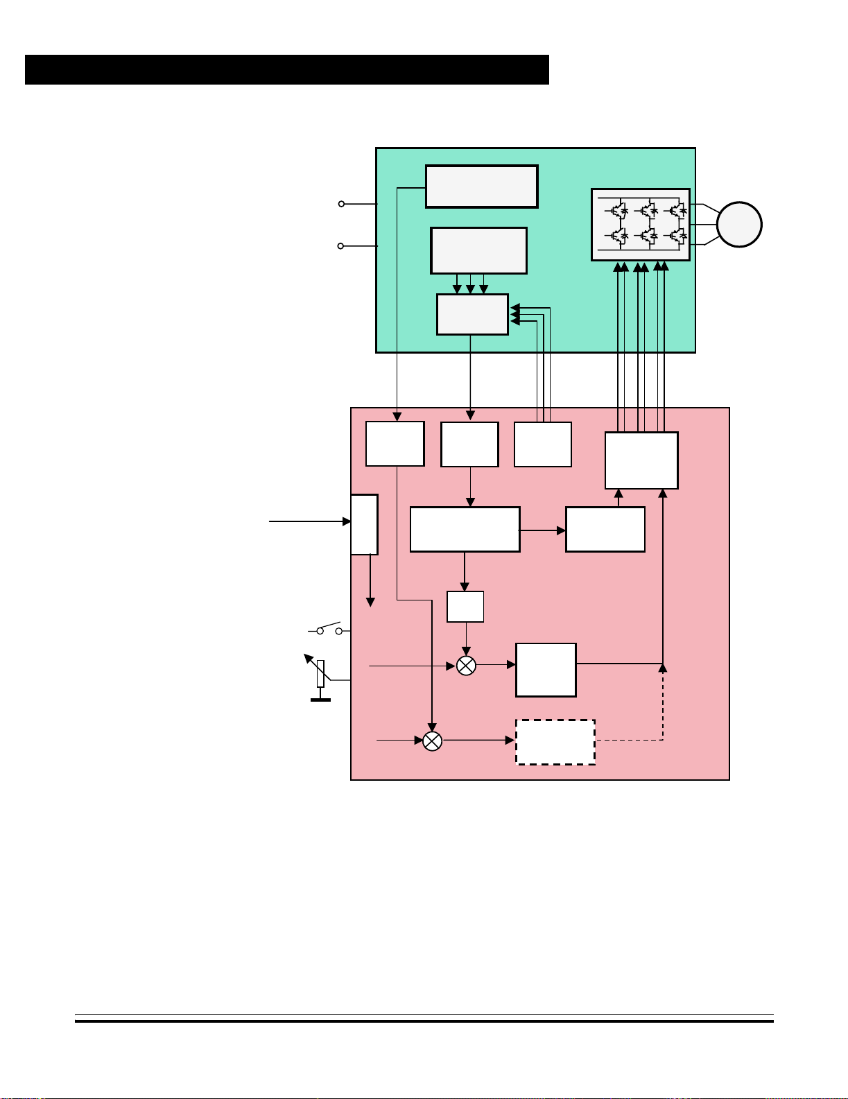
The application block diagram is shown in Figure 2-1. The sensorless
rotor position technique detects the zero crossing points of back-EMF
induced in the motor windings. The phase back-EMF zero crossing
points are sensed while one of the three phase windings is not powered.
The information obtained is processed in order to commutate the
energized phase pair and control the phase voltage, using pulse width
modulation.
The back-EMF zero crossing detection enables position recognition. The
resistor network is used to step down sensed voltages to a 0–3.3 V level.
Zero crossing detection is synchronized with the middle of center aligned
PWM signals by the software, in order to filter high voltage spikes
produced by switching the IGBTs (MOSFETs). The software selects by
MUX command the phase comparator output that corresponds to the
current commutation step. The multiplexer (MUX) circuit selects this
signal, which is then transferred to the MCU input.
The voltage drop resistor is used to measure the dc-bus current which is
chopped by the pulse-width modulator (PWM). The signal obtained is
rectified and amplified (0–3.3 V with 1.65 V offset). The internal MCU
analog-to-digital (A/D) converter and zero crossing detection are
synchronized with the PWM signal. This synchronization avoids spikes
when the IGBTs (or MOSFETs) are switched and simplifies the electric
circuit.
DRM028 — Rev 0 Designer Reference Manual
MOTOROLA System Description 15
For More Information On This Product,
Go to: www.freescale.com
Page 16
System Description
Freescale Semiconductor, Inc.
nc...
I
cale Semiconductor,
Frees
MUX
Command
Commutation
Control
Three-Phase
Inverter
PWM
Generator
Dead Time
with
PWM
Duty
Cycle
HC08MR32
3-ph
BLDC
Motor
DC Bus Current &
DC Bus Voltage
Sensing
Power line
DC-Bus Voltage/
Current
Temperature
ADC
PC Master
START
STOP
SPEED
SCI
Required
Speed
Required
Alignment
Current
3 BEMF Voltage
Zero Crossing
Comparators
MUX
Digital
Inputs
Zero
Crossing
Zero Crossing
Period, Position
Recognition
1/T
Actual
Current
3 phase BLDC
Power Stage
BEMF Zero
Crossing
signal
Digital
Outputs
Zero Crossing
Time moment
Commutation
Period
Actual Speed
Speed PI
Regulator
Current PI
Regulator
(for Alignment)
Figure 2-1System Concept
During the rotor alignment state, the dc-bus current is controlled by the
current PI regulator. In the other states (motor running), the phase
voltage (PWM duty cycle) is controlled by the speed PI regulator.
Designer Reference Manual DRM028 — Rev 0
16 System Description MOTOROLA
For More Information On This Product,
Go to: www.freescale.com
Page 17

Freescale Semiconductor, Inc.
The A/D converter is also used to sense the dc-bus voltage and the drive
temperature. The dc-bus voltage is stepped down to a 3.3-V signal level
by a resistor network.
The six IGBTs (copack with built-in fly back diode), or MOSFETs, and
gate drivers create a compact power stage. The drivers provide the level
shifting that is required to drive the high side switch. The PWM technique
is used to control motor phase voltage.
2.3 System Specification
System Description
System Specification
nc...
I
cale Semiconductor,
Frees
The concept of the application is that of a speed-closed loop drive using
back-EMF zero crossing technique for position detection. It serves as an
example of a sensorless BLDC motor control system using Motorola’s
MC68HC908MR32 MCU. It also illustrates the usage of dedicated motor
control on-chip peripherals.
The system for BLDC motor control consists of hardware and software.
The application uses universal modular motion control development
hardware boards, which are provided by Motorola for customer
development support. For a description of these hardware boards refer
to Appendix A. References 3.,4.,5.,6.,7., and the World Wide Web at:
http://www.motorola.com
There are three board and motor hardware sets for the application:
1. High-Voltage Hardware Set — For variable line voltage 115–230
Vac and medium power (phase current < 2.93 A)
2. Low-Voltage Evaluation Motor Hardware Set — For automotive
voltage (12 V) and very low power (phase current < 4 A)
3. Low-Voltage Hardware Set — For automotive voltage (12 V or
possibly 42 V) and medium power (phase current < 50 A)
DRM028 — Rev 0 Designer Reference Manual
MOTOROLA System Description 17
For More Information On This Product,
Go to: www.freescale.com
Page 18

Freescale Semiconductor, Inc.
System Description
2.3.1 Software Specification
The application software is practically the same for all three hardware
platforms. The only modification needed is to include one of three
constants that customize the hardware and motor parameter settings.
The software (written in C language) specifications are listed in
Table 2-1. A useful feature of the software is serial communication with
PC master software protocol via RS232. The PC master software is PC
computer software which allows reading and setting of all the system
variables, and can also run html script pages to control the application
from the PC. Another feature of the BLDC control software, is on-line
nc...
I
parameter modification with PC master software, which can be used for
software parameter tuning to a customer motor.
cale Semiconductor,
Frees
.
Table 2-1. Software Specifications
3-phase trapezoidal BLDC motor control star or delta!
connected
Control Algorithm
Target Processor MC68HC908MR32
Language C-language with some arithmetical functions in assembler
Compiler Metrowerks ANSI-C/cC++ Compiler for HC08
Application
Control
MCU Oscillator
Frequency
MCU Bus
Frequency
Minimal BLDC
Motor
Commutation
Period
(Without PC
Master
Software
Communication)
Sensorless, with back-EMF zero crossing commutation
control
Speed closed loop control
Motoring mode
Manual interface (start/stop switch, speed potentiometer
control, LED indication)
PC master software (remote) interface (via RS232 using PC
computer)
4 MHz (with default software setting)
8 MHz (with default software setting)
333 µs (with default software setting and COEF_HLFCMT =
0.450)
Designer Reference Manual DRM028 — Rev 0
18 System Description MOTOROLA
For More Information On This Product,
Go to: www.freescale.com
Page 19

nc...
I
cale Semiconductor,
Frees
Freescale Semiconductor, Inc.
Table 2-1. Software Specifications
Minimal BLDC
Motor
Commutation
Period (with PC
Master Software
Control)
Targeted
Hardware
Software
Configuration
and Parameters
Setting
2.3.2 Hardware and Drive Specifications
The other system specifications are determined by hardware boards and
motor characteristics. The boards and their connections are shown in
Section 4. Hardware Design. and Section 6. User Guide, 6.4.1
Hardware Configuration. The hardware set specifications are
discussed in the following subsections.
System Description
System Specification
520 µs (with default software setting and COEF_HLFCMT =
0.450)
Software is prepared to run on three optional board and
motor hardware sets:
• High-voltage hardware set at variable line voltage
115–230 Vac
(software customizing file const_cust_hv.h)
• Low-voltage evaluation motor hardware set
(software customizing file const_cust_evmm.h)
• Low-voltage hardware set (software customizing file
const_cust_lv.h)
Configuration to one of the three required hardware sets is
provided by inclusion of dedicated software customizing
files. The software pack contains the files const_cust_hv.h,
const_cust_lv.h, and const_cust_evm.h with predefined
parameter settings for running on one of the optional board
and motor hardware sets. The required hardware must be
selected in code_fun.c file by one of these files #include.
Where software is configuration for different customer
motors, the software configuration for any motor is
provided in the dedicated customizing file, according to the
hardware board used.
PWM frequency 15.626 kHz with default software setting,
possibly changeable in const.h file
2.3.2.1 High-Voltage Hardware Set Specification
This hardware set is dedicated for medium power (phase current <
2.93 A) and main voltage. The specifications for a high-voltage hardware
DRM028 — Rev 0 Designer Reference Manual
MOTOROLA System Description 19
For More Information On This Product,
Go to: www.freescale.com
Page 20

Freescale Semiconductor, Inc.
System Description
and motor set are listed in Table 2-2. The hardware operates on both
230 Vac and 115 Vac mains.
Table 2-2. High Voltage Hardware Set Specifications
Input voltage: 230 Vac or 115 Vac
Hardware Boards
Characteristics
Motor -Brake Set Manufactured EM Brno, Czech Republic
nc...
I
Maximum dc-bus voltage: 407 V
Maximal output current: 2.93A
EM Brno SM40V
Motor type:
Pole-Number: 6
3 phase, star connected
BLDC motor,
cale Semiconductor,
Frees
Motor Characteristics
Brake Characteristics
Maximum dc-bus voltage: 380 V
Drive Characteristics
Speed range: 2500 rpm (at 310 V)
Maximum electrical
power:
Phase voltage: 3*220 V
Phase current: 0.55 A
Brake Type:
Nominal Voltage: 3 x 27 V
Nominal Current: 2.6 A
Pole-Number: 6
Nominal Speed: 1500 rpm
Speed range:
Optoisolation: Required
Protection:
150 W
SG40N
3-Phase BLDC Motor
< 2500 rpm
(determined by motor
used)
Over-current,
over-voltage, and
under-voltage fault
protection
Load Characteristic Type: Varying
Designer Reference Manual DRM028 — Rev 0
20 System Description MOTOROLA
For More Information On This Product,
Go to: www.freescale.com
Page 21

Freescale Semiconductor, Inc.
System Description
System Specification
2.3.2.2 Low-Voltage Evaluation Hardware Set Specification
This hardware set is dedicated for 12 V voltage and very low power
(phase current < 4 A). The specifications for a low-voltage evaluation
hardware and motor set are listed in Table 2-3. It is targeted first of all to
software evaluation with small motors.
Table 2-3. Low Voltage Evaluation Hardware Set Specifications
Input voltage: 12 Vdc
nc...
I
Hardware Boards
Characteristics
Maximum dc-bus voltage: 16.0 V
Maximal output current: 4.0 A
cale Semiconductor,
Frees
Motor Characteristics
Drive Characteristics
Load Characteristic Type: Varying
2.3.2.3 Low-Voltage Hardware Set Specification
Motor type:
Speed range: < 5000 rpm (at 60 V)
Maximal line voltage: 60 V
Phase current: 2 A
Output torque: 0.140 Nm (at 2 A)
Speed range: < 1400 rpm
Input voltage: 12 Vdc
Maximum dc-bus voltage: 15.8 V
Protection:
4 poles, three phase, star
connected, BLDC motor
Over-current,
over-voltage, and
under-voltage fault
protection
This hardware set is dedicated for medium power (phase current < 50 A)
and automotive voltage. The specifications for a low-voltage hardware
and motor set are listed in Table 2-4. The hardware power stage board
is dedicated for 12 V, but can be simply configured to a 42 V supply
(described in documentation for the ECLOVACBLDC board). The
supplied motor is targeted for 12 V.
DRM028 — Rev 0 Designer Reference Manual
MOTOROLA System Description 21
For More Information On This Product,
Go to: www.freescale.com
Page 22

System Description
Freescale Semiconductor, Inc.
Table 2-4. Low Voltage Hardware Set Specifications
Input voltage: 12 Vdc or 42 V
Hardware Boards
Characteristics
Motor -Brake Set Manufactured EM Brno, Czech Republic
Maximum dc-bus voltage: 16.0 V or 55.0 V
Maximal output current: 50.0 A
EM Brno SM40N
Motor type:
Pole-Number: 6
3 phase, star connected
BLDC motor,
nc...
I
cale Semiconductor,
Frees
Motor Characteristics
Brake Characteristics
Drive Characteristics
Maximum dc-bus voltage: 15.8 V
Speed range: 3000 rpm (at 12 V)
Maximum electrical
power:
Phase voltage: 3*6.5 V
Phase current: 17 A
Brake Type:
Nominal Voltage: 3 x 27 V
Nominal Current: 2.6 A
Pole-Number: 6
Nominal Speed: 1500 rpm
Speed range: < 2500 rpm
Input voltage: 12 Vdc
Protection:
150 W
SG40N
3-Phase BLDC Motor
Over-current,
over-voltage, and
under-voltage fault
protection
Load Characteristic Type: Varying
Designer Reference Manual DRM028 — Rev 0
22 System Description MOTOROLA
For More Information On This Product,
Go to: www.freescale.com
Page 23

Freescale Semiconductor, Inc.
Designer Reference Manual — Sensorless BLDC Motor Control
Section 3. BLDC Motor Control
3.1 Contents
3.2 Brushless DC Motor Control Theory. . . . . . . . . . . . . . . . . . . . .23
3.3 Used Control Technique . . . . . . . . . . . . . . . . . . . . . . . . . . . . . . 38
nc...
I
cale Semiconductor,
Frees
3.4 Application Control . . . . . . . . . . . . . . . . . . . . . . . . . . . . . . . . . .50
3.2 Brushless DC Motor Control Theory
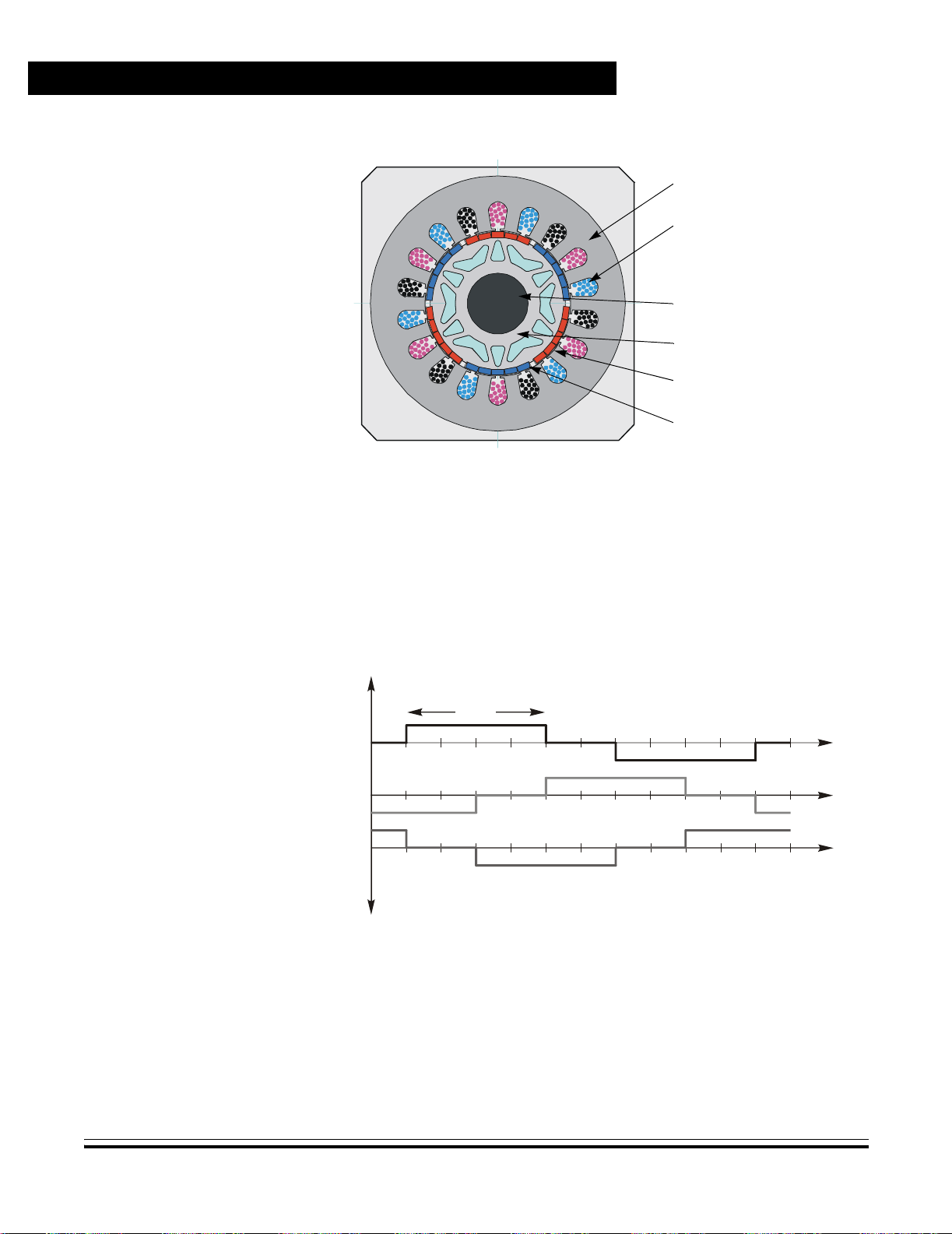
3.2.1 BLDC Motor Targeted by This Application
The brushless dc motor (BLDC motor) is also referred to as an
electronically commutated motor. There are no brushes on the rotor, and
commutation is performed electronically at certain rotor positions. The
stator magnetic circuit is usually made from magnetic steel sheets.
Stator phase windings are inserted in the slots (distributed winding) as
shown in Figure 3-1, or it can be wound as one coil on the magnetic
pole. Magnetization of the permanent magnets and their displacement
on the rotor are chosen in such a way that the back-EMF (the voltage
induced into the stator winding due to rotor movement) shape is
trapezoidal. This allows a rectangular shaped 3-phase voltage system
(see Figure 3-2) to be used to create a rotational field with low torque
ripples.
DRM028 — Rev 0 Designer Reference Manual
MOTOROLA BLDC Motor Control 23
For More Information On This Product,
Go to: www.freescale.com
Page 24
BLDC Motor Control
Freescale Semiconductor, Inc.
STATOR
STATOR WINDING
(IN SLOTS)
SHAFT
ROTOR
AIR GAP
nc...
I
cale Semiconductor,
Frees
PERMANENT MAGNETS
Figure 3-1. BLDC Motor Cross Section
The motor can have more than just one pole-pair per phase. This defines
the ratio between the electrical revolution and the mechanical revolution.
The BLDC motor shown has three pole-pairs per phase, which represent
three electrical revolutions per one mechanical revolution.
Voltage
VOLTAGE
Phase A
PHASE A
Phase B
PHASE B
Phase C
PHASE C
30° 90° 150° 210° 270° 330°
30° 90° 150° 210° 270° 330°
120°
120°
ELECTRICAL
electrical
ANGLE
angle
Figure 3-2. 3-Phase Voltage System
The easy to create rectangular shape of applied voltage ensures the
simplicity of control and drive. But, the rotor position must be known at
certain angles in order to align the applied voltage with the back-EMF
(voltage induced due to movement of the PM). The alignment between
Designer Reference Manual DRM028 — Rev 0
24 BLDC Motor Control MOTOROLA
For More Information On This Product,
Go to: www.freescale.com
Page 25

Freescale Semiconductor, Inc.
back-EMF and commutation events is very important. In this condition,
the motor behaves as a dc motor and runs at the best working point.
Thus, simplicity of control and good performance make this motor a
natural choice for low-cost and high-efficiency applications.
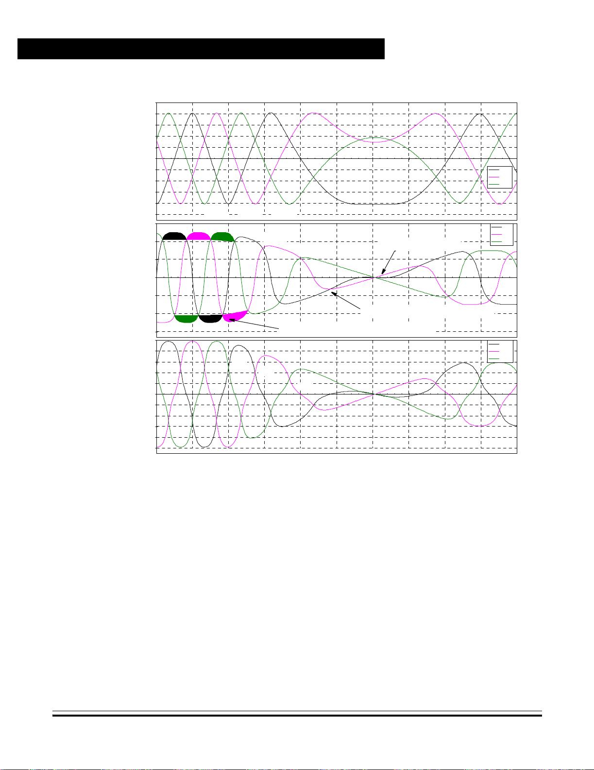
Figure 3-3 shows a number of waveforms:
• Magnetic flux linkage
• Phase back-EMF voltage
• Phase-to-phase back-EMF voltage
Magnetic flux linkage can be measured. However, in this case it was
nc...
I
calculated by integrating the phase back-EMF voltage (which was
measured on the non-fed motor terminals of the BLDC motor). As can
be seen, the shape of the back-EMF is approximately trapezoidal and
the amplitude is a function of the actual speed. During speed reversal,
the amplitude changes its sign and the phase sequence changes.
BLDC Motor Control
Brushless DC Motor Control Theory
cale Semiconductor,
Frees
DRM028 — Rev 0 Designer Reference Manual
MOTOROLA BLDC Motor Control 25
For More Information On This Product,
Go to: www.freescale.com
Page 26
BLDC Motor Control
Phase Magnetic
Flux Linkage
Freescale Semiconductor, Inc.
Ps i_ A
Ps i_ B
Ps i_ C
nc...
I
cale Semiconductor,
Frees
PH. A
Phase Back EMF
Atop Btop Ctop
Cbot Abot Bbot
Phase-Phase
Back EMF
Figure 3-3. BLDC Motor Back EMF and Magnetic Flux
The filled areas in the tops of the phase back-EMF voltage waveforms
PH. A
A–B
PH. B
PH. C
PH. B
PH. C
“NATURAL” COMMUTATION POINT
“Natural” commutation point
ACTING POWER SWITCH IN THE POWER STAGE
B–C
C–A
SPEED REVERSAL
Speed reversal
Ui_A
Ui_B
Ui_C
Ui_A B
Ui_B C
Ui_CA
indicate the intervals where the particular phase power stage
commutations occur. The power switches are cyclically commutated
through the six steps; therefore, this technique is sometimes called six
step commutation control. The crossing points of the phase back-EMF
voltages represent the natural commutation points. In normal operation
the commutation is performed here. Some control techniques advance
the commutation by a defined angle in order to control the drive above
the pulse-width modulator (PWM) voltage control.
Designer Reference Manual DRM028 — Rev 0
26 BLDC Motor Control MOTOROLA
For More Information On This Product,
Go to: www.freescale.com
Page 27
Freescale Semiconductor, Inc.
BLDC Motor Control
Brushless DC Motor Control Theory
3.2.2 3-Phase BLDC Power Stage
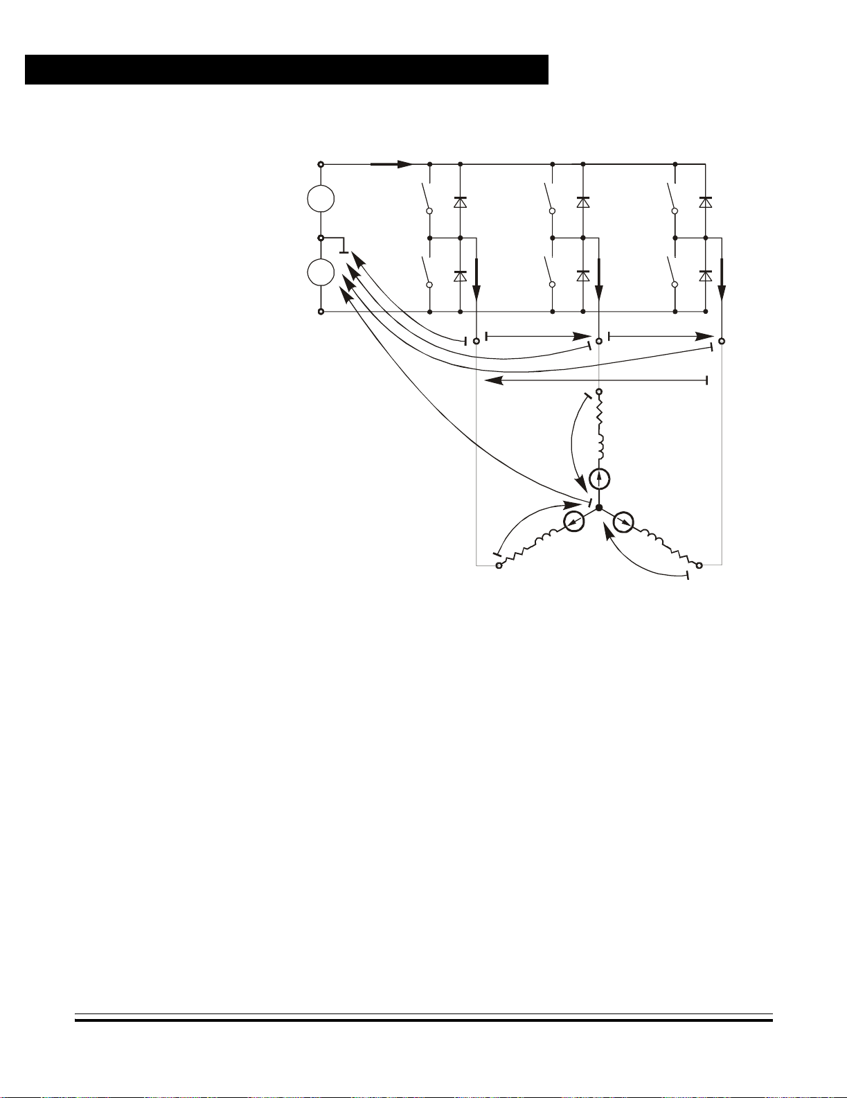
The voltage for 3-phase BLDC motor is provided by a 3-phase power
stage controlled by digital signals. Its topology is the one as for the AC
induction motor (refer to Figure 3-5). The power stage is usually
controlled by a dedicated microcontroller with on-chip PWM module.
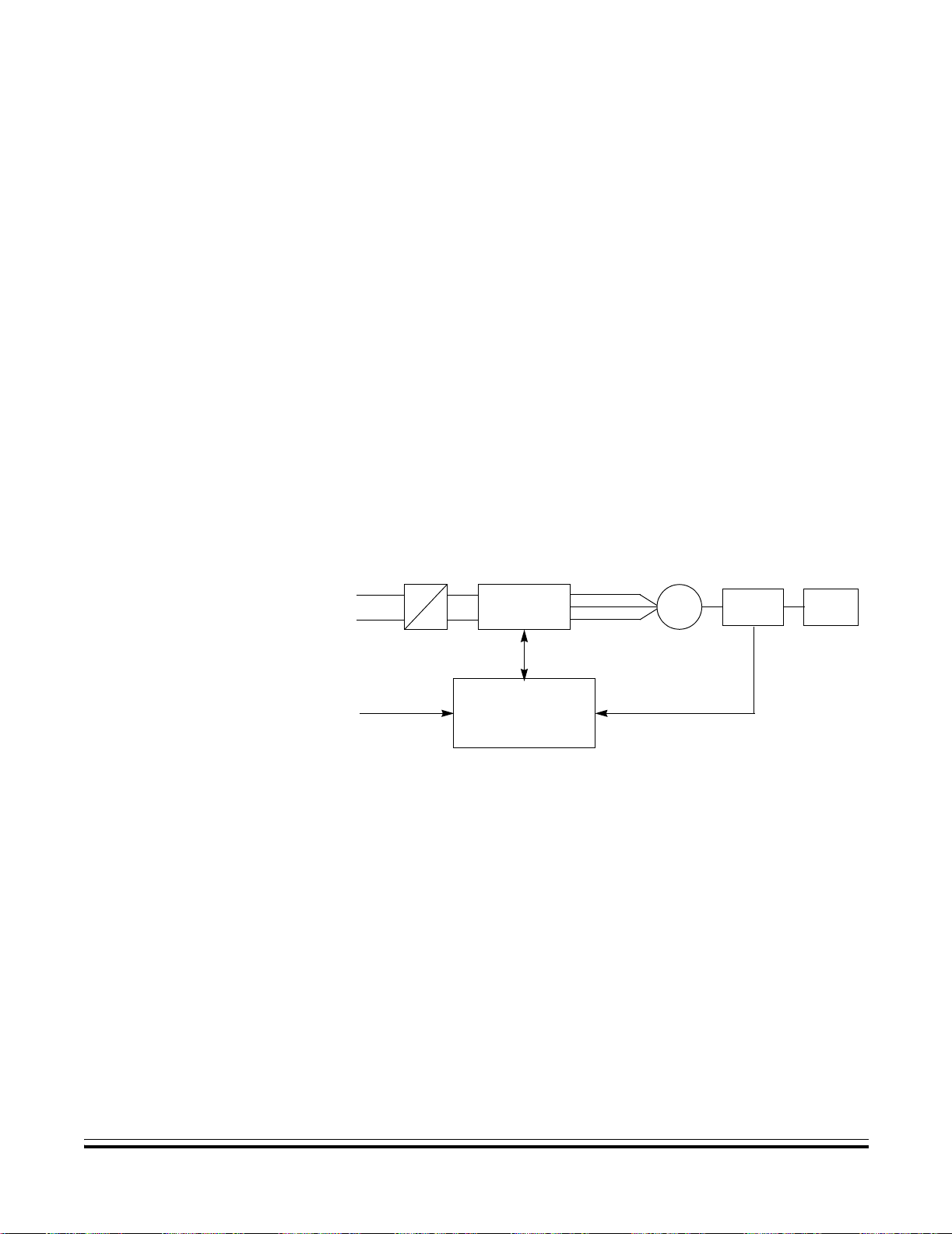
3.2.3 Why Sensorless Control?
As explained in the previous section, rotor position must be known in
order to drive a brushless dc motor. If any sensors are used to detect
rotor position, sensed information must be transferred to a control unit
nc...
I
(see Figure 3-4). Therefore, additional connections to the motor are
necessary. This may not be acceptable for some applications (see 1.3
Benefits of the Solution).
cale Semiconductor,
Frees
AC LINE VOLTAGE
SPEED
SETTING
–
=
CONTROL SIGNALS
3.2.4 Power Stage — Motor System Model
In order to explain and simulate the idea of back-EMF sensing
techniques a simplified mathematical model based on the basic circuit
topology has been created. See Figure 3-5.
POWER STAGE
CONTROL UNIT
MOTOR DRIVE
M
POSITION FEEDBACK
Figure 3-4. Classical System
POSITION
SENSORS
LOAD
DRM028 — Rev 0 Designer Reference Manual
MOTOROLA BLDC Motor Control 27
For More Information On This Product,
Go to: www.freescale.com
Page 28
BLDC Motor Control
Freescale Semiconductor, Inc.
u
d
/2
u
d
/2
I
d0
+
S
=
-
+
=
-
At
S
Ab
S
Bt
I
S
Sa
Bb
S
Ct
I
S
Sb
Cb
I
Sc
u
VA
nc...
I
u
AB
u
VB
u
Sb
u
0
u
Sa
u
backEMF a
u
La
uu
Ra Rc
O
A
Figure 3-5. Power Stage — Motor Topology
The second goal of the model is to find how the motor characteristics
cale Semiconductor,
depend on the switching angle. The switching angle is the angular
difference between a real switching event and an ideal one (at the point
where the phase-to-phase back-EMF crosses zero).
u
VC
u
CA
B
u
Rb
u
Lb
u
backEMF b
u
u
Sc
u
BC
backEMF c
u
Lc
C
Frees
The motor-drive model consists of a normal 3-phase power stage plus a
brushless dc motor. Power for the system is provided by a voltage
source (U
). Six semiconductor switches (S
d
A/B/C t/b
), controlled
elsewhere, allow the rectangular voltage waveforms (see Figure 3-2) to
be applied.
The semiconductor switches and diodes are simulated as
ideal devices. The natural voltage level of the whole model is put at one
half of the dc-bus voltage. This simplifies the mathematical expressions.
Designer Reference Manual DRM028 — Rev 0
28 BLDC Motor Control MOTOROLA
For More Information On This Product,
Go to: www.freescale.com
Page 29

Freescale Semiconductor, Inc.
3.2.4.1 Stator Winding Equations
The BLDC motor is usually very symmetrical. All phase resistances,
phase and mutual inductances, flux-linkages can be thought of as equal
to, or as a function of the position θ with a 120° displacement.
The electrical BLDC motor model then consists of a set of the following
stator voltage equations (EQ 3-1.).
BLDC Motor Control
Brushless DC Motor Control Theory
nc...
I
cale Semiconductor,
Frees
The task of this section is to explain the background of the back-EMF
sensing and to demonstrate how the zero crossing events can be
detected. Parasitic effects that negatively influence the back-EMF
detection are discussed and their nature analyzed.
3.2.4.2 Indirect Back EMF Sensing
Let us assume a usual situation, where the BLDC motor is driven in
six-step commutation mode using PWM technique, where both top and
bottom switches in the diagonal are controlled using the same signal (so
called “hard switching PWM” technique). The motor phases A and B are
powered, and phase C is free, having no current. So the phase C can be
used to sense the back-EMF voltage. This is described by the following
conditions:
VB
Sc
Ψ
Sa
d
+=
Ψ
Sb
td
Ψ
Sc
1
=,
---± u
2
d–id==,
Sb
u
Sa
u
Sb
u
Sc
SAbSBt, PWM←
u
VA
i
iSb–i==i
Sa
u
backEMF aubackEMF bubackEMF c
++ 0=
i
Sa
R
i
S
Sb
i
Sc
1
−
=u
---u
+
d
2
di
Sa
0=i
Sc
d0=,
i
(EQ 3-1.)
d
(EQ 3-2.)
The branch voltage u
u
DRM028 — Rev 0 Designer Reference Manual
MOTOROLA BLDC Motor Control 29
For More Information On This Product,
Go to: www.freescale.com
VC
u
Vc
1
---u
Sc
3
xa=
can be calculated using the above conditions,
c
∑
backEMF x
LacLbc–()
id
---- uVC–+–=
td
(EQ 3-3.)
Page 30

BLDC Motor Control
After evaluation the expression of the branch voltage uVc is as follows:
Freescale Semiconductor, Inc.
nc...
I
cale Semiconductor,
Frees
VC
3
---u
backEMF c
2
u
1
–()
---L
acLbc
2
id
(EQ 3-4.)
----–=
td
The same expressions can also be found for phase A and B:
3
VA
VB
---u
backEMF a
2
3
---u
backEMF b
2
u
u
1
–()
---L
baLca
2
1
–()
---L
cbLab
2
id
----–=
td
id
----–=
td
(EQ 3-5.)
(EQ 3-6.)
The first member in the equation (EQ 3-6.) demonstrates the possibility
to indirectly sense the back-EMF between the free (not powered) phase
terminal and the zero point, defined at half of the dc-bus voltage (see
Figure 3-5.). Simple comparison of these two levels can provide the
required zero crossing detection.
As shown in Figure 3-5, the branch voltage of phase B can be sensed
between the power stage output B and the zero voltage level. Thus,
back-EMF voltage is obtained and the zero crossing can be recognized.
When Lcb = Lab, this general expressions can also be found:
3
u
---u
Vx
backEMFx
2
where x A B C,,==
(EQ 3-7.)
There are two necessary conditions which must be met:
• Top and bottom switches (in diagonal) have to be driven with the
same PWM signal
• No current goes through the non-fed phase that is used to sense
the back-EMF
Figure 3-6 shows branch and motor phase winding voltages during a
0–360° electrical interval. Shaded rectangles designate the validity of
the equation (EQ 3-7.). In other words, the back-EMF voltage can be
sensed during designated intervals.
Designer Reference Manual DRM028 — Rev 0
30 BLDC Motor Control MOTOROLA
For More Information On This Product,
Go to: www.freescale.com
Page 31

Freescale Semiconductor, Inc.
0 30 60 90 120 150 180 210 240 270 300 330 360 390
BLDC Motor Control
Brushless DC Motor Control Theory
uVA
uSa
- Back-EMF can be sensed
Figure 3-6. Phase Voltage Waveform
nc...
I
However simple this solution looks, in reality it is more difficult, because
the sensed “branch” voltage also contains some ripples.
cale Semiconductor,
Frees
3.2.4.3 Effect of Mutual Inductance
As shown in previous equations (EQ 3-4.) through (EQ 3-6.), the mutual
inductances play an important role here. The difference of the mutual
inductances between the coils which carry the phase current, and the
coil used for back-EMF sensing, causes the PWM pulses to be
superimposed onto the detected back-EMF voltage. In fact, it is
produced by the high rate of change of phase current, transferred to the
free phase through the coupling of the mutual inductance.
Figure 3-7 shows the real measured “branch” voltage. The red curves
highlight the effect of the difference in the mutual inductances. This
difference is not constant.
DRM028 — Rev 0 Designer Reference Manual
MOTOROLA BLDC Motor Control 31
For More Information On This Product,
Go to: www.freescale.com
Page 32

BLDC Motor Control
Freescale Semiconductor, Inc.
0 V
Figure 3-7. Mutual Inductance Effect
nc...
I
cale Semiconductor,
Frees
Due to the construction of the BLDC motor, both mutual inductances
vary. They are equal at the position that corresponds to the back-EMF
zero crossing detection.
The branch waveform detail is shown in Figure 3-8. Channel 1 in
Figure 3-8 shows the disturbed “branch” voltage. The superimposed
ripples clearly match the width of the PWM pulses, and thus prove the
conclusions from the theoretical analysis.
The effect of the mutual inductance corresponds well in observations
carried out on the five different BLDC motors. These observations were
made during the development of the sensorless technique.
NOTE: The BLDC motor with stator windings distributed in the slots has
technically higher mutual inductances than other types. Therefore, this
effect is more significant. On the other hand the BLDC motor with
windings wounded on separate poles, shows minor presence of the
effect of mutual inductance.
CAUTION: However noticeable this effect, it does not degrade the back-EMF zero
crossing detection because it is cancelled at the zero crossing point.
Simple additional filtering helps to reduce ripples further.
Designer Reference Manual DRM028 — Rev 0
32 BLDC Motor Control MOTOROLA
For More Information On This Product,
Go to: www.freescale.com
Page 33

Freescale Semiconductor, Inc.
nc...
I
BLDC Motor Control
Brushless DC Motor Control Theory
cale Semiconductor,
Frees
Figure 3-8. Detail of Mutual Inductance Effect
3.2.4.4 Effect of Mutual Phase Capacitance
The negative effect of mutual inductance is not the only one to disturb
the back-EMF sensing. So far, the mutual capacitance of the motor
phase windings was neglected in the motor model, since it affects
neither the phase currents nor the generated torque. Usually the mutual
capacitance is very small. Its influence is only significant during PWM
switching, when the system experiences very high du/dt.
The effect of the mutual capacitance can be studied using the model
shown in Figure 3-9.
DRM028 — Rev 0 Designer Reference Manual
MOTOROLA BLDC Motor Control 33
For More Information On This Product,
Go to: www.freescale.com
Page 34

Freescale Semiconductor, Inc.
BLDC Motor Control
I
d0
+
u
d
/2
u
d
/2
S
=
-
+
=
-
At
S
Ab
S
Bt
u
VA
S
Bb
I
Sb
Figure 3-9. Mutual Capacitance Model
nc...
I
Let us focus on the situation when the motor phase A is switched from
negative dc-bus rail to positive, and the phase B is switched from
positive to negative. This is described by these conditions (EQ 3-8.):
A
i
C
R
C
i
Cab
u
Cba
C
B
u
VB
u
Cac
C
R
C
C
i
C
C
R
u
C
Ccb
u
VC Cap
cale Semiconductor,
Frees
SAbSBt, PWM←
1
1
–
u
VA
---u
→=u
---u
d
2
d
2
==
i
CaciCcbiC
The voltage that disturbs the back-EMF sensing, utilizing the free (not
powered) motor phase C, can be calculated based the equation:
u
VC Cap
1
++()u
---u
CcbuCac
2
2R
C
The final expression for disturbing voltage can be found as follows:
u
VC Cap
1
==
---
2
1
-------C
1
--------–
iCtd
∫
C
ac
cb
1
---u
VB
d
2
+()–
CcbRC
C
1
cbCac
---
----------------------
2
C
cbCac
1
–→=,
---u
d
2
1
---u
–()==
CacuCcb
2
–
⋅
td
i
C
∫
(EQ 3-8.)
(EQ 3-9.)
(EQ 3-10.)
NOTE: (EQ 3-10.) expresses the fact that only the unbalance of the mutual
capacitance (not the capacitance itself) disturbs the back-EMF sensing.
When both capacities are equal (they are balanced), the disturbances
disappear. This is demonstrated in Figure 3-10 and Figure 3-11.
Designer Reference Manual DRM028 — Rev 0
34 BLDC Motor Control MOTOROLA
For More Information On This Product,
Go to: www.freescale.com
Page 35

Freescale Semiconductor, Inc.
nc...
I
BLDC Motor Control
Brushless DC Motor Control Theory
cale Semiconductor,
Frees
Figure 3-10. Distributed Back-EMF by Unbalanced
Capacity Coupling
Channel 1 in Figure 3-11 shows the disturbed “branch” voltage, while
the other phase (channel 2) is not affected because it faces balanced
mutual capacitance. The unbalance was purposely made by adding a
small capacitor on the motor terminals, in order to better demonstrate
the effect. After the unbalance was removed the “branch” voltage is
clean, without any spikes.
DRM028 — Rev 0 Designer Reference Manual
MOTOROLA BLDC Motor Control 35
For More Information On This Product,
Go to: www.freescale.com
Page 36

Freescale Semiconductor, Inc.
BLDC Motor Control
nc...
I
cale Semiconductor,
Frees
NOTE: The configuration of the phase windings end-turns has significant
impact; therefore, it needs to be properly managed to preserve the
balance in the mutual capacity. This is important, especially for prototype
motors that are usually hand-wound.
CAUTION: Failing to maintain balance in the mutual capacitance can easily
disqualify such a motor from using sensorless techniques based on the
back-EMF sensing. Usually, the BLDC motors with windings wound on
separate poles show minor presence of the mutual capacitance. Thus,
the disturbance is also insignificant.
3.2.5 Back-EMF Sensing Circuit
An example of the possible implementation of the back-EMF sensing
circuit is shown in Figure 3-12.
Figure 3-11. Balanced Capacity Coupling
Designer Reference Manual DRM028 — Rev 0
36 BLDC Motor Control MOTOROLA
For More Information On This Product,
Go to: www.freescale.com
Page 37

Freescale Semiconductor, Inc.
+DC_BUS PHASE A PHASE B PHASE C
BLDC Motor Control
Brushless DC Motor Control Theory
nc...
I
cale Semiconductor,
Frees
560k
560k
560k
2x27k
560k
560k
560k
2x27k 2x27k 2x27k
1n
560k
560k
560k
1n
+
–
1n
1n
+
–
+
–
MUX
ZERO
CROSSING
DETECTION
SIGNAL
MUX COMMAND
Figure 3-12. Back-EMF Sensing Circuit Diagram
As explained in the theoretical part of this designer reference manual,
the phase zero crossing event can be detected at the moment when the
branch voltage (of a free phase) crosses the half dc-bus voltage level.
The resistor network is used to step down sensed voltages down to a
0–15 V voltage level. The comparators sense the zero voltage difference
in the input signal. The multiple resistors reduce the voltage across each
resistor component to an acceptable level. A simple RC filter prevents
the comparators from being disturbed by high voltage spikes produced
by IGBT switching. The multiplexer (MUX) selects the phase comparator
output, which corresponds to the current commutation stage. This zero
crossing detection signal is transferred to the timer input pin.
The comparator control and zero crossing signals plus the voltage
waveforms are shown in Figure 3-13.
DRM028 — Rev 0 Designer Reference Manual
MOTOROLA BLDC Motor Control 37
For More Information On This Product,
Go to: www.freescale.com
Page 38

Freescale Semiconductor, Inc.
BLDC Motor Control
Phase Selection
MUX Command
Phase Comparator
Output
(Zero crossing edge)
"Branch" Voltage
(Interval of phase
Back-EMF zero
crossing detection)
Reference Level
nc...
I
Commutation
Signal
Zero Crossing
Signal
90°
cale Semiconductor,
Frees
3.3 Used Control Technique
3.3.1 Sensorless Commutation Control
This section concentrates on sensorless BLDC motor commutation with
back-EMF zero crossing technique.
In order to start and run the BLDC motor, the control algorithm has to go
through the following states:
• Alignment
• Starting (Back-EMF Acquisition)
• Running
Figure 3-14 shows the transitions between the states. First the rotor is
aligned to a known position; then the rotation is started without the
position feedback. When the rotor moves, back-EMF is acquired so the
Figure 3-13. The Zero Crossing Detection
Designer Reference Manual DRM028 — Rev 0
38 BLDC Motor Control MOTOROLA
For More Information On This Product,
Go to: www.freescale.com
Page 39

Freescale Semiconductor, Inc.
BLDC Motor Control
Used Control Technique
position is known, and can be used to calculate the speed and
processing of the commutation in the running state.
START MOTOR
ALIGNMENT
nc...
I
cale Semiconductor,
Frees
3.3.1.1 Alignment
ALIGNMENT TIME
EXPIRED?
YES
STARTING
(BACK-EMF ACQUISITION)
MINIMAL CORRECT
COMMUTATIONS DONE?
YES
RUNNING
NO
NO
Figure 3-14. Commutation Control Stages
Before the motor starts, there is a short time (depending on the motor’s
electrical time constant) when the rotor position is stabilized by applying
PWM signals to only two motor phases (no commutation). The current
controller keeps current within predefined limits. This state is necessary
in order to create a high start-up torque. When the preset time-out
expires then this state is finished.
DRM028 — Rev 0 Designer Reference Manual
MOTOROLA BLDC Motor Control 39
For More Information On This Product,
Go to: www.freescale.com
Page 40

Freescale Semiconductor, Inc.
BLDC Motor Control
The current controller subroutine, with PI regulator, is called to control
dc-bus current. It sets the correct PWM ratio for the required current. The
current PI controller works with constant execution (sampling) period.
This period should be a multiple of the PWM period, in order to
synchronize the current measurement with PWM:
Current controller period = n/PWM frequency
The BLDC motor rotor position with flux vectors during alignment is
shown in Figure 3-15.
nc...
I
cale Semiconductor,
Frees
3.3.1.2 Running
Figure 3-15. Alignment
The commutation process is a series of states which assure:
• The back-EMF zero crossing is successfully captured
• The new commutation time is calculated
• The commutation is performed
The following processes need to be provided:
Designer Reference Manual DRM028 — Rev 0
40 BLDC Motor Control MOTOROLA
For More Information On This Product,
Go to: www.freescale.com
Page 41

Freescale Semiconductor, Inc.
• BLDC motor commutation service
• Back-EMF zero crossing moment capture service
• Calculation of commutation time
• Interactions between these commutation processes
From diagrams an overview of how the commutation works can be
understood. After commuting the motor phases, there is a time interval
(Per_Toff[n]) when the shape of back-EMF must stabilized (after the
commutation the fly-back diodes are conducting the decaying phase
current; therefore, sensing of the back-EMF is not possible). Then the
new commutation time (T2[n]) is preset. The new commutation will be
nc...
I
performed at this time if the back-EMF zero crossing is not captured. If
the back-EMF zero crossing is captured before the preset commutation
time expires, then the exact calculation of the commutation time (T2*[n])
is made, based on the captured zero crossing time (T_ZCros[n]). The
new commutation is performed at this new time.
BLDC Motor Control
Used Control Technique
cale Semiconductor,
Frees
If for any reason the back-EMF feedback is lost within one commutation
period, corrective actions are taken in order to return to the regular
states.
The flowchart explaining the principle of BLDC commutation control with
back-EMF zero crossing sensing is shown in Figure 3-16.
DRM028 — Rev 0 Designer Reference Manual
MOTOROLA BLDC Motor Control 41
For More Information On This Product,
Go to: www.freescale.com
Page 42

BLDC Motor Control
Freescale Semiconductor, Inc.
COMMUTATION DONE
nc...
I
cale Semiconductor,
Frees
BEMF ZERO CROSSING
DETECTED BETWEEN PREVIOUS
COMMUTATIONS?
YES
SERVICE OF COMMUTATION:
PRESET COMMUTATION
WAIT FOR PER_TOFF UNTIL PHASE
CURRENT DECAYS TO ZERO
BEMF ZERO CROSSING
MISSED?
BEMF ZERO CROSSING
NO
HAS COMMUTATION
NO
DETECTED?
NO
TIME EXPIRED?
YES
NO
YES
YES
MAKE MOTOR COMMUTATION
CORRECTIVE CALCULATION 1.
SERVICE OF RECEIVED BEMF
ZERO CROSSING:
CORRECTED SETTING
OF COMMUTATION TIME
HAS COMMUTATION
BEMF ZERO CROSSING MISSED
CORRECTIVE CALCULATION 2
CORRECTED SETTING
OF COMMUTATION TIME
TIME EXPIRED?
YES
NO
Figure 3-16. BLDC Commutation with Back-EMF
Zero Crossing Sensing Flowchart
3.3.1.3 Running — Commutation Time Calculation
Commutation time calculation is shown in Figure 3-17.
Designer Reference Manual DRM028 — Rev 0
42 BLDC Motor Control MOTOROLA
For More Information On This Product,
Go to: www.freescale.com
Page 43

Freescale Semiconductor, Inc.
BLDC Motor Control
Used Control Technique
nc...
I
cale Semiconductor,
Frees
T_Cmt[n-2]
T2[n-3] T2[n-2] T2[n-1] T2[n]
T_Cmt[n-1] T_Cmt[n]
n-2
ZERO CROSSING
DETECTION SIGNAL
Per_ZCros0[n] =
Per_ZCros[n-1]Per_ZCros[n-2]
n-1
ZERO CROSSING
DETECTION SIGNAL
T_ZCros[n-1]
Per_Toff[n]
ZERO CROSSING
DETECTION SIGNAL
2*Per_ZCrosFlt[n-1]
Per_ZCros[n]
Per_ZCros[n]
n
Per_ZCros[n]
Per_HlfCmt[n]
T_ZCros[n]
T_Cmt**[n+1]
Per_HlfCmt[n]
Figure 3-17. BLDC Commutation Time with Zero Crossing Sensing
The following calculations are made to calculate the commutation time
(T2[n]) during the Running state:
• Service of commutation — The commutation time (T2[n]) is
predicted:
T2[n] = T_Cmt[n] + 2*Per_ZCrosFlt[n-1]
If 2*Per_ZCrosFlt>Per_Cmt_Max
then result is limited at Per_Cmt_Max
COMMUTATION IS PRESET
COMMUTATED AT PRESET TIME NO
BACK-BMF FEEDBACK WAS RECEIVED
CORRECTIVE CALCULATION 1.
T_Cmt*[n+1]
BACK-EMF FEEDBACK
RECEIVED AND EVALUATED
COMMUTATED WHEN BACK-EMF
ZERO CROSSING IS MISSED
CORRECTION CALCULATION 2.
• Service of received back-EMF zero crossing — The
commutation time (T2*[n]) is evaluated from the captured
back-EMF zero crossing time (T_ZCros[n]):
Per_ZCros[n] = T_ZCros[n] - T_ZCros[n-1] = T_ZCros[n] - T_ZCros0
Per_ZCrosFlt[n] = (1/2*Per_ZCros[n]+1/2*Per_ZCros0)
HlfCmt[n] = 1/2*Per_ZCrosFlt[n]- Advance_angle =
= 1/2*Per_ZCrosFlt[n]- C_CMT_ADVANCE*Per_ZCrosFlt[n]=
Coef_HlfCmt*Per_ZCrosFlt[n]
DRM028 — Rev 0 Designer Reference Manual
MOTOROLA BLDC Motor Control 43
For More Information On This Product,
Go to: www.freescale.com
Page 44

nc...
I
cale Semiconductor,
Frees
BLDC Motor Control
Freescale Semiconductor, Inc.
Per_Toff[n+1] = Per_ZCrosFlt*Coef_Toff and Per_Dis minimum
Per_ZCros0 <-- Per_ZCros[n]
T_ZCros0 <-- T_ZCros[n]
T2*[n] = T_ZCros[n] + HlfCmt[n]
The best commutation was get with Advance_angle:
60Deg*1/8 = 7.5Deg
which means Coef_HlfCmt = 0.375 at Running state
with default s/w setting
Coef_Toff = 0.375 at Running state, Per_Dis = 150
with default s/w setting
• If no back-EMF zero crossing was captured during preset
commutation period (T2P[n] then Corrective Calculation 1. is
made:
T_ZCros[n] <-- CmtT[n+1]
Per_ZCros[n] = T_ZCros[n] - T_ZCros[n-1] = T_ZCros[n] - T_ZCros0
Per_ZCrosFlt[n] = (1/2*Per_ZCros[n]+1/2*Per_ZCros0)
HlfCmt[n] = 1/2*Per_ZCrosFlt[n]-Advance_angle =
Coef_HlfCmt*Per_ZCrosFlt[n]
The best commutation was get with Advance_angle:
60Deg*1/8 = 7.5Deg
which means Coef_HlfCmt = 0.375 at Running state!
Per_Toff[n+1] = Per_ZCrosFlt*Coef_Toff and Per_Dis minimum
Per_ZCros0 <-- Per_ZCros[n]
T_ZCros0 <-- T_ZCros[n]
• If back-EMF zero crossing is missed then Corrective Calculation
2. is made:
T_ZCros[n] <-- CmtT[n]+Toff[n]
Per_ZCros[n] = T_ZCros[n] - T_ZCros[n-1] = T_ZCros[n] - T_ZCros0
Per_ZCrosFlt[n] = (1/2*T_ZCros[n]+1/2*T_ZCros0)
HlfCmt[n] = 1/2*Per_ZCrosFlt[n]-Advance_angle =
Coef_HlfCmt*Per_ZCrosFlt[n]
The best commutation was get with Advance_angle:
60Deg*1/8 = 7.5Deg
which means Coef_HlfCmt = 0.375 at Running state!
Per_ZCros0 <-- Per_ZCros[n]
T_ZCros0 <-- T_ZCros[n]
• Where:
T_Cmt = time of the last commutation
T2 = Time of the Timer 2 event (for Timer Setting)
T_ZCros = Time of the last zero crossing
T_ZCros0 = Time of the previous zero crossing
Per_Toff = Period of the zero crossing off
Per_ZCros = Period between zero crossings (estimates required
commutation period)
Per_ZCros0 = Pervious period between zero crossings
Per_ZCrosFlt = Estimated period of commutation filtered
Designer Reference Manual DRM028 — Rev 0
44 BLDC Motor Control MOTOROLA
For More Information On This Product,
Go to: www.freescale.com
Page 45

Freescale Semiconductor, Inc.
Per_HlfCmt = Period from zero crossing to commutation (half
commutation)
The required commutation timing is provided by setting commutation
constants Coef_HlfCmt, COEF_TOFF.
3.3.1.4 Starting (Back-EMF Acquisition)
The back-EMF sensing technique enables a sensorless detection of the
rotor position; however, the drive must be first started without this
feedback. This is due to the fact that the amplitude of the induced voltage
is proportional to the motor speed. Hence, the back-EMF cannot be
nc...
I
sensed at a very low speed and a special start-up algorithm must be
performed.
BLDC Motor Control
Used Control Technique
cale Semiconductor,
Frees
In order to start the BLDC motor, the adequate torque must be
generated. The motor torque is proportional to the multiplication of the
stator magnetic flux, the rotor magnetic flux, and the sine of the angle
between these magnetic fluxes.
It implies (for BLDC motors) the following:
1. The level of phase current must be high enough.
2. The angle between the stator and rotor magnetic fields must be
90°±30°.
The first condition is satisfied during the alignment state by maintaining
dc-bus current at a level sufficient to start the motor. In the starting
(back-EMF acquisition) state, the same value of PWM duty cycle is used
as the one which has stabilized the dc-bus current during the align state.
The second condition is more difficult to fulfill without any position
feedback information. After the alignment state, the stator and the rotor
magnetic fields are aligned (0° angle). Therefore, two fast commutations
(faster than the rotor can follow) must be applied to create an angular
difference in the magnetic fields (see Figure 3-18).
The commutation time is defined by the start commutation period
(Per_CmtStart). This allows starting the motor such that minimal
speed (defined by state when back-EMF can be sensed) and is achieved
DRM028 — Rev 0 Designer Reference Manual
MOTOROLA BLDC Motor Control 45
For More Information On This Product,
Go to: www.freescale.com
Page 46

Freescale Semiconductor, Inc.
BLDC Motor Control
during several commutations, while producing the required torque. Until
the back-EMF feedback is locked, the commutation process (explained
in Running) assures that commutations are done in advance, so that
successive back-EMF zero crossing events are not missed.
After several successive back-EMF zero crossings:
• Exact commutation time can be calculated
• Commutation process is adjusted
• Control flow continues to the Running state
The BLDC motor is then running with regular feedback and the speed
nc...
I
controller can be used to control the motor speed by changing the PWM
duty cycle value.
cale Semiconductor,
Frees
Designer Reference Manual DRM028 — Rev 0
46 BLDC Motor Control MOTOROLA
For More Information On This Product,
Go to: www.freescale.com
Page 47

Freescale Semiconductor, Inc.
BLDC Motor Control
Used Control Technique
MOTOR IS RUNNING
AT STEADY-STATE CONDITION
WITH REGULAR BACK-EMF FEEDBACK
STATOR MAGNETIC FIELD
BORDER OF
STATOR POLE
ROTOR MOVEMENT
DURING ONE
COMMUTATION
nc...
I
ZERO CROSSING
EDGE INDICATOR
PHASE WINDING
ROTOR MAGNETIC
FIELD (CREATED BY PM)
DIRECTION OF
PHASE CURRENT
cale Semiconductor,
MOTOR IS STARTING
ALIGNMENT STATE
STARTING (BACK-EMF ACQUISITION)
The back-EMF feedback is tested.
When the back-EMF zero crossing
is recognized the time of new
commutation is evaluated. Until at
least two successive back-EMF
zero crossings are received the
exact commutation time can not be
calculated. Therefore, the
commutation is done in advance in
order to assure that successive
back-EMF zero crossing events
would not be missed.
The rotor position is stabilized by
applying PWM signals to only two
motor phases
The two fast (faster then the rotor
can move) commutations are
applied to create an angular
difference of the stator magnetic
field and rotor magnetic field.
Frees
RUNNING
After several back-EMF zero
crossing events the exact
commutation time is calculated. The
commutation process is adjusted.
Motor is running with regular
back-EMF feedback.
Figure 3-18. Vectors of Magnetic Fields
DRM028 — Rev 0 Designer Reference Manual
MOTOROLA BLDC Motor Control 47
For More Information On This Product,
Go to: www.freescale.com
Page 48

BLDC Motor Control
Figure 3-19 demonstrates the back-EMF during the start up. The
amplitude of the back-EMF varies according to the rotor speed. During
the starting (back-EMF acquisition) state the commutation is done in
advance. In the running state the commutation is done at the right
moments.
PHASE BACK-EMFS
Freescale Semiconductor, Inc.
nc...
I
cale Semiconductor,
Frees
B
BOT
PHASE A
A
TOP
A
TOP
.................
B
TOP
C
BOT
B
TOP
C
BOT
C
TOP
A
BOT
C
TOP
A
BOT
PHASE C
BACK-EMF ZERO CROSSINGS
IDEAL COMMUTATION PATTERN WHEN POSITION IS KNOWN
B
TOP
C
BOT
REAL COMMUTATION PATTERN WHEN POSITION IS ESTIMATED
B
TOP
C
BOT
FIRST SECOND THIRD FOURTH
C
TOP
A
BOT
C
TOP
A
BOT
PHASE B
B
BOT
STARTING (BACK-EMF ACQUISITION)
RUNNINGALIGN
Figure 3-19. Back-EMF at Start Up
Figure 3-20 illustrates the sequence of the commutations during the
starting (back-EMF acquisition) state. The commutation times T2[1] and
T2[2] are calculated without any influence of back-EMF feedback. The
commutation time calculations are explained in the following section.
Designer Reference Manual DRM028 — Rev 0
48 BLDC Motor Control MOTOROLA
For More Information On This Product,
Go to: www.freescale.com
Page 49

Freescale Semiconductor, Inc.
BLDC Motor Control
Used Control Technique
nc...
I
cale Semiconductor,
Frees
T_Cmt[1]
T_ZCros[0]
T_Cmt[2] T_Cmt[3]
T2[1]
n=1
Per_CmtStart
n=2
2*Per_CmtStart
ZERO CROSSING
DETECTION SIGNAL
ZERO CROSSING
DETECTION SIGNAL
ZERO CROSSING
DETECTION SIGNAL
Per_Toff[n]
T2[2] T2[n]
n=3
2*Per_ZCrosFlt[n-1]
Per_HlfCmt[n]
Figure 3-20. Calculation of the Commutation Times During the Starting
(Back-EMF Acquisition) State
3.3.1.5 Starting — Commutation Time Calculation
Even the sub-states of the commutation process in the starting
(back-EMF acquisition) state remain the same as in the running state.
The required commutation timing depends on application state (starting
state, running state). So the commutation time calculation is the same as
that described in
Running — Commutation Time Calculation, but the following
computation coefficients are different:
COMMUTATION IS PRESET
Per_HlfCmt[n]
T_ZCros[n]
T2**[n]
COMMUTATED AT PRESENT TIME
NO BACK-EMF FEEDBACK WAS RECEIVED
CORRECTIVE CALCULATION 1
T2*[n]
COMMUTED WHEN CORRECT
BACK-EMF FEEDBACK
RECEIVED AND EVALUATED
COMMUTATED WHEN BACK-EMF
ZERO CROSSING IS MISSED
CORRECTIVE CALCULATION 2.
coefficient Coef_HlfCmt = 0.125 with advanced angle
Advance_angle: 60Deg*3/8 = 22.5Deg
at Starting state!
DRM028 — Rev 0 Designer Reference Manual
MOTOROLA BLDC Motor Control 49
For More Information On This Product,
Go to: www.freescale.com
Page 50

BLDC Motor Control
Coef_Toff = 0.5 at Running state, Per_Dis = 150 with default s/w
setting
3.3.2 Speed Control
The speed close loop control is provided by a well known PI regulator.
The required speed is calculated from speed input variable, as explained
in Process Desired Speed Setting. The actual speed is calculated from
the average of two back-EMF zero crossing periods (time intervals),
received from the sensorless commutation control block. The speed
regulator output is a PWM duty cycle.
Freescale Semiconductor, Inc.
nc...
I
cale Semiconductor,
Frees
3.4 Application Control
3.4.1 PC Master Software
The speed controller works with the constant execution (sampling)
period PER_T3_RUN_US. A detailed explanation is provided in
Processs Speed Control.
The application can be controlled in two basic modes:
• Manual mode
• PC master software mode
In manual mode, it is controlled by an on-board start/stop switch and
speed potentiometer. In PC master mode, it is controlled from a
computer using PC master software. In both modes, the individual
variables can be observed using the PC master software.
PC master software was designed to provide the debugging, diagnostic,
and demonstration tools for developing algorithms and applications. It
consists of components running on PCs and parts running on the target
MCU, connected by an RS232 serial port. A small program is resident in
the MCU that communicates with the PC master software to parse
commands, return status information, and process control information
1
from the PC. The PC master software uses Microsoft
as a user interface on the PC.
Designer Reference Manual DRM028 — Rev 0
50 BLDC Motor Control MOTOROLA
For More Information On This Product,
Go to: www.freescale.com
Internet Explorer
Page 51

Freescale Semiconductor, Inc.
3.4.1.1 Communication with PC Master Software Specifications
SCI communication protocol with a default of 9.6 Kbaud, is used for
communication as described in User’s Manual for PC Master Software,
Motorola 2000, found on the World Wide Web at:
http://e-www.motorola.com
PC master software controls and senses the status of the application
with:
• PC master software — BLDC demonstration suitcase
communication commands
BLDC Motor Control
Application Control
nc...
I
cale Semiconductor,
Frees
• PC master software — BLDC demonstration suitcase
communication bytes
After reset, the BLDC control MCU software is in manual mode. In order
to control the system from PC master software, it is necessary to set PC
master software mode, and then to provide the MCU software control
from PC master software via application interface variables.
3.4.1.2 PC Master Software, BLDC Control MCU Software API, Communication Commands
Commands defined for the BLDC control MCU software are listed in
Table 3-1. The commands are very simple. If the software executes the
command, it responds with OK byte 00. If it is unable to execute the
command, it responds with failed code 55. The commands “Set PC
master software mode”, “Set manual mode” can only be executed when
the START/STOP switch on the demonstration suitcase is set to STOP
and the motor is stopped. Otherwise, a failed response is sent.
Table 3-1. PC Master Software Communication Commands
Comman
Command
Set PC master
software mode
1. Microsoft is a registered trademark of Microsoft Corporation in the United States and/or other
countries.
DRM028 — Rev 0 Designer Reference Manual
MOTOROLA BLDC Motor Control 51
For More Information On This Product,
Go to: www.freescale.com
d
Code
01 None
Data
Byte
s
Demo
Suitcase Action
Setting of PC master
software mode
Respon
s
Byte
00
55
Response
Descriptio
n
OK
Failed
Page 52

BLDC Motor Control
Freescale Semiconductor, Inc.
Table 3-1. PC Master Software Communication Commands
nc...
I
cale Semiconductor,
Frees
Command
Set manual
mode
Comman
d
Code
02 None
Data
Byte
s
Demo
Suitcase Action
Setting of manual
mode
Respon
s
Byte
00
55
3.4.1.3 PC Master Software, BLDC Control MCU Software API, Communication Variables
The application interface, data variables used for the exchange between
the BLDC control MCU software and PC master software, are shown in
Table 3-2. These variables are used for status sensing and control. PC
master software accesses these bytes directly from their physical
memory addresses.
Table 3-2. PC Master Software API Variables
Name Type
Speed_Range_Max_RP
Curr_Range_Max_cA S16 O
Sys3 Sys3_Def
Motor_Ctrl Motor_Ctrl_Def I 8flags Motor control variable
Motor_Status
Failure Failure_Def O 8flags Failure variable
Sp_Input U8 I < 0; 255>
M
Speed_Max_RPM U16 O
Speed_Min_RPM U16 O
Commut_Rev U8 O < 0; 255> Commutations per motor revolution
Curr S8 O
Motor_Status_D
U16 O
ef
I/
O
I/
O
O 8flags Motor status variable
Representing
Range
8flags System variable #3
< 0; 65535>
[rpm]
< 0; 65535>
[rpm]
< 0; 65535>
[rpm]
<-Curr_Range_Max_c
A;
Curr_Range_Max_cA)
<-32768;32767>
[A*10^-2]
Description
Speed input variable used for
required
speed calculation
Speed range maximum
Maximal speed limit
Minimal speed limit
dc-bus current
Current range maximum
[A*10^-2]
Response
Descriptio
n
OK
Failed
Designer Reference Manual DRM028 — Rev 0
52 BLDC Motor Control MOTOROLA
For More Information On This Product,
Go to: www.freescale.com
Page 53

nc...
I
cale Semiconductor,
Frees
Freescale Semiconductor, Inc.
BLDC Motor Control
Application Control
Type: S8- signed 8 bit, U8- unsigned 8 bit,S16- signed 16bit, U16unsigned 16bit
The system registers Sys3, Motor_Ctrl, Motor_Status, Failure flags
are described by definitions of Sys3_Def, Motor_Ctrl_Def,
Motor_Status_Def, Failure_Def:
typedef union
{
struct
{
unsigned int HV : 1; /* BIT0 High Voltage board Flag */
unsigned int LV : 1; /* BIT1 Low Voltage board */
unsigned int EVMm : 1; /* BIT2 EVMm board */
unsigned int BIT3 : 1; /* BIT3 RESERVED */
unsigned int PCMode : 1;/* BIT4 PCMaster/manual mode Flag */
unsigned int BIT5 : 1; /* BIT5 RESERVED */
unsigned int BIT6 : 1; /* BIT6 RESERVED */
unsigned int Alignment : 1; /* BIT7 Alignment state
Proceeding */
} B;
/* |Alignment|***|***|PCMode|***|EVMm|LV||HV| */
char R;
} Sys3_Def;
/* System register #3 Definition */
typedef union
{
struct
{
unsigned int StartCtrl : 1; /* Switch Start set to START
Flag */
unsigned int BIT1 : 1; /* BIT1 RESERVED */
unsigned int BIT2 : 1; /* BIT2 RESERVED */
unsigned int BIT3 : 1; /* BIT5 RESERVED */
unsigned int BIT4 : 1; /* BIT4 RESERVED */
unsigned int BIT5 : 1; /* BIT6 RESERVED */
unsigned int BIT6 : 1; /* BIT6 RESERVED */
unsigned int ClearFail : 1; /* BIT7 Clear failure Status */
} B;
/* |ClearFail|***|***|***|***|***|***|StartCtrl| */
char R;
} Motor_Ctrl_Def;
/* PC master software Motor Control Flags Definition */
typedef union
{
struct
{
DRM028 — Rev 0 Designer Reference Manual
MOTOROLA BLDC Motor Control 53
For More Information On This Product,
Go to: www.freescale.com
Page 54

Freescale Semiconductor, Inc.
BLDC Motor Control
unsigned int Switch_Start : 1; /* BIT0 Switch START/STOP
set to START Flag */
unsigned int Running : 1;/* BIT1 Motor is running (Alignment,
Start
or
Running state) */
unsigned int BIT2 : 1; /* BIT2 RESERVED */
unsigned int V120 : 1; /* BIT3 120 V DC-Bus detected
(only for HV DC-Bus) */
unsigned int BIT4 : 1; /* BIT4 RESERVED */
unsigned int BIT5 : 1; /* BIT5 RESERVED */
unsigned int BIT6 : 1; /* BIT6 RESERVED */
unsigned int BIT7 : 1; /* BIT7 RESERVED */
} B;
/* |***|***|***|***|V120|***|Running|Switch_Start| */
nc...
I
char R;
} Motor_Status_Def;
/* PC master software Motor Status Flags register Definition */
cale Semiconductor,
Frees
typedef union
{
struct
{
unsigned int OverCurrent : 1; /* BIT0 Over-Current
Failure */
unsigned int OverHeating : 1; /* BIT1 Over-Heating */
unsigned int VoltageFailure : 1; /* BIT2 Over-Voltage */
unsigned int BIT3 : 1; /* BIT5 RESERVED */
unsigned int BIT4 : 1; /* BIT4 RESERVED */
unsigned int BIT5 : 1; /* BIT6 RESERVED */
unsigned int BoardIdFail : 1; /* BIT6 pcb Identification
Failure */
unsigned int ErrCmt : 1; /* BIT7 error Commutation */
} B;
/*
|ErrCmt|***|***|***|***|VoltageFailure|OverHeating|OverCurrent|
*/
char R;
} Failure_Def; /* Failure Flags register Definition */
Table 3-2 declares if the variable is used as an output or input from the
BLDC control MCU software side. The variable is described and the unit
defined.
When PC master software mode is set, the system start and stop is
controlled by StartCtrl flag in
Motor_Ctrl variable. When the application
enters the fault state, the variable Failure displays the fault reason.
Setting the ClearFail flag in
Designer Reference Manual DRM028 — Rev 0
54 BLDC Motor Control MOTOROLA
For More Information On This Product,
Go to: www.freescale.com
Motor_Ctrl will exit the fault state.
Page 55

Freescale Semiconductor, Inc.
The Sp_Input variable is used for speed control. In PC master software
mode, it can be modified from PC master software (otherwise, it is set
according to speed potentiometer value).
Desired speed [rpm] =
Sp_Input/255*(Speed_Max_RPM-Speed_Min_RPM) + Speed_Min_RPM
So, the required motor commutation period is determined by the
Speed_Max_RPM and Speed_Min_RPM variables. These are chosen
according to which optional board and motor set by the BLDC control
MCU software.
The variable Speed_Range_Max_RPM determines scaling of the
nc...
I
speed variables.
The actual speed of the motor can be calculated from
Per_Speed_MAX_Range and zero crossing period Per_ZCrosFlt_T2:
BLDC Motor Control
Application Control
cale Semiconductor,
Frees
Actual speed [rpm] =
Speed_Range_Max_RPM
The variable Commut_Rev can be used for calculation of the BLDC
motor commutation period:
Commutation Period [s] = 60 / Actual Speed [rpm] / Commut_Rev
The variable Curr_Range_Max_cA determines scaling of the current
variables. So, the actual dc-bus current is:
dc-bus current [A] = Curr / 256*Curr_Range_Max_cA / 100
*Per_Speed_MAX_Range/Per_ZCrosFlt_T2
DRM028 — Rev 0 Designer Reference Manual
MOTOROLA BLDC Motor Control 55
For More Information On This Product,
Go to: www.freescale.com
Page 56

Freescale Semiconductor, Inc.
BLDC Motor Control
nc...
I
cale Semiconductor,
Frees
Designer Reference Manual DRM028 — Rev 0
56 BLDC Motor Control MOTOROLA
For More Information On This Product,
Go to: www.freescale.com
Page 57

Freescale Semiconductor, Inc.
Designer Reference Manual — Sensorless BLDC Motor Control
Section 4. Hardware Design
4.1 Contents
4.2 System Configuration and Documentation . . . . . . . . . . . . . . . . 57
4.3 All HW Sets Components . . . . . . . . . . . . . . . . . . . . . . . . . . . . .64
nc...
I
cale Semiconductor,
Frees
4.3 All HW Sets Components . . . . . . . . . . . . . . . . . . . . . . . . . . . . .64
4.4 High-Voltage Hardware Set Components. . . . . . . . . . . . . . . . .66
4.5 Low-Voltage Evaluation Motor Hardware Set Components . . .70
4.6 Low-Voltage Hardware Set Components . . . . . . . . . . . . . . . . .72
4.2 System Configuration and Documentation
The application is designed to drive the 3-phase BLDC motor. The HW
is a modular system composed from board and motor. There are three
possible hardware options:
• High-Voltage Hardware Set Configuration
• Low-Voltage Evaluation Motor Hardware Set Configuration
• Low-Voltage Hardware Set Configuration
The following subsection shows the system configurations.
They systems consists of the following modules (see also Figure 4-1,
Figure 4-2, Figure 4-3):
For all hardware options:
• MC68HC908MR32 Control Board
For High-Voltage Hardware Set cofiguration:
DRM028 — Rev 0 Designer Reference Manual
MOTOROLA Hardware Design 57
For More Information On This Product,
Go to: www.freescale.com
Page 58

Hardware Design
Freescale Semiconductor, Inc.
• 3-Phase AC/BLDC High Voltage Power Stage
• Optoisolation Board
• 3-phase BLDC High Voltage Motor with Motor Brake
For Low-Voltage Evaluation Motor Hardware Set configuration:
• EVM Motor Board
• 3-phase Low Voltage EVM BLDC Motor
Low-Voltage Hardware Set configuration:
• 3-Ph AC/BLDC Low Voltage Power Stage
nc...
I
cale Semiconductor,
Frees
• 3-phase BLDC Low Voltage Motor with Motor Brake
The supplied controller boards for MC68HC908MR32 (ECCTRMR32)
allows two possibilities for software execution:
1. MMDS Evaluation Board (KITMMDSMR32)
Using a real-time debugger (supplied with the Metrowerks
Figure 4-1, Figure 4-2 and Figure 4-3 show the configuration with
MMDS evaluation board.
compiler) the evaluation board is connected to the controller board
(ECCTRMR32) via an emulator connector. This solution is
recommended for software evaluation.
2. Programmed MCU (MC68HC908MR32)
Where a daughter board module, with MC68HC908MR32
processor, is plugged into the controller board (ECCTRMR32)
instead of the emulator cable, the processor must be programmed
in an external programmer. This solution is recommended for final
tests.
The sections 4.3 All HW Sets Components, 4.4 High-Voltage
Hardware Set Components, 4.5 Low-Voltage Evaluation Motor
Hardware Set Components and 4.6 Low-Voltage Hardware Set
Components will describe the individual boards.
Designer Reference Manual DRM028 — Rev 0
58 Hardware Design MOTOROLA
For More Information On This Product,
Go to: www.freescale.com
Page 59

Freescale Semiconductor, Inc.
4.2.1 High-Voltage Hardware Set Configuration
The system configuration for a high-voltage hardware set is shown in
Figure 4-1.
Hardware Design
System Configuration and Documentation
nc...
I
cale Semiconductor,
Frees
L
N
PE
100 - 240VAC
49 - 61 Hz
+12VDC
GND
40w flat ribbon
U2 U3
J11.1
J11.2
MB1
Not Connected
3ph AC/BLDC
High Voltage
Power Stage
J13.1 J13.2 J13.3
Black
White
Red
SM40V
Motor-Brake
SG40N
J5
Red
Not Connected
cable
J14 J1
ECMTRHIVBLDC
White
Black
JP1.1 JP1.2
Optoisolation
Board
ECOPT
ECOPTHIVACBLDC
40w flat ribbon
cable
J2
Figure 4-1. High-Voltage Hardware System Configuration
All the system parts are supplied and documented according to the
following references:
• EVM1 — Modular Development System with EM08MR32
Daughter Board:
PC Computer
RS232 PC Master
U1
Controller Board
J5
HC908MR32
ECCTR908MR32
EVM1
KITMMDS08MR32
PC Computer
RS232 emulator
– Supplied as: KITMMDS08MR32
– Described in: Manual supplied with kit
• U1 — Controller Board for MC68HC908MR32:
– Supplied as: ECCTR908MR32
DRM028 — Rev 0 Designer Reference Manual
MOTOROLA Hardware Design 59
For More Information On This Product,
Go to: www.freescale.com
Page 60

Hardware Design
Freescale Semiconductor, Inc.
• U2 — 3-Phase AC/BLDC High Voltage Power Stage:
– Described in: MC68HC908MR32 Control Board — User’s
Manual (Motorola document order number
MEMCMR32CBUM/D),
see References 3
– Supplied in kit with optoisolation board as:
ECOPTHIVACBLDC
– Described in: 3-Phase AC Brushless DC High Voltage Power
Stage User’s Manual (Motorola document order number
MEMC3PBLDCPSUM/D), see References 4.
nc...
I
cale Semiconductor,
Frees
• U3 — Optoisolation Board
– Supplied with 3-phase AC/BLDC high voltage power stage as:
ECOPTHIVACBLDC
– Or, supplied alone as: ECOPT–ECOPT optoisolation board
– Described in: Optoisolation Board User’s Manual (Motorola
document order number MEMCOBUM/D), see References 5
NOTE: It is strongly recommended to use opto-isolation (optocouplers and
optoisolation amplifiers) during development time to avoid any damage
to the development equipment.
• MB1 — Motor-Brake SM40V + SG40N
– Supplied as: ECMTRHIVBLDC
The individual modules are described in some sections below. More
detailed descriptions of the boards can be found in comprehensive
User’s Manuals belonging to each board (References 3, 4, 5). These
manuals are available on on the World Wide Web at:
http://www.motorola.com
The User’s Manual incorporates the schematic of the board, description
of individual function blocks and a bill of materials. An individual board
can be ordered from Motorola as a standard product.
Designer Reference Manual DRM028 — Rev 0
60 Hardware Design MOTOROLA
For More Information On This Product,
Go to: www.freescale.com
Page 61

Freescale Semiconductor, Inc.
System Configuration and Documentation
4.2.2 Low-Voltage Evaluation Motor Hardware Set Configuration
The system configuration for a low-voltage evaluation motor hardware
set is shown in Figure 4-2.
40w flat
U2
ribbon
cable
Hardware Design
PC Computer
RS232 PC Master
U1
nc...
I
cale Semiconductor,
Frees
+12
GND
12VDC
J3
M1
Evaluation
Motor Board
J2
Motor
J1
ECMTREVAL
Controller Board
J5
HC908MR32
ECCTR908MR32
EVM1
KITMMDS08MR32
IB23810
PC Computer
RS232 emulator
Figure 4-2. Low-Voltage Evaluation Motor Hardware
System Configuration
All the system parts are supplied and documented according to the
following references:
• EVM1 — Modular Development System with EM08MR32
Daughter Board:
– Supplied as: KITMMDS08MR32
– Described in: Manual supplied with kit
• U1 — Controller Board for MC68HC908MR32:
– Supplied as: ECCTR908MR32
DRM028 — Rev 0 Designer Reference Manual
MOTOROLA Hardware Design 61
For More Information On This Product,
Go to: www.freescale.com
Page 62

Hardware Design
Freescale Semiconductor, Inc.
• M1 — IB23810 Motor
• U2 — 3-Phase AC/BLDC Low Voltage Power Stage:
– Described in: MC68HC908MR32 Control Board — User’s
Manual (Motorola document order number
MEMCMR32CBUM/D),
see References 3
– Supplied in kit with IB23810 Motor as: ECMTREVAL —
Evaluation Motor Board Kit
– Supplied in kit with IB23810 Motor as: ECMTREVAL —
Evaluation Motor Board Kit
nc...
I
cale Semiconductor,
Frees
– Described in: Motorola Embedded Motion Control Evaluation
Motor Board User’s Manual (Motorola document order number
MEMCEVMBUM/D) see References 6
The individual modules are described in some sections below. More
detailed descriptions of the boards can be found in comprehensive
4.2.3 Low-Voltage Hardware Set Configuration
User’s Manuals belonging to each board (References 3, 6). These
manuals are available on on the World Wide Web at:
http://www.motorola.com
The User’s Manual incorporates the schematic of the board, description
of individual function blocks and a bill of materials. An individual board
can be ordered from Motorola as a standard product.
The system configuration for low-voltage hardware set is shown in
Figure 4-3.
Designer Reference Manual DRM028 — Rev 0
62 Hardware Design MOTOROLA
For More Information On This Product,
Go to: www.freescale.com
Page 63

Freescale Semiconductor, Inc.
+12
GND
12VDC
U2
J19
J20
MB1
3ph AC/BLDC
Low Voltage
Power Stage
ECLOVACBLDC
J16 J17 J18
Black
White
Red
System Configuration and Documentation
40w flat
ribbon
cable
J13
Motor-Brake
Hardware Design
PC Computer
RS232 PC Master
U1
Controller Board
J5
HC908MR32
ECCTR908MR32
EVM1
nc...
I
cale Semiconductor,
Frees
SM40N
Not Connected
SG40N
J5
White
Black
Red
Not Connected
KITMMDS08MR32
ECMTRLOVBLDC
PC Computer
RS232 emulator
Figure 4-3. Low-Voltage Hardware System Configuration
All the system parts are supplied and documented according to the
following references:
• EVM1 — Modular Development System with EM08MR32
Daughter Board:
– Supplied as: KITMMDS08MR32
– Described in: Manual supplied with kit
• U1 — Controller Board for MC68HC908MR32:
– Supplied as: ECCTR908MR32
– Described in: MC68HC908MR32 Control Board — User’s
Manual (Motorola document order number
MEMCMR32CBUM/D),
see References 3
• U2 — 3-Phase AC/BLDC Low Voltage Power Stage
– Supplied as: ECLOVACBLDC
DRM028 — Rev 0 Designer Reference Manual
MOTOROLA Hardware Design 63
For More Information On This Product,
Go to: www.freescale.com
Page 64

Hardware Design
Freescale Semiconductor, Inc.
• MB1 — Motor-Brake SM40N + SG40N
The individual modules are described in some sections below. More
detailed descriptions of the boards can be found in comprehensive
User’s Manuals belonging to each board (References 3, 7). These
manuals are available on on the World Wide Web at:
– Described in: Motorola Embedded Motion Control 3-Phase
BLDC Low-Voltage Power Stage User’s Manual (Motorola
document order number MEMC3PBLDCLVUM/D3), see
References 7
– Supplied as: ECMTRLOVBLDC
nc...
I
cale Semiconductor,
Frees
http://www.motorola.com
The User’s Manual incorporates the schematic of the board, description
of individual function blocks and a bill of materials. An individual board
can be ordered from Motorola as a standard product.
4.3 All HW Sets Components
4.3.1 MC68HC908MR32 Control Board
Motorola’s embedded motion control series MR32 motor control board is
designed to provide control signals for 3-phase ac induction, 3-phase
brushless dc (BLDC), and 3-phase switched reluctance (SR) motors. In
combination with one of the embedded motion control series power
stages, and an optoisolation board, it provides a software development
platform that allows algorithms to be written and tested without the need
to design and build hardware. With software supplied on the CD-ROM,
the control board supports a wide variety of algorithms for ac induction,
SR, and BLDC motors. User control inputs are accepted from
START/STOP, FWD/REV switches, and a SPEED potentiometer
located on the control board. Alternately, motor commands can be
entered via a PC and transmitted over a serial cable to DB-9 connector.
Output connections and power stage feedback signals are grouped
together on 40-pin ribbon cable connector. Motor feedback signals can
be connected to Hall sensor/encoder connector. Power is supplied
Designer Reference Manual DRM028 — Rev 0
64 Hardware Design MOTOROLA
For More Information On This Product,
Go to: www.freescale.com
Page 65

Freescale Semiconductor, Inc.
Hardware Design
All HW Sets Components
through the 40-pin ribbon cable from the optoisolation board or
low-voltage power stage.
The control board is designed to run in two configurations. It can be
connected to an M68EM08MR32 emulator via an M68CBL08A
impedance matched ribbon cable, or it can operate using the daughter
board. The M68EM08MR32 emulator board may be used in either an
MMDS05/08 or MMEVS05/08 emulation system.
Figure 4-4 shows a block diagram of the board’s circuitry.
nc...
I
cale Semiconductor,
Frees
TERMINAL
I/F
dc POWER
12 Vdc
OPTOISOLATED
RS-232 I/F
REGULATED
POWER SUPPLY
OVERCURRENT/
OVERVOLTAGE
INPUTS
FORWARD/REVERSE
SWITCH
START/STOP
SWITCH
EMULATOR/
PROCESSOR
CONNECTOR
PWM LEDs (6)
OPTO/POWER DRIVER I/O CONNECTOR
CURRENT/TEMP
SENSE INPUTS
PWM (6)
OUTPUTS
CONFIG.
MISC. POWER AND
SPEED
POT
JUMPERS
BACK EMF
CONTROL I/O
(2) OPTION
SWITCHES
INPUTS
Figure 4-4. MC68HC908MR32 Control Board
4.3.1.1 Electrical Characteristics of the MC68HC908MR32 Control Board
RESET
SWITCH
TACHOMETER
INPUT
HALL EFFECT
INPUTS (3)
40-PIN RIBBON
CONNECTOR
The electrical characteristics in Table 4-1 apply to operation at 25°C.
DRM028 — Rev 0 Designer Reference Manual
MOTOROLA Hardware Design 65
For More Information On This Product,
Go to: www.freescale.com
Page 66

Hardware Design
Freescale Semiconductor, Inc.
Table 4-1. Electrical Characteristics of Control Board
Characteristic Symbol Min Typ Max Units
nc...
I
cale Semiconductor,
Frees
dc power supply voltage
Quiescent current
Min logic 1 input voltage
(MR32)
Max logic 0 input voltage
(MR32)
Propagation delay
(Hall sensor/encoder input)
Analog input range
RS-232 connection speed — — 9600 Baud
PWM sink current
1. When operated and powered separately from other Embedded Motion Control tool set
products
(1)
4.4 High-Voltage Hardware Set Components
4.4.1 3-Phase AC/BLDC High Voltage Power Stage
Motorola’s embedded motion control series high-voltage (HV) ac power
stage is a 180-watt (one-fourth horsepower), 3-phase power stage that
will operate off of dc input voltages from 140 to 230 volts and ac line
voltages from 100 to 240 volts. In combination with one of the embedded
motion control series control boards and an optoisolation board, it
provides a software development platform that allows algorithms to be
written and tested without the need to design and build a power stage. It
supports a wide variety of algorithms for both ac induction and brushless
dc (BLDC) motors.
Vdc
I
CC
V
IH
V
IL
t
dly
V
In
I
PK
10.8 12 16.5
—80— mA
2.0 — — V
——0.8 V
——500ns
0—5.0 V
——20 mA
V
Input connections are made via 40-pin ribbon cable connector J14.
Power connections to the motor are made on output connector J13.
Phase A, phase B, and phase C are labeled PH_A, Ph_B, and Ph_C on
the board. Power requirements are met with a single external 140- to
Designer Reference Manual DRM028 — Rev 0
66 Hardware Design MOTOROLA
For More Information On This Product,
Go to: www.freescale.com
Page 67

Freescale Semiconductor, Inc.
Hardware Design
High-Voltage Hardware Set Components
230-volt dc power supply or an ac line voltage. Either input is supplied
through connector J11. Current measuring circuitry is set up for 2.93
amps full scale. Both bus and phase leg currents are measured. A
cycle-by-cycle over-current trip point is set at 2.69 amps.
The high-voltage ac power stage has both a printed circuit board and a
power substrate. The printed circuit board contains IGBT gate drive
circuits, analog signal conditioning, low-voltage power supplies, power
factor control circuitry, and some of the large, passive, power
components. All of the power electronics which need to dissipate heat
are mounted on the power substrate. This substrate includes the power
IGBTs, brake resistors, current sensing resistors, a power factor
nc...
I
correction MOSFET, and temperature sensing diodes. Figure 4-5
shows a block diagram.
cale Semiconductor,
Frees
HV POWER
INPUT
SIGNALS
TO/FROM
CONTROL
BOARD
SWITCH MODE
POWER SUPPLY
GATE
DRIVERS
BOARD
ID BLOCK
PFC CONTROL
dc BUS BRAKE
3-PHASE IGBT
POWER MODULE
PHASE CURRENT
PHASE VOLTAGE
BUS CURRENT
BUS VOLTAGE
MONITOR
ZERO CROSS
BACK-EMF SENSE
Figure 4-5. 3-Phase AC High Voltage Power Stage
4.4.1.1 Electrical Characteristics of the 3-Phase AC/BLDC High Voltage Power Stage
The electrical characteristics in Table 4-2 apply to operation at 25°C with
a 160-Vdc power supply voltage.
3-PHASE AC
TO
MOTOR
DRM028 — Rev 0 Designer Reference Manual
MOTOROLA Hardware Design 67
For More Information On This Product,
Go to: www.freescale.com
Page 68

Hardware Design
Freescale Semiconductor, Inc.
Table 4-2. Electrical Characteristics of Power Stage
Characteristic Symbol Min Typ Max Units
dc input voltage Vdc 140 160 230 V
ac input voltage Vac 100 208 240 V
nc...
I
cale Semiconductor,
Frees
4.4.2 Optoisolation Board
Quiescent current
Min logic 1 input voltage
Max logic 0 input voltage
Input resistance
Analog output range
Bus current sense voltage
Bus voltage sense voltage
Peak output current
Brake resistor dissipation
(continuous)
Brake resistor dissipation
(15 sec pk)
Total power dissipation
I
V
V
R
V
I
Sense
V
I
P
P
BK(Pk)
P
CC
IH
IL
In
Out
Bus
PK
BK
diss
—70 —mA
2.0 — — V
——0.8 V
—10 kΩ —
0—3.3V
—563 —mV/A
—8.09 —mV/V
——2.8 A
——50 W
——100W
——85 W
Motorola’s embedded motion control series optoisolation board links
signals from a controller to a high-voltage power stage. The board
isolates the controller, and peripherals that may be attached to the
controller, from dangerous voltages that are present on the power stage.
The optoisolation board’s galvanic isolation barrier also isolates control
signals from high noise in the power stage and provides a noise-robust
systems architecture.
Signal translation is virtually one-for-one. Gate drive signals are passed
from controller to power stage via high-speed, high dv/dt, digital
optocouplers. Analog feedback signals are passed back through
HCNR201 high-linearity analog optocouplers. Delay times are typically
Designer Reference Manual DRM028 — Rev 0
68 Hardware Design MOTOROLA
For More Information On This Product,
Go to: www.freescale.com
Page 69

Freescale Semiconductor, Inc.
Hardware Design
High-Voltage Hardware Set Components
250 ns for digital signals, and 2 µs for analog signals. Grounds are
separated by the optocouplers’ galvanic isolation barrier.
Both input and output connections are made via 40-pin ribbon cable
connectors. The pin assignments for both connectors are the same. For
example, signal PWM_AT appears on pin 1 of the input connector and
also on pin 1 of the output connector. In addition to the usual motor
control signals, an MC68HC705JJ7CDW serves as a serial link, which
allows controller software to identify the power board.
Power requirements for controller side circuitry are met with a single
external 12-Vdc power supply. Power for power stage side circuitry is
nc...
I
supplied from the power stage through the 40-pin output connector.
cale Semiconductor,
Frees
4.4.2.1 Electrical Characteristics of the Optoisolation Board
The electrical characteristics in Table 4-3 apply to operation at 25°C,
and a 12-Vdc power supply voltage.
Table 4-3. Electrical Characteristics
Characteristic Symbol Min Typ Max Units Notes
Power Supply Voltage Vdc 10 12 30 V
Quiescent Current
Min Logic 1 Input Voltage
Max Logic 0 Input Voltage
Analog Input Range
Input Resistance
Analog Output Range
Digital Delay Time
I
CC
V
V
V
R
V
Out
t
DDLY
(1)
70
IH
IL
In
In
2.0 — — V HCT logic
— — 0.8 V HCT logic
0—3.3V
—10—kΩ
0—3.3V
—0.25— µs
200
(2)
500
(3)
mA dc/dc converter
Analog Delay Time
1. Power supply powers optoisolation board only.
2. Current consumption of optoisolation board plus DSP EMV board (powered from this power supply)
3. Maximum current handled by dc/dc converters
DRM028 — Rev 0 Designer Reference Manual
MOTOROLA Hardware Design 69
t
ADLY
For More Information On This Product,
Go to: www.freescale.com
—2—µs
Page 70

Freescale Semiconductor, Inc.
Hardware Design
4.4.3 3-phase BLDC High Voltage Motor with Motor Brake
The High Voltage BLDC motor-brake set incorporates a 3-phase High
Voltage BLDC motor and attached BLDC motor brake. The BLDCmotor
has six poles. The incremental position encoder is coupled to the motor
shaft, and position Hall sensors are mounted between motor and brake.
They allow sensing of the position if required by the control algorithm.
Detailed motor-brake specifications are listed in Table 2-2, Section 2.
4.5 Low-Voltage Evaluation Motor Hardware Set Components
nc...
I
4.5.1 EVM Motor Board
cale Semiconductor,
Frees
Motorola’s embedded motion control series EVM motor board is a
12-volt, 4-amp, surface-mount power stage that is shipped with an MCG
IB23810-H1 brushless dc motor. In combination with one of the
embedded motion control series control boards, it provides a software
development platform that allows algorithms to be written and tested
without the need to design and build a power stage. It supports
algorithms that use Hall sensors, encoder feedback, and back EMF
(electromotive force) signals for sensorless control.
The EVM motor board does not have overcurrent protection that is
independent of the control board, so some care in its setup and use is
required if a lower impedance motor is used. With the motor that is
supplied in the kit, the power output stage will withstand a full-stall
condition without the need for overcurrent protection. Current measuring
circuitry is set up for 4 amps full scale. In a 25οC ambient operation at up
to 6 amps continuous RMS output current is within the board’s thermal
limits.
Input connections are made via 40-pin ribbon cable connector J1. Power
connections to the motor are made on output connector J2. Phase A,
phase B, and phase C are labeled on the board. Power requirements are
met with a single external 12-Vdc, 4-amp power supply. Two connectors,
labeled J3 and J4, are provided for the 12-volt power supply. J3 and J4
are located on the front edge of the board. Power is supplied to one or
the other, but not both.
Designer Reference Manual DRM028 — Rev 0
70 Hardware Design MOTOROLA
For More Information On This Product,
Go to: www.freescale.com
Page 71

Freescale Semiconductor, Inc.
Low-Voltage Evaluation Motor Hardware Set Components
4.5.1.1 Electrical Characteristics of the EVM Motor Board
The electrical characteristics in Table 4-4 apply to operation at 25°C and
a 12-Vdc power supply voltage.
Table 4-4. Electrical Characteristics of the EVM Motor Board
Characteristic Symbol Min Typ Max Units
Power Supply Voltage Vdc 10 12 16 V
Hardware Design
nc...
I
cale Semiconductor,
Frees
Quiescent Current
Min Logic 1 Input Voltage
Max Logic 0 Input Voltage
Input Resistance
Analog Output Range
Bus Current Sense Voltage
Bus Voltage Sense Voltage
Power MOSFET On Resistance
RMS Output Current
Total Power Dissipation
4.5.2 3-phase Low Voltage EVM BLDC Motor
The EVM Motor Board is shipped with an MCG IB23810-H1 brushless
dc motor. Motor-brake specifications are listed in Table 2-3, Section 2.
Other detailed motor characteristics are in Table 4-5 this section. They
apply to operation at 25°C.
I
V
V
R
V
I
Sense
V
R
DS(On)
I
P
CC
IH
IL
In
Out
Bus
M
diss
—50— mA
2.4 — — V
——0.8 V
—10— kΩ
0—3.3V
—412—mV/A
—206—mV/V
—3240MΩ
—— 6 A
—— 5 W
Table 4-5. Characteristics of the BLDC motor
Characteristic Symbol Min Typ Max Units
Terminal Voltage
Speed @ V
Torque Constant
DRM028 — Rev 0 Designer Reference Manual
MOTOROLA Hardware Design 71
For More Information On This Product,
t
Go to: www.freescale.com
V
t
K
t
—— 60 V
— 5000 — RPM
— 0.08 — Nm/A
Page 72

Hardware Design
Freescale Semiconductor, Inc.
Table 4-5. Characteristics of the BLDC motor
nc...
I
cale Semiconductor,
Frees
Voltage Constant
Winding Resistance
Winding Inductance L — 8.6 — mH
Continuous Current
Peak Current
Inertia J
Thermal Resistance — — 3.6 °C/W
4.6 Low-Voltage Hardware Set Components
4.6.1 3-Ph AC/BLDC Low Voltage Power Stage
Motorola’s embedded motion control series low-voltage (LV) brushless
DC (BLDC) power stage is designed to run 3-ph. BLDC and PM
Synchronous motors. It operates from a nominal 12-volt motor supply,
and delivers up to 30 amps of rms motor current from a dc bus that can
deliver peak currents up to 46 amps. In combination with one of
Motorola’s embedded motion control series control boards, it provides a
software development platform that allows algorithms to be written and
tested, without the need to design and build a power stage. It supports a
wide variety of algorithms for controlling BLDC motors and PM
Synchronous motors.
Input connections are made via 40-pin ribbon cable connector J13.
Power connections to the motor are made with fast-on connectors J16,
J17, and J18. They are located along the back edge of the board, and
are labeled Phase A, Phase B, and Phase C. Power requirements are
met with a 12-volt power supply that has a 10- to 16-volt tolerance.
Fast-on connectors J19 and J20 are used for the power supply. J19 is
labeled +12V and is located on the back edge of the board. J20 is
labeled 0V and is located along the front edge. Current measuring
circuitry is set up for 50 amps full scale. Both bus and phase leg currents
are measured. A cycle by cycle overcurrent trip point is set at 46 amps.
K
e
R
t
I
cs
I
ps
m
— 8.4 — V/kRPM
—2.8 — Ω
—— 2 A
—— 5.9 A
— 0.075 — kgcm
2
Designer Reference Manual DRM028 — Rev 0
72 Hardware Design MOTOROLA
For More Information On This Product,
Go to: www.freescale.com
Page 73

Freescale Semiconductor, Inc.
Hardware Design
Low-Voltage Hardware Set Components
The LV BLDC power stage has both a printed circuit board and a power
substrate. The printed circuit board contains MOSFET gate drive
circuits, analog signal conditioning, low-voltage power supplies, and
some of the large passive power components. This board also has a
68HC705JJ7 microcontroller used for board configuration and
identification. All of the power electronics that need to dissipate heat are
mounted on the power substrate. This substrate includes the power
MOSFETs, brake resistors, current-sensing resistors, bus capacitors,
and temperature sensing diodes. Figure 4-5 shows a block diagram.
nc...
I
cale Semiconductor,
Frees
POWER
INPUT
SIGNALS
TO/FROM
CONTROL
BOARD
BIAS
POWER
BOARD
ID BLOCK
BRAKE
MOSFET
POWER MODULE
GATE
DRIVERS
PHASE CURRENT
PHASE VOLTAGE
BUS CURRENT
BUS VOLTAGE
MONITOR
ZERO CROSS
BACK-EMF SENSE
Figure 4-6. Block Diagram
4.6.1.1 Electrical Characteristics of the 3-Ph BLDC Low Voltage Power Stage
The electrical characteristics in Table 4-6 apply to operation at 25°C with
a 12-Vdc supply voltage.
TO
MOTOR
DRM028 — Rev 0 Designer Reference Manual
MOTOROLA Hardware Design 73
For More Information On This Product,
Go to: www.freescale.com
Page 74

Hardware Design
Freescale Semiconductor, Inc.
Table 4-6. Electrical Chatacteristics of the 3-Ph BLDC
Low Voltage Power Stage
Characteristic Symbol Min Typ Max Units
Motor Supply Voltage Vac 10 12 16 V
nc...
I
cale Semiconductor,
Frees
Quiescent current
Min logic 1 input voltage
Max logic 0 input voltage
Analog output range
Bus current sense voltage
Bus voltage sense voltage
Peak output current
(300 ms)
Continuous output current
Brake resistor dissipation
(continuous)
Brake resistor dissipation
(15 sec pk)
Total power dissipation
4.6.2 3-phase BLDC Low Voltage Motor with Motor Brake
The Low Voltage BLDC motor-brake set incorporates a 3-phase Low
Voltage BLDC motor EM Brno SM40N and attached BLDC motor brake
SG40N. The BLDCmotor has six poles. The incremental position
encoder is coupled to the motor shaft, and position Hall sensors are
mounted between motor and brake. They allow sensing of the position if
required by the control algorithm, which is not required in this sensorless
application. Detailed motor-brake specifications are listed in Table 2-4,
Section 2.
I
V
V
V
I
Sense
V
I
I
RMS
P
P
BK(Pk)
P
CC
IH
IL
Out
Bus
PK
BK
diss
—175 — mA
2.0 — — V
——0.8 V
0—3.3V
—33 —mV/A
—60 —mV/V
——46 A
——30 A
——50 W
——100W
——85 W
Designer Reference Manual DRM028 — Rev 0
74 Hardware Design MOTOROLA
For More Information On This Product,
Go to: www.freescale.com
Page 75

Freescale Semiconductor, Inc.
Designer Reference Manual — Sensorless BLDC Motor Control
Section 5. Software Design
5.1 Contents
5.2 Introduction . . . . . . . . . . . . . . . . . . . . . . . . . . . . . . . . . . . . . . . . 75
5.3 Data Flow . . . . . . . . . . . . . . . . . . . . . . . . . . . . . . . . . . . . . . . . .75
nc...
I
cale Semiconductor,
Frees
5.2 Introduction
5.4 Main Software Flowchart . . . . . . . . . . . . . . . . . . . . . . . . . . . . . 83
5.5 State Diagram. . . . . . . . . . . . . . . . . . . . . . . . . . . . . . . . . . . . . . 89
5.6 Implementation Notes. . . . . . . . . . . . . . . . . . . . . . . . . . . . . . . 103
This section describes the design of the software blocks of the drive. The
software will be described in terms of:
• Data Flow
• Main Software Flowchart
• State Diagram
For more information on the control technique used see 3.3 Used
Control Technique.
5.3 Data Flow
The control algorithm obtains values from the user interface and
sensors, processes them and generates 3-phase PWM signals for motor
control, as can be seen on the data flow analysis shown in Figure 5-1
and Figure 5-2.
DRM028 — Rev 0 Designer Reference Manual
MOTOROLA Software Design 75
For More Information On This Product,
Go to: www.freescale.com
Page 76

Freescale Semiconductor, Inc.
Software Design
5.3.1 Software Variables and Defined Constants
Important system variables are listed in Table 5-1.
Table 5-1. Software Variables
Name Type Representing Range Description
Sys1 Sys1_Def 8flags System variable #1
nc...
I
cale Semiconductor,
Frees
Speed_Min_U8 U8
Sp_Input U8 < 0; 255>
Coef_Speed_Inp U8
Speed_Desired U8
PIParamsScl_U8_Spe
ed
Per_Speed_MAX_Ran
ge
Per_ZCrosFlt U16 [UNIT_PERIOD_T2_US] Zero crossing period — filtered
T2
T_ZCros U16 [UNIT_PERIOD_T2_US] Zero crossing time [n]
T_ZCros0
T_Cmt U16 [UNIT_PERIOD_T2_US] Commutation time
Curr S8
Curr_Align S8
< 0;
Speed_Range_Max_RPM)
< 0;
Speed_Range_Max_RPM)
Structure Speed PI regulator parameters
U16 [UNIT_PERIOD_T2_US]
U16(union
)
U16(union
)
[UNIT_PERIOD_T2_US] Timer 2 variable
[UNIT_PERIOD_T2_US] Zero crossing time [n-1]
<-Curr_Range_Max_cA;
Curr_Range_Max_cA)
<-Curr_Range_Max_cA;
Curr_Range_Max_cA)
Minimal speed [system units]
Speed input variable used for required
speed calculation
Coeficient Sp_Inp to Speed_Desired
calculation
Desired speed
Minimal commutation period of the speed
range
(at Speed_Range_Max_RPM)
dc-bus current
Required current during alignment state
PIParamsScl_S8_Currr Structure Current PI regulator parameters
Volt U8
V_TASC2 U8 Back-EMF zero crossing expecting edge
V_MUX U8
Designer Reference Manual DRM028 — Rev 0
76 Software Design MOTOROLA
<-VOLT_RANGE_MAX;
VOLT_RANGE_MAX)
dc-bus voltage
Preset value of back-EMF zero crossing
phase multiplexer
For More Information On This Product,
Go to: www.freescale.com
Page 77

Freescale Semiconductor, Inc.
Software Design
Data Flow
Type: S8- signed 8 bit, U8- unsigned 8 bit, S16- signed 16bit, U16unsigned 16bit, (union)- 16 bits access or 2*8bit access
The system registers Sys1 flags are described by definitions of
Sys3_Def:
typedef union
{
struct
{
unsigned int PC_F : 1; /* BIT0 Phase Commutation Flag */
unsigned int Off_F : 1; /* BIT1 Offset timeout flag
- Offset timeout can be measured */
unsigned int ICR_F : 1; /* BIT2 Input Capture
nc...
I
cale Semiconductor,
5.3.2 Process Measurement
was succesfuly Received - Flag */
unsigned int Rmp_F : 1; /* BIT3 Speed Ramp Flag - motor
ramping */
unsigned int Stop_F : 1; /* BIT4 Motor is going or is
stopped */
unsigned int Strt_F : 1; /* BIT5 Start Phase Flag */
unsigned int Run_F : 1; /* BIT6 Motor Running with
back-EMF feedback Flag */
unsigned int FOK_F : 1; /* BIT7 Feedback within the righ
time Flag */
} B;
/*
|FOK_F|Run_F|Strt_F|Stop_F|Rmp_F|ICR_F|Off_F|PC_F| */
char R;
} Sys1_Def; /* System register #1 Definition */
Main data flow is displayed in Figure 5-1. The processes are described
in the following subsections.
Frees
The process provides measurement of analog values using ADC. The
measured inputs are: dc-bus current, dc-bus voltage, and speed input.
The measurement is provided by the measurement handler. The state
diagram is explained in State Diagram.
5.3.3 Start/Stop Switch Reading and Start/Stop Decision
The process reads the start stop switch and provides start condition and
clear failure decisions, as explained in Stand-By and Fault State.
DRM028 — Rev 0 Designer Reference Manual
MOTOROLA Software Design 77
For More Information On This Product,
Go to: www.freescale.com
Page 78

Software Design
Freescale Semiconductor, Inc.
nc...
I
cale Semiconductor,
Frees
A/D CONVERTERS
TIMER 1
SPEED INPUT, DC-BUS VOLTAGE
AND DC-BUS CURRENT MEASUREMENT
VOLTAGE
PROCESS
CURRENT
PROCESS
FAULT CONTROL
FAULT STOP
Volt_Max_Fault
5.3.4 Process Fault Control Fault Stop
Curr_Max_Fault
Figure 5-1. Main Data Flow — Part1
The process provides fault control and fault stop as described in Fault
State, Stand-By, Align State, 5.5.5 Back-EMF Acquisition State, and
Running State.
PC MASTER SOFTWARE
PCM COMMAND
PC Mode
Sp_Input
FFLAG1 FFLAG2
Start Ctrl
START/STOP SWITCH READING
AND START/STOP DECISION
ALIGNMENT, STARTING, RUNNING
Switch_Start Running
Stop_F
PROCESS
CONTROL
START/STOP
SWITCH
The processes alignment, starting, and running control are displayed in
Figure 5-2. The processes are described in the following subsections.
5.3.5 Process Back, EMF Zero Crossing Sensing
Back-EMF zero crossing process provides:
• Back-EMF zero crossing sampling in synchronization with PWM,
Designer Reference Manual DRM028 — Rev 0
78 Software Design MOTOROLA
For More Information On This Product,
Go to: www.freescale.com
Page 79

Freescale Semiconductor, Inc.
• Evaluates the zero crossing
• Records its time in T_ZCros
Further explanation is provided in Data Flow and Figure 5-6.
nc...
I
Software Design
Data Flow
cale Semiconductor,
Frees
DRM028 — Rev 0 Designer Reference Manual
MOTOROLA Software Design 79
For More Information On This Product,
Go to: www.freescale.com
Page 80

Software Design
Freescale Semiconductor, Inc.
nc...
I
cale Semiconductor,
Frees
PIParamsScl_U8_Speed
Per_Speed_MAX_Range
VIRTUAL
TIMER 3
Sp_Input
Coef_Speed_InpSpeed_Min_U8
PROCESS
DESIRED SPEED SETTING
PROCESS
SPEED CONTROL
PROCESS
ALIGNMENT CONTROL
ACTUAL TIME
ICR_F
Speed_Desired
Per_ZCrosFlt
PWM MODULE
ACTUAL TIME
TIMER 2
TIMER2
TIMEOUT,
ZERO CROSSING
V_TASC2
PROCESS
BACK-EMF
ZERO CROSSING SENSING
T_ZCros
PROCESS
COMUTATION TIMES
CALCULATION
T2
TIMER 2
BACK-EMF
INPUT
OF COMMUTATION PARAMETERS
*Only when regular
feedback can not
be used
FOK_F
PRESET COMMUTATION
AND ZERO CROSSING
PROCESS
SET COMMUTATION AND
ZERO CROSSING SELECTION
T_CMT
CORRECTIVE CALCULATION 1
OF COMMUTATION PARAMTERS
CORRECTIVE CALCULATION 2
(ACCELERATION)
COMMUTATION HAS BEEN
PERFORMED — FLAG
PC_F
PROCESS
V_TASC2V_MUX
TIMER1
Curr
PIParamsScl_S8_Curr
Curr_Align
INIT
T_Cmt
PC_F
BACK-EMF
ZERO CROSSING
MULTIPLEXER
Figure 5-2. Main Data Flow — Part 2: Alignment, Starting,
Running Control
Designer Reference Manual DRM028 — Rev 0
80 Software Design MOTOROLA
For More Information On This Product,
Go to: www.freescale.com
Page 81

Freescale Semiconductor, Inc.
Software Design
Data Flow
5.3.6 Process Commutation Time Calculation, Corrective Calculation 1, Corrective
Calculation 2
These processes provide calculations of commutation time intervals
(periods) (Per_ZCros, Per_ZCrosFlt), from captured time (T_Cmt,
T_ZCros, T_ZCros0), and sets Timer 2 with variable T2. These
calculations are described in 3.3.1.5 Starting — Commutation Time
Calculation and 3.3.1.3 Running — Commutation Time Calculation.
5.3.7 Process Desired Speed Setting
nc...
I
cale Semiconductor,
Frees
The desired speed, held in register Speed_Desired, is calculated from
the following formula:
Speed_Desired = Sp_Input*Coef_Speed_Inp/255 +
Speed_Min_U8
5.3.8 Processs Speed Control
The general principle of the speed PI control loop is illustrated in
Figure 5-3.
REFERENCE
SPEED
(Speed_Desired)
PWM
SPEED
ERROR
-
PI
CONTROLLER
(256*Per_Speed_MAX_Range/Per_ZCrosFlt_T2)
DUTY CYCLE
(OutReg_U8)
CONTROLLED
SYSTEM
ACTUA L MOTOR
SPEED
Figure 5-3. Closed Loop Control System
The speed closed loop control is characterized by the feedback of the
actual motor speed.
The actual motor speed is calculated from zero crossing period:
Actual motor speed = 256*Per_Speed_MAX_Range/Per_ZCrosFlt_T2
DRM028 — Rev 0 Designer Reference Manual
MOTOROLA Software Design 81
For More Information On This Product,
Go to: www.freescale.com
Page 82

Freescale Semiconductor, Inc.
Software Design
This information is compared with the reference set point and the error
signal is generated. The magnitude and polarity of the error signal
corresponds to the difference between the actual and desired speeds.
Based on the speed error, the PI controller generates the corrected
motor voltage in order to compensate for the error. The speed regulator
parameters (gain...), internal, and input/output variables are located in
the structure PIParamsScl_U8_Speed.
The speed controller works with a constant execution (sampling) period.
The period is timed by timer 3, with the constant PER_T3_RUN_US.
PWM duty cycle is set for all six PWM channels according to regulator
nc...
I
output, OutReg_U8. The maximum duty cycle is at OutReg_U8 = 255.
The implementation is described in Implementation Notes — 5.6.3
BLDC Speed Control and Calculation.
cale Semiconductor,
Frees
5.3.9 Process Alignment Control
5.3.10 Processes Commutation and Zero Crossing Preset and Set
The process alignment control controls the current, Curr, using the PI
regulator during alignment state (see 5.5 State Diagram). The dc-bus
current is regulated to required value Curr_Align. The current regulator
parameters (gain...), internal, and input/output variables are located in
the structure PIParamsScl_S8_Curr.
The current controller works with a constant execution (sampling)
period. The period is timed by timer1, with the constant
PER_CS_T1_US.
The processes commutation and zero crossing preset and set provides
the BLDC commutation and zero crossing selection. Here the BLDC
commutation means generation of the six step commutation which
creates the voltage system shown in Figure 3-2. The required BLDC
motor voltage system and commutation is provided using the
MC68HC08MR32 PWM block.
The zero crossing selection means the selection of the required zero
crossing phase as described in 3.2.4.2 Indirect Back EMF Sensing and
Designer Reference Manual DRM028 — Rev 0
82 Software Design MOTOROLA
For More Information On This Product,
Go to: www.freescale.com
Page 83

Freescale Semiconductor, Inc.
3.2.5 Back-EMF Sensing Circuit.The zero crossing selection is
provided by the multiplexer setting.
As shown in Figure 5-2, the commutation and back-EMF zero crossing
selection process is split into two actions:
• Preset commutation and zero crossing selection
• The preset means setting the buffered registers and RAM
• Set commutation and zero crossing selection
• The setting means loading the registers with buffered variables
Software Design
Main Software Flowchart
variables for commutation
nc...
I
cale Semiconductor,
Frees
The implementation is described in Implementation Notes - 5.6.2
BLDC Commutation and Zero Crossing Selection.
5.4 Main Software Flowchart
The main software flowchart incorporates the main routine entered from
the reset and interrupt states. The main routine includes initializing the
MCU and the main loop. The flowcharts are shown in Figure 5-4,
Figure 5-5, and Figure 5-6.
MCU Initialization is entered only after system reset. It provides
initialization of system registers, ports, and CPU clock. The MCU
Initialization is provided in MCUInit() function.
After MCU Initialization the Application Initialization is executed as
AppInit() function, which performs the following actions. First the zero
current offset of the dc-bus current measurement path is calibrated. This
offset on the ADC input should be 1.65 V at zero current. This is
implemented in the hardware design, in order to be able to measure
negative and positive current values. The status registers are initialized
and PWM generator is started. Also, timer 1 is started at the right
moment to be synchronized with the PWM generator. This way the
current measurement is executed at the defined moment of the PWM
signal.
DRM028 — Rev 0 Designer Reference Manual
MOTOROLA Software Design 83
For More Information On This Product,
Go to: www.freescale.com
Page 84

Freescale Semiconductor, Inc.
Software Design
RESET
MCU INITIALIZATION:
– SYSTEM REGISTERS INITIALIZATION
– PORTS INITIALIZATION
– PLL — CPU CLOCK INITIALIZATION
– PC MASTER SOFTWARE (PORT)
INITIALIZATION
APPLICATION INITIALIZATION:
nc...
I
– CURRENT OFFSET CALIBRATION
– SYSTEM REGISTERS INITIALIZATION
– PWM INITIALIZATION
– TIMER 1 CURRENT SENSING TO PWM
SYNCHRONIZATION
– ADC MEASUREMENT INITIALIZATION
cale Semiconductor,
Frees
MAIN S/W LOOP:
– SEE FIGURE 5-5
Figure 5-4. Main Software Flowchart
In the Stand-By state function, the start/stop switch is checked using
StSWReadStart () function. The DecideStaSto () function is called to
decide if the application should start. The start condition differs if manual
or PC master software mode is set. When in manual mode (PCMode =
0), the start condition is the switch in the start position. When PC master
software mode (PCMode = 1), the start condition is a start request from
PC master software (StartCtrl = 1). In both modes, Stop_F is cleared
when the software evaluates the start condition. When Stop_F is
cleared, the software checks the over-voltage condition and the
application starts.
The system Alignment and Starting (Back-EMF Acquisition) states
are provided by Alignment() and Start () functions in the code_start.c
file, both are called from main(). The functionality during the start and
running state is described in 3.3.1 Sensorless Commutation Control.
During the starting (back-EMF acquisition) state, the commutation time
Designer Reference Manual DRM028 — Rev 0
84 Software Design MOTOROLA
For More Information On This Product,
Go to: www.freescale.com
Page 85

Freescale Semiconductor, Inc.
preset calculations are prepared in the StrtCmtPreset() function, and
commutation time set calculations are provided by the StrtCmtSet()
function.
nc...
I
Software Design
Main Software Flowchart
cale Semiconductor,
Frees
DRM028 — Rev 0 Designer Reference Manual
MOTOROLA Software Design 85
For More Information On This Product,
Go to: www.freescale.com
Page 86

Software Design
FAULT STATE:
– STOP MOTOR
– WAIT UNTIL FAULT CLEAR
Freescale Semiconductor, Inc.
FAILURE
YES
NO
ALIGNMENT STATE:
– TIME ALIGNMENT (TIMER3)
– APPLY VOLTAGE
– CURRENT CONTROL LOOP
– IF STOP OR FAULT CONDITION:
STOP MOTOR
EXIT RUNNING STATE
nc...
I
cale Semiconductor,
Frees
YES
YES
Stop_F Flag or Failure
APPLICATION INITIALIZATION:
– CURRENT OFFSET CALIBRATION
– SYSTEM REGISTERS INITIALIZATION
– PWM INITIALIZATION
– TIMER 1 CURRENT SENSING TO PWM
SYNCHRONIZATION
– ADC MEASUREMENT INIT.
STAND-BY
STATE:
– CHECK START STOP SWITCH
– IF PC MASTER S/W MODE:
CHECK STARTCTRL
– IF RUN CONDITIONS:
SET STOP_F FLAG
Stop_F Flag
DC-Bus over-voltage
– SET FAILURE.B.VOLTAGEFAILURE
Stop_F Flag or Failure
FLAG
NO
YES
YES
NO
NO
STARTING (ACQUISITION) STATE:
– PWM INCREMENT OF
– STARTINCROUTREGS8
– SET SPEED REGULATOR INTEGRAL
PORTION ACCORDING TO
CUR- RENT REGULATOR
– FIRST COMMUTATION STEP
– SECOND COMMUTATION STEP
– ACQUISITION STATE MOTOR
COMMUTATION LOOP
–IF I_CNTR_FOK SUCCESSIVE
CORRECT COMMUTATIONS:
EXIT STARTING (AQ.) STATE
– IF STOP OR FAULT CONDITION:
STOP MOTOR
EXIT RUNNING STATE
Stop_F Flag or Failure
RUNNING:
– SET TIMER PERIOD FOR SPEED
REGULATOR (VIRTUAL TIMER3)
– MOTOR COMMUTATION CONTROL
LOOP
– MOTOR SPEED CONTROL LOOP
– IF STOP OR FAULT CONDITION:
STOP MOTOR
EXIT RUNNING STATE
NO
NO
YES
Figure 5-5. Main Software Flowchart — Main Software Loop
Designer Reference Manual DRM028 — Rev 0
86 Software Design MOTOROLA
For More Information On This Product,
Go to: www.freescale.com
Page 87

Freescale Semiconductor, Inc.
When the start is successfully completed, the Running () function is
called from main(). During the Running state, the commutation time
preset calculations are provided by the CmtPreset() function, and
commutation time set calculations are provided by the CmtSet()
function.
During the Running, Start or Alignment states, the DecideStop ()
function is called to check drive stop conditions and can set the Stop_F
flag. When the stop flag is set the MotorStop () function is called to stop
the motor, and running, start, or alignment state is left. The software
enters stand-by state.
Software Design
Main Software Flowchart
nc...
I
cale Semiconductor,
Frees
Also, the commutation error (Cntr_Err>= MAX_ZC_ERR) and
over-current (OverCurrent flag = 1) fault are checked in ERRHndl () and
OVCurrent () functions during the Running, Start or Alignment states.
If any error is detected, the function MotorStop () function is called.
Then the software enters Fault state through the Fault() function. This
is only left when the failures are cleared (variable Failure = 0). This
decision is provided DecideCleSto () function, called from ErrorStop ().
In manual control, the failures are cleared by setting the Start/Stop
switch to Stop. In case of PC master software control, the failures are
cleared by the ClearFail flag from the software. When the failures are
cleared, the software enters Application Initialization.
Besides the main loop, there are three interrupts: timer 1, timer 2, and
PWM reload interrupts. They are described in Figure 5-6.
Interrupt Timer 1 is periodically called with period PER_CS_T1. The
interrupt function provides dc-bus current measurement and virtual timer
3 service, where timer 1 is providing the timer 3 time base. When
over-current is discovered, the OVC_F flag is set. Finally, the ADC is set
according to the Nxt_Chnl variable to prepare speed potentiometer or
temperature sensing. This interrupt is provided by the TIMACh1_Int()
function.
Interrupt Timer 2 sets commutation actions. If commutation is enabled
(CmtE_F flag is set), the following actions are done:
• PWM commutation step
• Synchronization of timer 1, for current measurement with PWM
DRM028 — Rev 0 Designer Reference Manual
MOTOROLA Software Design 87
For More Information On This Product,
Go to: www.freescale.com
Page 88

Freescale Semiconductor, Inc.
Software Design
• Phase commutated flag PC_F is set
• Actual time (from timer counter register) = commutation time is
recorded in T_Cmt.
This interrupt is provided by the TIMACh3_Int() function.
Interrupt PWM Reload provides back-EMF zero crossing sensing. The
zero crossing input is sampled 2 or 3 times. The back-EMF state value
is compared with expecting (rising/falling) edge. If the value corresponds
with expecting edge, the zero crossing get flag ICR_F is set, and the
actual time (from timer counter register) = zero crossing time is recorded
in T_ZCros. This interrupt is provided by PWMMC_Int() function in
nc...
I
code_isr.c.
cale Semiconductor,
Frees
Designer Reference Manual DRM028 — Rev 0
88 Software Design MOTOROLA
For More Information On This Product,
Go to: www.freescale.com
Page 89

Freescale Semiconductor, Inc.
Software Design
State Diagram
INTERRUPT
PWM RELOAD
BEMF ZERO CROSSING
SENSING ISR:
SENSE ZERO CROSSING INPUT:
– TAKE 3 ZC INPUT SAMPLES
– BEMF STATE = S1&S2 | S2&S3
BEMF state
1
nc...
I
V_TASC = ris. edge
NO
SET ZERO CROSSING GET:
YES
– SET ICR_F - ZERO CROS. GET
– T_ZCROS = TIMER2 TIME
RTI
0
NO
V_TASC = fal. edge
YES
CURRENT MEASUREMENT ISR:
– START ADC DC-BUS CURRENT CHANNEL
– SERVE VIRTUAL TIMER3
– CURR = VALUE FROM ADC
–IF CURR > CURR_MAX_FAULT:
– SET NEXT ADC CHANNEL NXT_CHNL
COMMUTATION ISR:
– IF CMTE_F (COMMUTATION ENABLED):
– ZERO CROSSING SELECTION
cale Semiconductor,
Figure 5-6. Software Flowchart — Interrupts
INTERRUPT
TIMER 1 (TIM A CH1)
SET OVC_F (OVERCUR.) FLAG
RTI
INTERRUPT
TIMER 2 (TIM A CH3)
DO MOTOR COMMUTATION STEP
TIMER 1 CURRENT SENSING TO
PWM SYNCHRONIZATION
SET PC_F (PHASE COMMUTATED)
T_CMT = TIMER 2 ACTUAL TIME
RTI
Frees
5.5 State Diagram
The motor control application can be in one of the eight states shown in
Figure 5-7. Each of these states is described in the subsections
following the figure.
DRM028 — Rev 0 Designer Reference Manual
MOTOROLA Software Design 89
For More Information On This Product,
Go to: www.freescale.com
Page 90

Freescale Semiconductor, Inc.
Software Design
RESET
INITIALIZE
MCU
INITIALIZE
APPLICATION
RUN CONDITION
(START SWITCH IS ON
AND PCMode = 0
OR PCMode AND StartCtrl
AND SWITCH IS ON)
STAND-BY STATE
nc...
I
(Stop_F = 0)
PWM DISABLED
cale Semiconductor,
Frees
(START SWITCH SET OFF
ALIGN STATE
PWM ENABLED
ALIGN TIMEOUT EXPIRED
BACK-EMF ACQUISITION STATE
COMMUTATION + PWM ENABLED
COMMUTATION IS LOCKED
WITH BACK-EMF FEEDBACK
COMMUTATION + PWM ENABLED
RUNNING STATE
MOTOR STOP IS REQUIRED
(Stop_F = 1)
OVER CURRENT
IRRECOVERABLE
COMMUTATION
STOP STATE
PWM DISABLED
OR PCMode AND CLEAR FAIL)
ERROR
OVER VOLTAGE
CLEAR FAILURE
(FAILURE = 0)
FAULT
STATE
PWM
DISABLED
DONE
Figure 5-7. Application State Transitions
Designer Reference Manual DRM028 — Rev 0
90 Software Design MOTOROLA
For More Information On This Product,
Go to: www.freescale.com
Page 91

Freescale Semiconductor, Inc.
5.5.1 Initialize MCU
This state is entered after the MCU is reset, and performs the following
actions:
• MCU ports are configured for the application
• Some application (system) variables are initialized
• MCU clock PLL is locked
• Hardware boards used are identified, and parameters initialized
• PC master communication software is initialized with SCI port
• ADC is initialized
nc...
I
and the state is exited.
Software Design
State Diagram
cale Semiconductor,
Frees
5.5.2 Initialize Application
This state is used as an application reset, called following a return from
fault or stop states.
In this state the following actions are done:
• Current measurement path calibrated and checked for error
• Some application (system) variables initialized
• Some MCU peripherals are configured (timer, OC function, PWM)
• PWM outputs for motor control are turned OFF
• Timer 1 (Tim A Ch1) is synchronized with the PWM cycle
• Speed input, dc-bus voltage and temperature measurement is
• Ready LED is turned ON
and the state is exited.
initialized
5.5.3 Stand-By
State diagram for this software is shown in Figure 5-8.
DRM028 — Rev 0 Designer Reference Manual
MOTOROLA Software Design 91
For More Information On This Product,
Go to: www.freescale.com
Page 92

Freescale Semiconductor, Inc.
Software Design
Current measurement and current calibration when PWM is OFF
Before testing of the start switch, dc-bus current is measured when
PWM is OFF. This way the dc-bus current measurement path is
calibrated. The calibrated value Offset0_Curr is used for the final
current calculation.
This offset on the ADC input should ideally be 1.65 V at 0 dc-bus current.
If the sensed value exceeds the limit (Offset_Max_Curr) when PWM
is OFF, this indicates some hardware error, and the control flow
enters into the fault state:
Start condition test
nc...
I
The start condition is tested. If in manual mode (PCMode = 0), the
start condition is a movement in the switch from stop to start. In PC
master software mode (PCMode = 1), the start condition in switch
start position and StartCtrl = 1. If start condition valid then Strt_F is
set, Stop_F is cleared, and the next state entered.
cale Semiconductor,
Frees
Designer Reference Manual DRM028 — Rev 0
92 Software Design MOTOROLA
For More Information On This Product,
Go to: www.freescale.com
Page 93

Freescale Semiconductor, Inc.
ENTER
Software Design
State Diagram
CURRENT MEASUREMENT
CURRENT CALIBRATION
nc...
I
START CONDITION
(START SWITCH CHANGED
START AND PC MODE AND START CTRL)
FROM STOP TO START OR
cale Semiconductor,
AND
WHEN PWM IS OFF
DONE
START CONDITION TEST
SPEED INPUT
AND
DC-BUS VOLTAGE
MEASUREMENTS
DONE
EXIT
CURRENT IS HIGHER THAN LIMIT
OVER VOLTAGE
OR
UNDER VOLTAGE
ERROR IN HARDWARE
FAULT STATE
Frees
Figure 5-8. Stand-by State
Speed input and dc-bus voltage measurements
The dc-bus voltage is measured after the start switch is turned ON.
This prevents the measurement being disturbed by the power turn
ON. Where that dc-bus voltage is not within the limits, the control flow
enters into the fault state.
DRM028 — Rev 0 Designer Reference Manual
MOTOROLA Software Design 93
For More Information On This Product,
Go to: www.freescale.com
Page 94

Software Design
5.5.4 Align State
Freescale Semiconductor, Inc.
In the align state the rotor position is stabilized by applying PWM signals
to only two motor phases (no commutation). When preset time-out
expires, then this state is finished. See Figure 5-9.
ENTER
RUN CONDITION
(STOP_F = 0)
CURRENT MEASUREMENT
IS DONE
nc...
I
cale Semiconductor,
Frees
CURRENT CONTROLLER
ALIGN TIME-OUT
SCHEDULER
ALIGN TIME-OUT EXPIRED
EXIT
TIMER1 (TIM A CH1) INTERRUPT
CURRENT MEASUREMENT
ISR
CURRENT MEASUREMENT
IS DONE (CMD_F = 1)
DONE
(CMD_F = 1)
(CMD_F = 0)
IRRECOVERABLE OVER-CURRENT
FAULT
STATE
OVER-CURRENT
DETECTION
Figure 5-9. Align State
Scheduler
The scheduler handles the state transitions in the align state. The
dc-bus current measurement is done in OC interrupt service routine,
in order to keep synchronization with PWM cycle. After measurement
is made, the scheduler allows calculation by the current controller and
Designer Reference Manual DRM028 — Rev 0
94 Software Design MOTOROLA
For More Information On This Product,
Go to: www.freescale.com
Page 95

Freescale Semiconductor, Inc.
the over-current detection. The CMD_F (current measurement done)
flag indicates that the new value of dc-bus current is ready to be
processed by the current controller.
The time-out (software timer 3) of this state is defined in the software
by the constants: PER_T_ALIGN and PER_BASE_T3_ALIGN.
Current Controller
The current controller subroutine is called every PER_CS_T1_US µs
(128 µs with default software setting) after a new value of the dc-bus
current has been obtained (CMD_F=1). It sets all six PVALx register
pairs to get the right PWM ratio for the required current.
Software Design
State Diagram
nc...
I
cale Semiconductor,
Frees
Timer 1 Interrupt
Once the synchronization of OC function with the PWM cycle has
been achieved, it must be maintained because the current
measurement is initiated here.
Over-Current Detection
The dc-bus current is periodically sensed and the over-current
condition is evaluated. After a defined number successive
over-current events I_CNTR_OVC, the control flow enters into the
fault state.
5.5.5 Back-EMF Acquisition State
The back-EMF acquisition state provides the functionality described in
3.3.1.4 Starting (Back-EMF Acquisition) and 3.3.1.5 Starting —
Commutation Time Calculation. Figure 5-10 shows the state
transitions for the state.
First Commutation
After the align state time out expires, voltage is applied to another
phase pair. The first commutation is made and the PWM duty cycle is
constant. This value has been defined by the current controller during
the Aalign state.
The calculation of the commutation time is explained in 3.3.1.5
Starting — Commutation Time Calculation.
DRM028 — Rev 0 Designer Reference Manual
MOTOROLA Software Design 95
For More Information On This Product,
Go to: www.freescale.com
Page 96

Freescale Semiconductor, Inc.
Software Design
Second Commutation
The commutation time (T2) is calculated from the previous
commutation time and the start commutation period (Per_CmtStart).
This time is set to timer 2. Then, the new PWM multiplexer logic data
is readied for when the commutation interrupt performs the next
commutation.
The calculation of the commutation time is explained in 3.3.1.5
Starting — Commutation Time Calculation.
Measurements Handler
As explained in Scheduler and Over-Current Detection, the dc-bus
nc...
I
current is scanned and over-current condition is evaluated. Where
there is an over-current, the control enters the fault state (see Fault
State). The voltage and the speed commands are scanned too. When
this state is finished, the values of dc-bus current, dc-bus voltage, and
speed command are updated.
cale Semiconductor,
Frees
Designer Reference Manual DRM028 — Rev 0
96 Software Design MOTOROLA
For More Information On This Product,
Go to: www.freescale.com
Page 97

Freescale Semiconductor, Inc.
Software Design
State Diagram
nc...
I
cale Semiconductor,
Frees
CURRENT MEASUREMENT
IS DONE
(CMD_F = 1)
MEASUREMENTS
HANDLER
ERROR HANDLER
OVER-CURRENT
TIMER2 (TIM A CH3) INTERRUPT
ENTER
FIRST COMMUTATION
DONE
SECOND COMMUTATION
DONE
DONE
DONE
ZERO CROSSING EVENT
RECEIVED THE
(ICR_F = 1)
SERVICE OF RECEIVED
BACK-EMF ZERO CROSSING
IRRECOVERABLE COMMUTATION ERROR
PWM DUTY CYCLE IS LEFT AT VALIE
FOUND BY THE CURRENT CONTROLLER
DURING THE ALIGN STATE
CURRENT MEASUREMENT
DONE
(CMD_F = 1)
SCHEDULER
DONE
DONE
FEEDBACK
FAULT STATE
EXIT
COMMUTATIONS ARE LOCKED TO
THE BACK-BMF FEEDBACK
(START_F = 0)
IS DONE
MEASUREMENTS
HANDLER
DONE
PHASE HAS BEEN
COMMUTATED (PC_F=1)
SERVICE OF COMMUTATION
IRRECOVERABLE OVER-CURRENT
PWM (RELOAD) INTERRUPT (PWM CENTER)
COMMUTATION ISR
PHASE HAS BEEN
COMMUTATED
(PC_F=1)
TIMER1 (TIM A CH1) INTERRUPT
CURRENT MEASUREMENT
ISR
CURRENT MEASUREMENT
IS DONE
(CMD_F = 1)
BEMF ZERO CROSSING
SENSING ISR
DONE
(ICR_F=1)
Figure 5-10. Back-EMF Acquisition
DRM028 — Rev 0 Designer Reference Manual
MOTOROLA Software Design 97
For More Information On This Product,
Go to: www.freescale.com
Page 98

Freescale Semiconductor, Inc.
Software Design
Service of Commutation
As already explained, the motor phase commutation is performed in
the OC interrupt service routine. The phase commutated flag
(PC_F=1) indicates this action to the scheduler, which allows the
performed commutation to be serviced. Detailed explanation of this
state is in Processes Commutation and Zero Crossing Preset and
Set.
Service of Received Back-EMF Zero Crossing
The back-EMF zero crossing is detected by PWM middle function
block. Then the appropriate flag (captured received the zero crossing
nc...
I
event - ICR_F) is set by PWM centre interrupt service routine. This
indicates to the scheduler that the zero crossing event must be
served.
cale Semiconductor,
Frees
The following actions are taken:
1. Commutation parameters are recalculated more precisely based
on the received feedback
2. Commutation time is preset to the output compare register of timer
2
For a better understanding of how the commutation process works,
see 3.3.1 Sensorless Commutation Control, (see 3.3.1.5 Starting
— Commutation Time Calculation).
BEMF Zero Crossing Sensing Interrupt Service Routine
This ISR is used to evaluate the back-EMF zero crossing. Back-EMF
is evaluated here in order to synchronize zero crossing capture with
the middle of central-aligned PWM. This technique rejects the noise
caused by PWM from the back-EMF signal. When this ISR is initiated,
then three samples of the zero crossing input (BEMF_IN) are taken
and the state is evaluated. Based on the expected edge (V_TASC2,
ELS2A_ELS2B) and the evaluated state of the BEMF_IN pin, the
zero crossing event is verified. If it is accepted, then the captured time
is stored in variable (T_ZCros) and the PWM ISR is finished. The
appropriate flag (captured received the zero crossing event — ICR_F)
is set.
Current Measurement Interrupt Service Routine
Designer Reference Manual DRM028 — Rev 0
98 Software Design MOTOROLA
For More Information On This Product,
Go to: www.freescale.com
Page 99

Freescale Semiconductor, Inc.
The output compare function is used to synchronize initiating the
dc-bus current sampling with the PWM cycle, and also for the
commutation timing.
Error Handler
If the BLDC motor is controlled properly, commutation events must be
locked to the back-EMF zero crossing feedback. When that feedback
is lost, commutation time is derived from previous commutation
events. If feedback does not recover during a defined number of
commutations (constant — C_MaxErr), then the situation is evaluated
as irrecoverable commutation error, and the fault state is entered.
Software Design
State Diagram
nc...
I
cale Semiconductor,
Frees
5.5.6 Running State
Measurement Handler
The measurement handler assures that the measurement process is
done in the right order. The dc-bus voltage, speed command, and
temperature are scanned sequentially. After the state has run three
times, all the values for dc-bus current, dc-bus voltage, speed input,
and temperature are updated. dc-bus current is scanned with a
constant time period in the current measurement ISR, but the
over-current condition is evaluated in the main software loop. After a
defined number (I_OVC_Cnt) of successive over-current events, the
control flow enters into the fault state.
The BLDC motor is run with regular feedback. The speed controller is
used to control the motor speed by changing the value of PWM duty
cycle. Figure 5-11 shows the state transitions.
Measurements Handler
Explained in 5.5.5 Back-EMF Acquisition State.
Service of Commutation
Explained in 5.5.5 Back-EMF Acquisition State.
Service of Received Back-EMF Zero Crossing
DRM028 — Rev 0 Designer Reference Manual
MOTOROLA Software Design 99
For More Information On This Product,
Go to: www.freescale.com
Page 100

Freescale Semiconductor, Inc.
Software Design
Explained in 5.5.5 Back-EMF Acquisition State. The difference is
that the commutation parameters are recalculated with different
constants (see 3.3.1.3 Running — Commutation Time Calculation)
BEMF Zero Crossing Interrupt Service Routine
Explained in 5.5.5 Back-EMF Acquisition State.
Current Measurement Interrupt Service Routine
Explained in 5.5.5 Back-EMF Acquisition State.
Error Handler
Explained in 5.5.5 Back-EMF Acquisition State.
nc...
I
Over Current
cale Semiconductor,
Frees
Explained in 5.5.5 Back-EMF Acquisition State.
Designer Reference Manual DRM028 — Rev 0
100 Software Design MOTOROLA
For More Information On This Product,
Go to: www.freescale.com
 Loading...