Motorola LM324DR2, LM324N, LM324AN, LM324ADR2, LM324AD Datasheet
...
Order this document by LM324/D
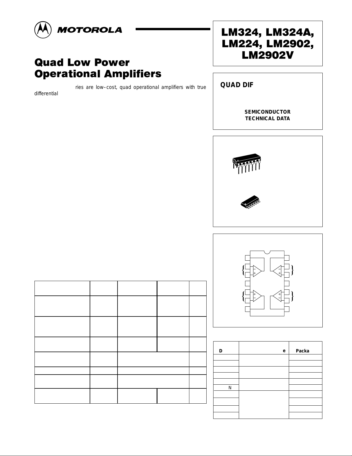
The LM324 series are low–cost, quad operational amplifiers with true
differential inputs. They have several distinct advantages over standard
operational amplifier types in single supply applications. The quad amplifier
can operate at supply voltages as low as 3.0 V or as high as 32 V with
quiescent currents about one–fifth of those associated with the MC1741 (on
a per amplifier basis). The common mode input range includes the negative
supply, thereby eliminating the necessity for external biasing components in
many applications. The output voltage range also includes the negative
power supply voltage.
• Short Circuited Protected Outputs
• True Differential Input Stage
• Single Supply Operation: 3.0 V to 32 V
• Low Input Bias Currents: 100 nA Maximum (LM324A)
• Four Amplifiers Per Package
• Internally Compensated
• Common Mode Range Extends to Negative Supply
• Industry Standard Pinouts
• ESD Clamps on the Inputs Increase Ruggedness without Af fecting
Device Operation
QUAD DIFFERENTIAL INPUT
OPERATIONAL AMPLIFIERS
SEMICONDUCTOR
TECHNICAL DATA
N SUFFIX
PLASTIC PACKAGE
14
1
14
1
PIN CONNECTIONS
CASE 646
(LM224, LM324,
LM2902 Only)
D SUFFIX
PLASTIC PACKAGE
CASE 751A
(SO–14)
MAXIMUM RATINGS
Rating Symbol
Power Supply Voltages Vdc
Single Supply V
Split Supplies VCC, V
Input Differential
Voltage Range (See
Note 1)
Input Common Mode
Voltage Range
Output Short Circuit
Duration
Junction Temperature T
Storage Temperature
Range
Operating Ambient
T emperature Range
NOTE: 1. Split Power Supplies.
(TA = +25°C, unless otherwise noted.)
LM224
LM324, LM324A
32 26
±16 ±13
±32 ±26 Vdc
–0.3 to 32 –0.3 to 26 Vdc
Continuous
150 °C
–65 to +150 °C
–25 to +85
0 to +70
–40 to +105
–40 to +125
V
V
IDR
ICR
t
SC
T
T
CC
EE
J
stg
A
LM2902,
LM2902V
Unit
°C
Inputs 1
Inputs 2
Device
LM2902D
LM2902N
LM2902VD
LM2902VN
LM224D
LM224N
LM324AD
LM324AN
LM324D
LM324N
Out 1
V
CC
Out 2
1
2
*
1
)
3
4
5
)
23
*
6
7
(Top View)
14
13
*
4
)
12
11
10
)
*
9
8
Out 4
Inputs 4
VEE, Gnd
Inputs 3
Out 3
ORDERING INFORMATION
Operating
Temperature Range
TA = –40° to +105°C
TA = –40° to +125°C
TA = –25° to +85°C
TA = 0° to +70°C
Package
Plastic DIP
Plastic DIP
Plastic DIP
Plastic DIP
Plastic DIP
SO–14
SO–14
SO–14
SO–14
SO–14
MOTOROLA ANALOG IC DEVICE DATA
Motorola, Inc. 1996 Rev 3
1

LM324, LM324A, LM224, LM2902, LM2902V
ELECTRICAL CHARACTERISTICS
Characteristics Symbol Min Typ Max Min Typ Max Min Typ Max Min Typ Max Min Typ Max Unit
Input Offset Voltage V
VCC = 5.0 V to 30 V
(26 V for LM2902,
V), V
= 0 V to
ICR
VCC –1.7 V, VO =
1.4 V, RS = 0 Ω
TA = 25°C
TA = T
TA = T
Average Temperature
Coefficient of Input
Offset Voltage
TA = T
high
Input Offset Current I
TA = T
high
Average Temperature
Coefficient of Input
Offset Current
TA = T
high
Input Bias Current I
TA = T
high
Input Common Mode
Voltage Range
VCC = 30 V (26 V for
LM2902, V)
VCC = 30 V (26 V for
LM2902, V),
TA = T
Differential Input
Voltage Range
Large Signal Open
Loop Voltage Gain
RL = 2.0 kΩ, VCC =
15 V, for Large V
Swing, TA = T
to T
low
Channel Separation
10 kHz ≤ f ≤ 20 kHz,
Input Referenced
Common Mode
Rejection, RS ≤ 10 kΩ
Power Supply
Rejection
Output Voltage–High
Limit (TA = T
(1)
T
)
low
VCC = 5.0 V, RL =
2.0 kΩ, TA = 25°C
VCC = 30 V (26 V for
LM2902, V),
RL = 2.0 kΩ
VCC = 30 V (26 V for
LM2902, V),
RL = 10 kΩ
NOTES: 1. T
2.The input common mode voltage or either input signal voltage should not be allowed to go negative by more than 0.3 V. The upper end of the
(1)
high
(1)
low
to T
low
to T
low
to T
low
to T
low
(2)
to T
high
high
(1)
high to
= –25°C for LM224 T
low
=0°C for LM324, A = +70°C for LM324, A
= –40°C for LM2902 = +105°C for LM2902
= –40°C for LM2902V = +125°C for LM2902V
common mode voltage range is VCC –1.7 V.
IO
∆VIO/∆T – 7.0 – – 7.0 30 – 7.0 – – 7.0 – – 7.0 – µV/°C
(1)
IO
(1)
∆IIO/∆T – 10 – – 10 300 – 10 – – 10 – – 10 – pA/°C
(1)
IB
(1)
V
ICR
low
V
IDR
A
VOL
O
CS – –120 – – –120 – – –120 – – –120 – – –120 – dB
CMR 70 85 – 65 70 – 65 70 – 50 70 – 50 70 – dB
PSR 65 100 – 65 100 – 65 100 – 50 100 – 50 100 – dB
V
OH
(VCC = 5.0 V, VEE = Gnd, TA = 25°C, unless otherwise noted.)
LM224 LM324A LM324 LM2902 LM2902V
– 2.0 5.0 – 2.0 3.0 – 2.0 7.0 – 2.0 7.0 – 2.0 7.0
– – 7.0 – – 5.0 – – 9.0 – – 10 – – 13
– – 7.0 – – 5.0 – – 9.0 – – 10 – – 10
– 3.0 30 – 5.0 30 – 5.0 50 – 5.0 50 – 5.0 50 nA
– – 100 – – 75 – – 150 – – 200 – – 200
– –90 –150 – –45 –100 – –90 –250 – –90 –250 – –90 –250 nA
– – –300 – – –200 – – –500 – – –500 – – –500
0 – 28.3 0 – 28.3 0 – 28.3 0 – 24.3 0 – 24.3
0 – 28 0 – 28 0 – 28 0 – 24 0 – 24
– – V
5025100–––2515100–––2515100–––2515100–––2515100––
3.3 3.5 – 3.3 3.5 – 3.3 3.5 – 3.3 3.5 – 3.3 3.5 –
26 – – 26 – – 26 – – 22 – – 22 – –
27 28 – 27 28 – 27 28 – 23 24 – 23 24 –
= +85°C for LM224
high
CC
– – V
CC
– – V
CC
– – V
CC
– – V
CC
–
mV
V
V
V/mV
V
2
MOTOROLA ANALOG IC DEVICE DATA

LM324, LM324A, LM224, LM2902, LM2902V
ELECTRICAL CHARACTERISTICS (V
Characteristics Symbol Min Typ Max Min Typ Max Min Typ Max Min Typ Max Min Typ Max Unit
Output Voltage – Low
Limit, VCC = 5.0 V, R
= 10 kΩ, TA = T
T
low
Output Source Current
(VID = +1.0 V, VCC =
15 V)
TA = 25°C
TA = T
Output Sink Current IO
(VID = –1.0 V, VCC =
15 V) TA = 25°C
TA = T
(VID = –1.0 V, VO =
200 mV, TA = 25°C)
Output Short Circuit to
Ground
Power Supply Current
(TA = T
VCC = 30 V (26 V for
LM2902, V),
VO = 0 V, RL = ∞
VCC = 5.0 V,
VO = 0 V, RL = ∞
NOTES: 1. T
high
(1)
to T
high
low
to T
high
low
(3)
to T
high
low
= –25°C for LM224 T
low
=0°C for LM324, A = +70°C for LM324, A
= –40°C for LM2902 = +105°C for LM2902
= –40°C for LM2902V = +125°C for LM2902V
2.The input common mode voltage or either input signal voltage should not be allowed to go negative by more than 0.3 V. The upper end of the
common mode voltage range is VCC –1.7 V.
V
L
to
IO
(1)
(1)
I
SC
I
CC
(1)
)
– 5.0 20 – 5.0 20 – 5.0 20 – 5.0 100 – 5.0 100 mV
OL
+
20 40 – 20 40 – 20 40 – 20 40 – 20 40 –
10 20 – 10 20 – 10 20 – 10 20 – 10 20 –
–
10 20 – 10 20 – 10 20 – 10 20 – 10 20 –
5.0 8.0 – 5.0 8.0 – 5.0 8.0 – 5.0 8.0 – 5.0 8.0 –
12 50 – 12 50 – 12 50 – – – – – – – µA
– 40 60 – 40 60 – 40 60 – 40 60 – 40 60 mA
– – 3.0 – 1.4 3.0 – – 3.0 – – 3.0 – – 3.0
– – 1.2 – 0.7 1.2 – – 1.2 – – 1.2 – – 1.2
= 5.0 V, VEE = Gnd, TA = 25°C, unless otherwise noted.)
CC
LM224 LM324A LM324 LM2902 LM2902V
= +85°C for LM224
high
mA
mA
mA
+
Inputs
–
Q2
Q19
Q18
Q17
Q3 Q4
5.0 pF
Q20
Q21
Q16
Q5
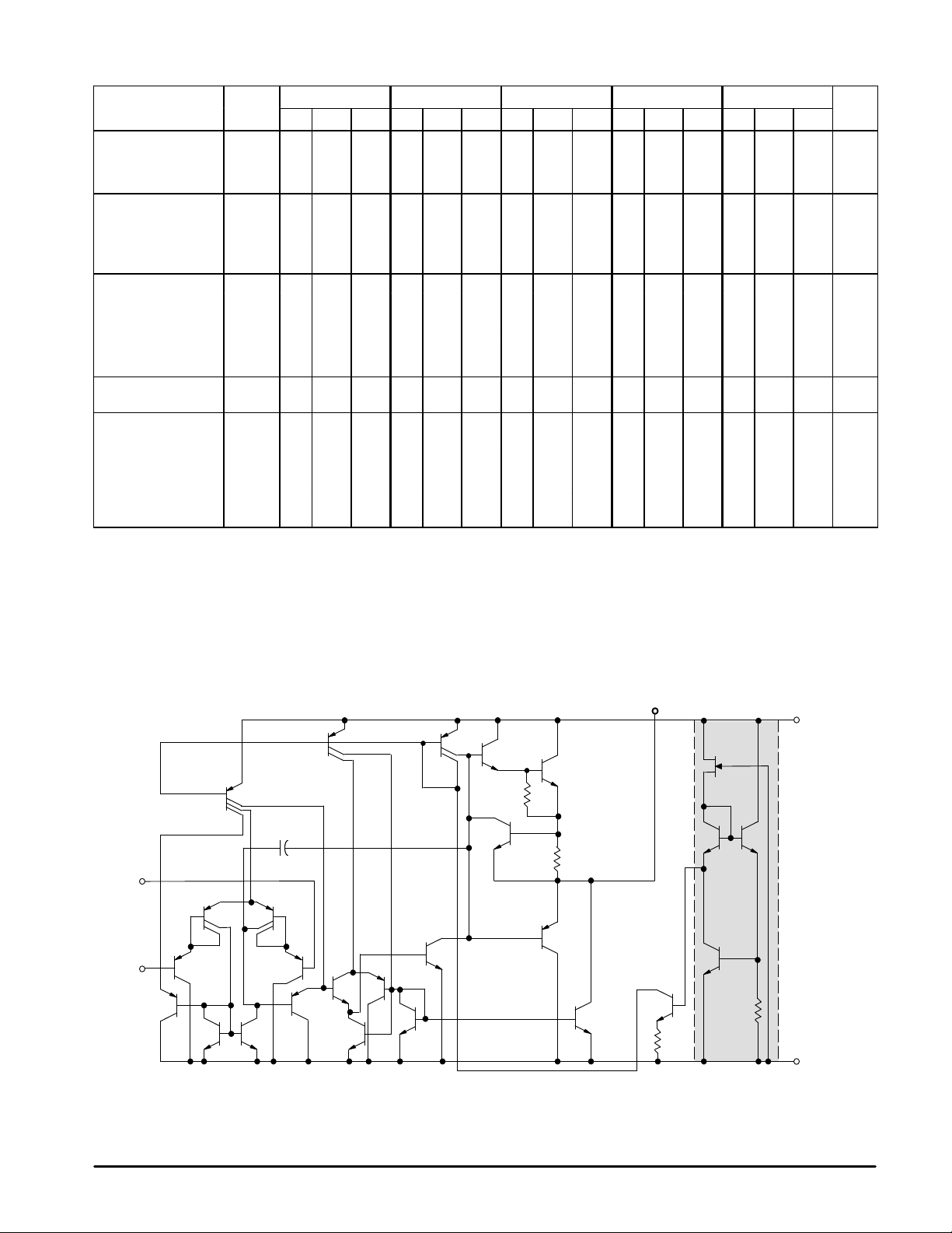
Representative Circuit Diagram
(One–Fourth of Circuit Shown)
Q15
Q12
Q9
Q7
Q6
Q26
Q8
Q14
40 k
25
Q13
Q11
Q10
Output
Q1
Bias Circuitry
Common to Four
Amplifiers
Q22
Q23
Q25
2.0 k
2.4 k
Q24
V
CC
VEE/Gnd
MOTOROLA ANALOG IC DEVICE DATA
3
 Loading...