

Page 1

查询68HC05J5A供应商
HC05J5AGRS/H
REV 2.1
68HC05J5A
68HRC05J5A
68HC705J5A
68HRC705J5A
SPECIFICATION
(General Release)
July 16, 1999
Semiconductor Products Sector
Motorola reserves the right to make changes without further notice to any products herein
to improve reliability, function or design. Motorola does not assume any liability arising out
of the application or use of any product or circuit described herein; neither does it convey
any license under its patent rights nor the rights of others. Motorola products are not
designed, intended, or authorized for use as components in systems intended for surgical
implant into the body, or other applications intended to support or sustain life, or for any
other application in which the failure of the Motorola product could create a situation
where personal injury or death may occur. Should Buyer purchase or use Motorola
products for any such unintended or unauthorized application, Buyer shall indemnify and
hold Motorola and its officers, employees, subsidiaries, affiliates, and distributors
harmless against all claims, costs, damages, and expenses, and reasonable attorney
fees arising out of, directly or indirectly, any claim of personal injury or death associated
with such unintended or unauthorized use, even if such claim alleges that Motorola was
negligent regarding the design or manufacture of the part.
Motorola, Inc., 1999
Page 2

Page 3

July 16, 1999 GENERAL RELEASE SPECIFICATION
TABLE OF CONTENTS
Section Page
SECTION 1
GENERAL DESCRIPTION
1.1 FEATURES...................................................................................................... 1-1
1.2 MASK OPTIONS..............................................................................................1-2
1.3 MCU STRUCTURE..........................................................................................1-2
1.4 PIN ASSIGNMENTS........................................................................................ 1-4
1.5 FUNCTIONAL PIN DESCRIPTION..................................................................1-4
1.5.1 V
AND V
DD
..............................................................................................1-4
SS
1.5.2 OSC1, OSC2/R............................................................................................1-4
1.5.3 RESET
1.5.4 IRQ
.........................................................................................................1-6
(MASKABLE INTERRUPT REQUEST)................................................1-6
1.5.5 PA0-PA7......................................................................................................1-6
1.5.6 PB0-PB5......................................................................................................1-7
SECTION 2
MEMORY
2.1 I/O AND CONTROL REGISTERS ...................................................................2-2
2.2 RAM.................................................................................................................2-2
2.3 ROM.................................................................................................................2-2
2.4 I/O REGISTERS SUMMARY...........................................................................2-3
SECTION 3
CENTRAL PROCESSING UNIT
3.1 REGISTERS ....................................................................................................3-1
3.2 ACCUMULATOR (A)........................................................................................3-2
3.3 INDEX REGISTER (X)..................................................................................... 3-2
3.4 STACK POINTER (SP).................................................................................... 3-2
3.5 PROGRAM COUNTER (PC) ...........................................................................3-2
3.6 CONDITION CODE REGISTER (CCR)...........................................................3-3
3.6.1 Half Carry Bit (H-Bit)....................................................................................3-3
3.6.2 Interrupt Mask (I-Bit)....................................................................................3-3
3.6.3 Negative Bit (N-Bit)......................................................................................3-3
3.6.4 Zero Bit (Z-Bit).............................................................................................3-3
3.6.5 Carry/Borrow Bit (C-Bit)...............................................................................3-4
SECTION 4
INTERRUPTS
4.1 CPU INTERRUPT PROCESSING...................................................................4-1
4.2 RESET INTERRUPT SEQUENCE ..................................................................4-2
4.3 SOFTWARE INTERRUPT (SWI).....................................................................4-3
4.4 HARDWARE INTERRUPTS............................................................................4-3
4.5 EXTERNAL INTERRUPT (IRQ).......................................................................4-3
4.5.1 IRQ CONTROL/STATUS REGISTER (ICSR) $0A......................................4-5
MC68HC05J5A MOTOROLA
REV 2.1 i
Page 4

GENERAL RELEASE SPECIFICATION July 16, 1999
TABLE OF CONTENTS
Section Page
4.5.2 OPTIONAL EXTERNAL INTERRUPTS (PA0-PA3) ....................................4-6
4.5.3 TIMER INTERRUPT (MFT).........................................................................4-7
4.5.4 TIMER1 INTERRUPT (16-BIT TIMER)........................................................4-7
SECTION 5
RESETS
5.1 EXTERNAL RESET (RESET)..........................................................................5-2
5.2 INTERNAL RESETS........................................................................................ 5-2
5.2.1 POWER-ON RESET (POR) ........................................................................5-2
5.2.2 COMPUTER OPERATING PROPERLY RESET (COPR)...........................5-2
5.2.3 LOW VOLTAGE RESET (LVR)...................................................................5-3
5.2.4 ILLEGAL ADDRESS RESET (ILADR).........................................................5-3
SECTION 6
LOW POWER MODES
6.1 STOP INSTRUCTION......................................................................................6-2
6.1.1 STOP Mode.................................................................................................6-3
6.1.2 HALT Mode..................................................................................................6-3
6.2 WAIT INSTRUCTION.......................................................................................6-4
6.3 DATA-RETENTION MODE..............................................................................6-4
6.4 COP WATCHDOG TIMER CONSIDERATIONS .............................................6-4
SECTION 7
INPUT/OUTPUT PORTS
7.1 SLOW OUTPUT FALLING-EDGE TRANSITION.............................................7-1
7.2 PORT A............................................................................................................7-1
7.2.1 Port A Data Register....................................................................................7-2
7.2.2 Port A Data Direction Register.....................................................................7-2
7.2.3 Port A Pulldown/up Register........................................................................7-3
7.2.4 Port A Drive Capability.................................................................................7-3
7.2.5 Port A I/O Pin Interrupts...............................................................................7-3
7.3 PORT B............................................................................................................7-4
7.3.1 Port B Data Register....................................................................................7-4
7.3.2 Port B Data Direction Register.....................................................................7-5
7.3.3 Port B Pulldown/up Register........................................................................7-5
7.4 I/O PORT PROGRAMMING ............................................................................7-6
7.4.1 Pin Data Direction........................................................................................7-6
7.4.2 Output Pin....................................................................................................7-6
7.4.3 Input Pin.......................................................................................................7-6
7.4.4 I/O Pin Transitions.......................................................................................7-7
7.4.5 I/O Pin Truth Tables.....................................................................................7-7
MOTOROLA MC68HC05J5A
ii REV 2.1
Page 5

July 16, 1999 GENERAL RELEASE SPECIFICATION
TABLE OF CONTENTS
Section Page
SECTION 8
MULTI-FUNCTION TIMER
8.1 OVERVIEW......................................................................................................8-2
8.2 COMPUTER OPERATING PROPERLY (COP) WATCHDOG........................8-2
8.3 MFT REGISTERS............................................................................................ 8-2
8.3.1 Timer Counter Register (TCR) $09..............................................................8-3
8.3.2 Timer Control/Status Register (TCSR) $08.................................................8-3
8.4 OPERATION DURING STOP MODE..............................................................8-5
8.5 OPERATION DURING WAIT/HALT MODE.....................................................8-5
SECTION 9
16-BIT TIMER
9.1 TIMER1 COUNTER REGISTERS (TCNTH, TCNTL)......................................9-2
9.2 ALTERNATE COUNTER REGISTERS (ACNTH, ACNTL)..............................9-3
9.3 INPUT CAPTURE REGISTERS ......................................................................9-5
9.4 TIMER1 CONTROL REGISTER (T1CR).........................................................9-8
9.5 TIMER1 STATUS REGISTER (T1SR).............................................................9-9
9.6 TIMER1 OPERATION DURING WAIT MODE.................................................9-9
9.7 TIMER1 OPERATION DURING STOP MODE................................................9-9
SECTION 10
INSTRUCTION SET
10.1 ADDRESSING MODES.................................................................................10-1
10.1.1 Inherent......................................................................................................10-1
10.1.2 Immediate..................................................................................................10-1
10.1.3 Direct .........................................................................................................10-2
10.1.4 Extended....................................................................................................10-2
10.1.5 Indexed, No Offset.....................................................................................10-2
10.1.6 Indexed, 8-Bit Offset..................................................................................10-2
10.1.7 Indexed, 16-Bit Offset................................................................................10-3
10.1.8 Relative......................................................................................................10-3
10.1.9 Instruction Types .......................................................................................10-3
10.1.10 Register/Memory Instructions....................................................................10-4
10.1.11 Read-Modify-Write Instructions .................................................................10-5
10.1.12 Jump/Branch Instructions..........................................................................10-5
10.1.13 Bit Manipulation Instructions......................................................................10-7
10.1.14 Control Instructions....................................................................................10-7
10.1.15 Instruction Set Summary ...........................................................................10-8
MC68HC05J5A MOTOROLA
REV 2.1 iii
Page 6

GENERAL RELEASE SPECIFICATION July 16, 1999
TABLE OF CONTENTS
Section Page
SECTION 11
ELECTRICAL SPECIFICATIONS
11.1 MAXIMUM RATINGS.....................................................................................11-1
11.2 THERMAL CHARACTERISTICS...................................................................11-1
11.3 FUNCTIONAL OPERATING RANGE............................................................11-1
11.4 DC ELECTRICAL CHARACTERISTICS........................................................11-2
11.5 CONTROL TIMING........................................................................................11-5
SECTION 12
MECHANICAL SPECIFICATIONS
12.1 16-PIN PDIP (CASE #648) ............................................................................12-1
12.2 16-PIN SOIC (CASE #751G).........................................................................12-1
12.3 20-PIN PDIP (CASE #738) ............................................................................12-2
12.4 20-PIN SOIC (CASE #751D) .........................................................................12-2
APPENDIX A
MC68HRC05J5A
A.1 INTRODUCTION..............................................................................................A-1
A.2 RC OSCILLATOR CONNECTIONS.................................................................A-1
A.3 ELECTRICAL CHARACTERISTICS................................................................A-2
APPENDIX B
MC68HC705J5A
B.1 INTRODUCTION..............................................................................................B-1
B.2 MEMORY.........................................................................................................B-1
B.3 MASK OPTION REGISTERS (MOR)...............................................................B-1
B.4 BOOTSTRAP MODE.......................................................................................B-4
B.5 EPROM PROGRAMMING...............................................................................B-4
B.5.1 EPROM Program Control Register (PCR)...................................................B-4
B.5.2 Programming Sequence..............................................................................B-5
B.6 ELECTRICAL CHARACTERISTICS................................................................B-6
APPENDIX C
MC68HRC705J5A
C.1 INTRODUCTION..............................................................................................C-1
C.2 RC OSCILLATOR CONNECTIONS.................................................................C-1
C.3 ELECTRICAL CHARACTERISTICS................................................................C-2
APPENDIX D
ORDERING INFORMATION
D.1 MC ORDER NUMBERS...................................................................................D-1
MOTOROLA MC68HC05J5A
iv REV 2.1
Page 7

July 16, 1999 GENERAL RELEASE SPECIFICATION
LIST OF FIGURES
Figure Title Page
1-1 MC68HC05J5A Block Diagram........................................................................1-3
1-2 Pin Assignments for 16-Pin and 20-Pin Packages...........................................1-4
1-3 Oscillator Connections..................................................................................... 1-5
2-1 MC68HC05J5A Memory Map..........................................................................2-1
2-2 I/O Registers Memory Map..............................................................................2-2
2-3 I/O Registers $0000-$000F..............................................................................2-3
2-4 I/O Registers $0010-$001F..............................................................................2-4
3-1 MC68HC05 Programming Model.....................................................................3-1
4-1 Interrupt Processing Flowchart........................................................................4-2
4-2 IRQ Function Block Diagram............................................................................4-3
4-3 IRQ Status & Control Register......................................................................... 4-5
5-1 Reset Block Diagram.......................................................................................5-1
6-1 STOP/HALT/WAIT Flowcharts.........................................................................6-2
7-1 Port B Data Direction Register.........................................................................7-1
7-2 Port A I/O Circuitry...........................................................................................7-2
7-3 Port B I/O Circuitry...........................................................................................7-4
8-1 Multi-Function Timer Block Diagram................................................................8-1
8-2 COP Watchdog Timer Location.......................................................................8-2
8-3 Timer Counter Register....................................................................................8-3
8-4 Timer Control/Status Register (TCSR).............................................................8-3
9-1 16-Bit Timer Block Diagram.............................................................................9-1
9-2 16-Bit Timer Counter Block Diagram...............................................................9-2
9-3 16-Bit Timer Counter Registers (TCNTH, TCNTL)..........................................9-3
9-4 Alternate Counter Block Diagram.....................................................................9-4
9-5 Alternate Counter Registers (ACNTH, ACNTL)...............................................9-4
9-6 Timer Input Capture Block Diagram.................................................................9-5
9-7 Timer1 Capture Control Register.....................................................................9-6
9-8 TCAP Input Signal Conditioning.......................................................................9-6
9-9 TCAP Input Comparator Output.......................................................................9-7
9-10 Input Capture Registers (ICH, ICL)..................................................................9-7
9-11 Timer Control Register (T1CR)........................................................................9-8
9-12 Timer Status Registers (T1SR)........................................................................9-9
12-1 16-Pin PDIP Mechanical Dimensions............................................................12-1
12-2 16-Pin SOIC Mechanical Dimensions............................................................12-1
12-3 20-Pin PDIP Mechanical Dimensions............................................................12-2
12-4 20-Pin SOIC Mechanical Dimensions............................................................12-2
A-1 RC Oscillator Connections...............................................................................A-1
A-2 Typical Internal Operating Frequency for RC Oscillator Connections..............A-2
B-1 MC68HC705J5A Memory Map........................................................................B-3
B-2 EPROM Programming Sequence....................................................................B-5
C-1 RC Oscillator Connections...............................................................................C-1
C-2 Typical Internal Operating Frequency for RC Oscillator Connections..............C-2
MC68HC05J5A MOTOROLA
REV 2.1 v
Page 8

GENERAL RELEASE SPECIFICATION July 16, 1999
LIST OF FIGURES
Figure Title Page
MOTOROLA MC68HC05J5A
vi REV 2.1
Page 9

July 16, 1999 GENERAL RELEASE SPECIFICATION
LIST OF TABLES
Table Title Page
4-1 Vector Address for Interrupts and Reset..........................................................4-1
6-1 COP Watchdog Timer Recommendations.......................................................6-5
7-1 Port A I/O Pin Functions...................................................................................7-7
7-2 Port B I/O Pin Functions...................................................................................7-7
8-1 RTI Rates and COP Reset Times....................................................................8-5
10-1 Register/Memory Instructions........................................................................10-4
10-2 Read-Modify-Write Instructions .....................................................................10-5
10-3 Jump and Branch Instructions........................................................................10-6
10-4 Bit Manipulation Instructions.......................................................................... 10-7
10-5 Control Instructions........................................................................................ 10-7
10-6 Instruction Set Summary ...............................................................................10-8
10-7 Opcode Map.................................................................................................10-14
11-1 DC Electrical Characteristics, VDD=5 V ........................................................11-2
11-2 DC Electrical Characteristics, VDD=2.2V .....................................................11-3
11-3 Control Timing, VDD=5V...............................................................................11-5
11-4 Control Timing, VDD=2.2V............................................................................11-5
A-1 Functional Operating Range............................................................................A-2
A-2 DC Electrical Characteristics, VDD=5V...........................................................A-2
B-1 Functional Operating Range............................................................................B-6
B-2 EPROM Programming Electrical Characteristics.............................................B-6
B-3 DC Electrical Characteristics, VDD=5V..........................................................B-6
C-1 Functional Operating Range............................................................................C-2
C-2 DC Electrical Characteristics, VDD=5V..........................................................C-2
D-1 MC Order Numbers..........................................................................................D-1
MC68HC05J5A MOTOROLA
REV 2.1 vii
Page 10

GENERAL RELEASE SPECIFICATION July 16, 1999
LIST OF TABLES
Table Title Page
MOTOROLA MC68HC05J5A
viii REV 2.1
Page 11

July 16, 1999 GENERAL RELEASE SPECIFICATION
SECTION 1
GENERAL DESCRIPTION
The MC68HC05J5A is a member of the low-cost high-performance M68HC05
Family of 8-bit microcontroller units (MCUs). The M68HC05 Family is based on
the customer-specified integrated circuit design strategy. All MCUs in the family
use the popular M68HC05 central processing unit (CPU) and are available with a
variety of subsystems, memory sizes and types, and package types.
The MC68HC05J5A is an enhanced version of the MC68HC05J5, with expanded
RAM, ROM sizes, and an additional 16-bit timer with TCAP. This MCU is available
in 20-pin PDIP, 20-pin SOIC, 16-pin PDIP, and 16-pin SOIC packages. The 16-pin
version has four less I/O lines.
Three variation on the MC68HC05J5A device are available; a summary of their
differences are listed in the following table:
DEVICE ROM TYPE OSCILLATOR OPTION REFERENCE
MC68HC05J5A 2560 bytes ROM Crystal/resonator or external clock oscillator —
MC68HRC05J5A 2560 bytes ROM RC oscillator
MC68HC705J5A 2560 bytes EPROM Crystal/resonator or external clock oscillator
MC68HRC705J5A 2560 bytes EPROM RC oscillator
Appendix A
Appendix B
Appendix C
1.1 FEATURES
The features of the MC68HC05J5A include the following:
• Industry standard M68HC05 CPU core
• Fully static operation with no minimum clock speed
• Power-saving STOP and WAIT modes
• Memory-Mapped Input/Output (I/O) registers
• 2560 Bytes of user ROM with security feature
• 128 Bytes of user RAM
• On-Chip Oscillator:
– Crystal/Resonator oscillator
– External clock oscillator
• 15-Bit Multi-function Timer
• 16-Bit Programmable Timer with Input Capture
MC68HC05J5A
REV 2.1 1-1
GENERAL DESCRIPTION
MOTOROLA
Page 12

GENERAL RELEASE SPECIFICATION July 16, 1999
• 14 Bidirectional I/O pins (10 I/O pins on 16-pin package)
– PA0-PA5, PB0, and PB3-PB5: with software programmable input pull-
down devices
– PB1, PB2, PA6 and PA7: open-drained I/O pins with software
programmable pull-up devices
– PA6, PA7, and PB1: with slow output falling transition feature
– PA7: with falling-edge interrupt capability
– PA0-PA3: with maskable rising-edge only or rising-edge and high
level interrupt capability
– 20-pin package: PB1 and PB2, each with 25mA current sink
capability
– 16-pin package: PB1 with 50mA current sink capability
• Computer Operation Properly (COP) Watchdog
• Low Voltage Reset Circuit
• Illegal Address Reset
• 20-pin PDIP, 20-pin SOIC, 16-pin PDIP, and 16-pin SOIC packages
1.2 MASK OPTIONS
The following mask options are available on the MC68HC05J5A:
STOP instruction convert to WAIT [Enabled] or [Disabled]
External interrupt pins (IRQ, PA0-PA3) [Edge-triggered] or [Edge and level triggered]
Port A and Port B pull-down/pull-up resistors [Enabled] or [Disabled]
PA0-PA3 external interrupt capability [Enabled] or [Disabled]
Oscillator Delay Option (internal clock cycles) [224] or [4064]
Low Voltage Reset [Enabled] or [Disabled]
COP Watchdog Timer [Enabled] or [Disabled]
MASK OPTION
1.3 MCU STRUCTURE
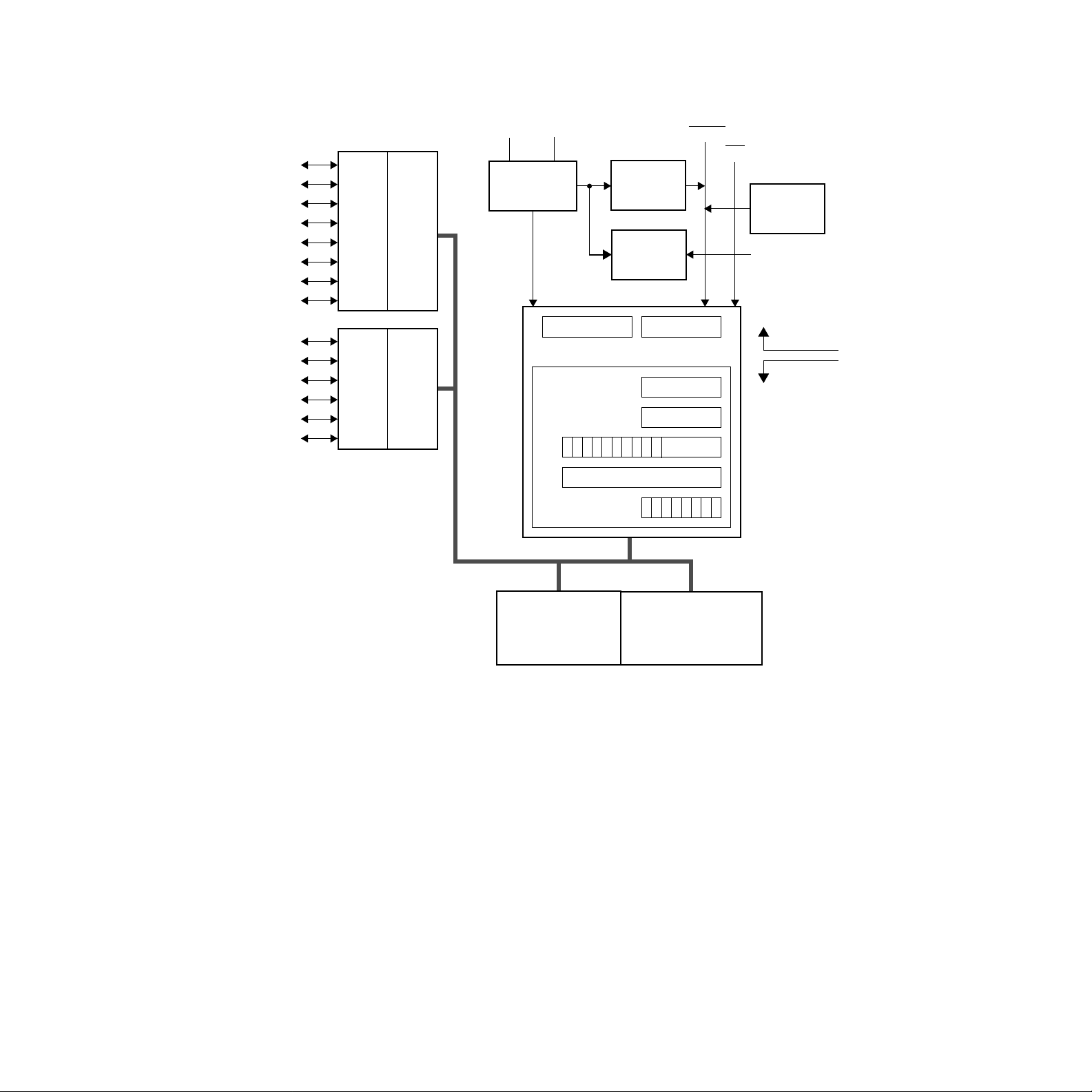
Figure 1-1 shows the structure of MC68HC05J5A MCU.
MOTOROLA
1-2 REV 2.1
GENERAL DESCRIPTION
MC68HC05J5A
Page 13
July 16, 1999 GENERAL RELEASE SPECIFICATION
PA0①
PA1①
PA2①
PA3①
PA4②
PA5②
PA6③
PA7④
PB0⑤
PB1⑥
PB2⑥⑦
PB3⑦
PB4⑦
PB5⑦
①
: External edge interrupt capability
②
: 8 mA current sink
③
: Open-drained with internal pull-up and
8 mA current sink
④
: External interrupt capability, open-drained
with internal pull-up and 8 mA current sink
⑤
: Shared pin: PB0/TCAP
⑥
: 25 mA current sink open-drained with
internal pull-up
⑦
: not bonded out in 16-pin package
PORT
REG
PORT
REG
DATA
A
B
DIR
REG
DATA
DIR
REG
OSC1
OSC2/R
OSCILLATOR
AND DIVIDE
BY 2
COND CODE REG 1 1 1 I N Z CH
2560 BYTES
CPU CONTROL
68HC05 CPU
CPU REGISERS
0 0 0 1100000
PROGRAM COUNTER
ROM
CORE
TIMER
(COP)
16-BIT
TIMER
INDEX REG
RESET
IRQ
LOW
VOLTAGE
RESET
TCAP⑤
ALU
VDD
VSS
ACCUM
STK PTR
128 BYTES
RAM
Figure 1-1. MC68HC05J5A Block Diagram
MC68HC05J5A
REV 2.1 1-3
GENERAL DESCRIPTION
MOTOROLA
Page 14
GENERAL RELEASE SPECIFICATION July 16, 1999
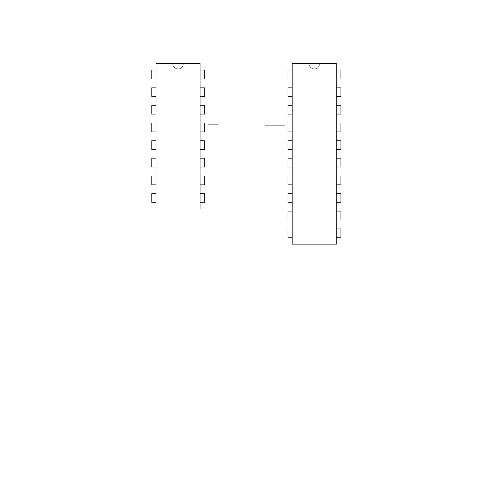
1.4 PIN ASSIGNMENTS
OSC2/R
OSC1
RESET
PA7
PA6
PA5
PA4
PB0/TCAP
IRQ/VPP: VPP is only available on EPROM parts
1
2
3
4
5
6
7
8
16
15
14
13
12
11
10
PB1
VDD
VSS
/VPP
IRQ
PA0
PA1
PA2
9
PA3
PB3
OSC2/R
OSC1
RESET
PA7
PA6
PA5
PA4
PB0/TCAP
PB4
1
2
3
4
5
6
7
8
9
20
19
18
17
16
15
14
13
12
1110
PB2
PB1
VDD
VSS
IRQ/VPP
PA0
PA1
PA2
PA3
PB5
Figure 1-2. Pin Assignments for 16-Pin and 20-Pin Packages
1.5 FUNCTIONAL PIN DESCRIPTION
The following paragraphs give a description of the general function of each pin
assigned in Figure 1-2 .
1.5.1 V
AND V
DD
SS
Power is supplied to the MCU through V
and V
is ground. The MCU operates from a single power supply.
SS
Very fast signal transitions occur on the MCU pins. The short rise and fall times
place very high short-duration current demands on the power supply. To prevent
noise problems, special care should be taken to provide good power supply
bypassing at the MCU by using b ypass capacitors with good high-frequency characteristics that are positioned as close to the MCU as possible. Bypassing
requirements vary, depending on how heavily the MCU pins are loaded.
1.5.2 OSC1, OSC2/R
The OSC1 and OSC2/R pins are the connections for the on-chip oscillator. The
OSC1 and OSC2/R pins can accept the following sets of components:
and V
DD
SS
. V
is the positive supply,
DD
MOTOROLA
1-4 REV 2.1
GENERAL DESCRIPTION
MC68HC05J5A
Page 15
.
July 16, 1999 GENERAL RELEASE SPECIFICATION
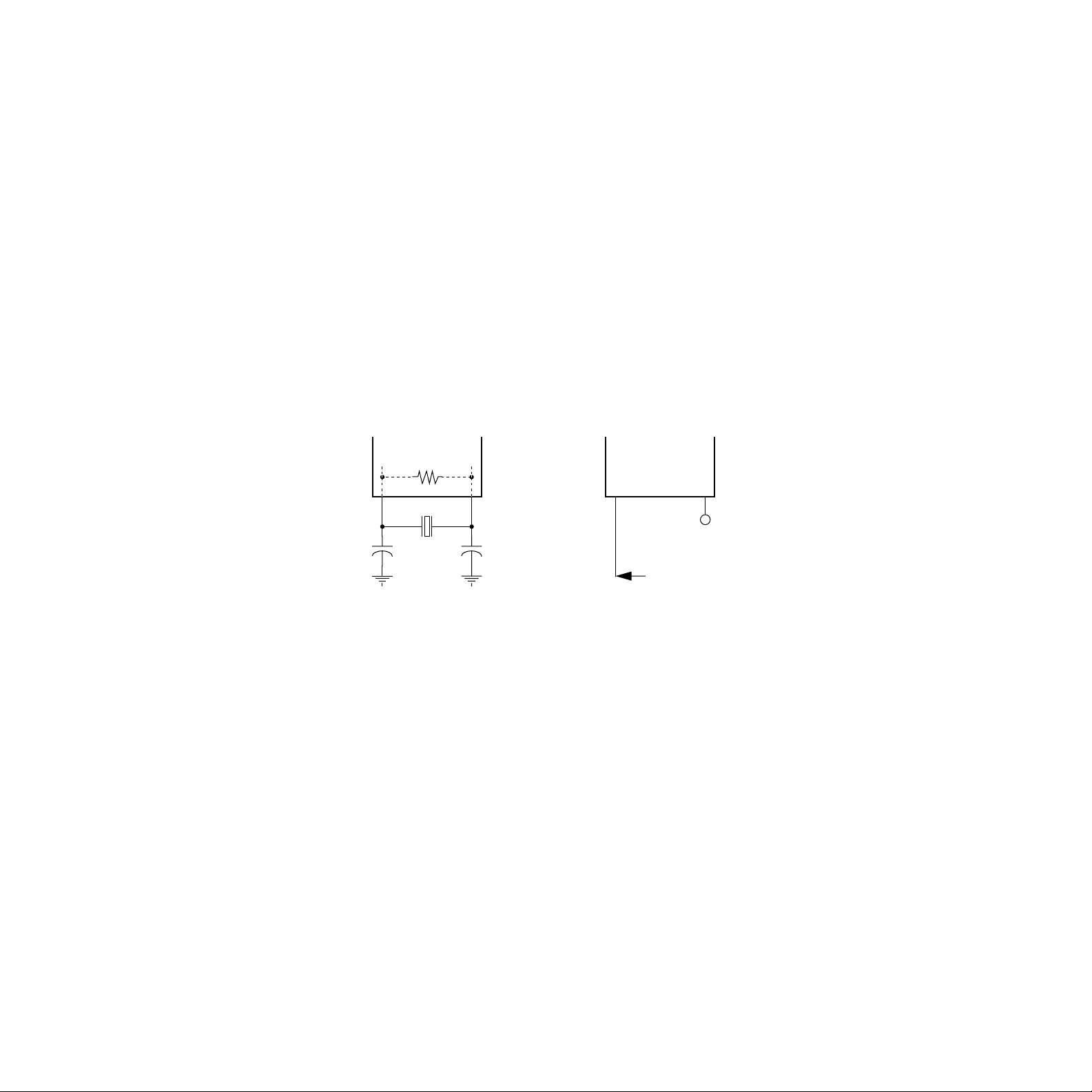
1. A crystal as shown in Figure 1-3 (a)
2. A ceramic resonator as shown in Figure 1-3 (a)
3. An external clock signal as shown in Figure 1-3 (b)
The frequency, f
produce the internal operating frequency, f
, of the oscillator or external clock source is divided by two to
OSC
OP
Crystal Oscillator
The circuit in Figure 1-3 (a) shows a typical oscillator circuit for an AT-cut, parallel
resonant crystal. The crystal manufacturer’s recommendations should be followed, as the crystal parameters determine the external component values
required to provide maximum stability and reliable start-up. The load capacitance
values used in the oscillator circuit design should include all stray capacitances.
The crystal and components should be mounted as close as possible to the pins
for start-up stabilization and to minimize output distortion. An internal start-up
resistor is provided between OSC1 and OSC2/R for the crystal type oscillator.
OSC1
37 pF
MCU
R
OSC
OSC2/R
37pF
OSC1
MCU
OSC2/R
unconnected
External Clock
(a) Crystal or ceramic
resonator connection
R
: see Section 11. Electrical Specifications.
OSC
(b) External clock source
connection
Figure 1-3. Oscillator Connections
Ceramic Resonator Oscillator
In cost-sensitive applications, a ceramic resonator can be used in place of the
crystal. The circuit in Figure 1-3 (a) can be used for a ceramic resonator. The resonator manufacturer’s recommendations should be followed, as the resonator
parameters determine the external component values required for maximum stability and reliable starting. The load capacitance values used in the oscillator circuit design should include all stray capacitances. The ceramic resonator and
components should be mounted as close as possible to the pins for start-up stabilization and to minimize output distortion. An internal start-up resistor is provided
between OSC1 and OSC2/R for the ceramic resonator type oscillator.
External Clock
An external clock from another CMOS-compatible device can be connected to the
OSC1 input, with the OSC2/R input not connected, as shown in Figure 1-3 (b).
MC68HC05J5A
REV 2.1 1-5
GENERAL DESCRIPTION
MOTOROLA
Page 16

GENERAL RELEASE SPECIFICATION July 16, 1999
1.5.3 RESET
This is an I/O pin. This pin can be used as an input to reset the MCU to a known
start-up state by pulling it to the low state. The RESET pin contains a steering
diode to discharge any voltage on the pin to V
internal pull-up is also connected between this pin and V
, when the power is removed. An
DD
. The RESET
DD
pin contains an internal Schmitt trigger to improve its noise immunity as an input. This pin
is an output pin if LVR triggers an internal reset.
1.5.4 IRQ (MASKABLE INTERRUPT REQUEST)
This input pin drives the asynchronous IRQ interrupt function of the CPU. The IRQ
interrupt function has a mask option to provide either only negative edge-sensitive
triggering or both negative edge-sensitive and low level-sensitive triggering. If the
option is selected to include level-sensitive triggering, the IRQ
external resistor to V
for "wired-OR" operation, if desired. The IRQ
DD
input requires an
pin contains
an internal Schmitt trigger as part of its input to improve noise immunity.
Each of the PA0 through PA3 I/O pins may be connected as an OR function with
the IRQ interrupt function by a mask option. This capability allows keyboard scan
applications where the transitions or levels on the I/O pins will behave the same
as the IRQ
selected by a separate mask option for the IRQ
OR’ed to create the IRQ signal. Besides, PA7 also has falling-edge only interrupt
capability whose functionality is controlled by another set of register bits.
1.5.5 PA0-PA7
These eight I/O lines comprise Port A. PA6 and PA7 are open-drained pins with
pull-up devices whereas PA0 to PA5 are push-pull pins with pull-down devices.
PA4 to PA7 are also capable of sinking 8mA.
The state of any pin is software programmable and all Port A lines are configured
as inputs during power-on or reset. The lower four I/O pins (PA0 to PA3) can be
connected via an internal OR gate to the IRQ interrupt function enabled by a mask
option. Another independent interrupt source comes from the falling-edge on PA7.
PA7 interrupt source is associated with a second set of interrupt control/status
bits. All Port A pins except PA6 and PA7 have software programmable pull-down
devices also provided by a mask option. PA6 and PA7 pins have software
programmable pull-up devices also provided by the same mask option. Pull-up
devices on PA6 and PA7 once enabled are always enabled regardless of pin
direction configuration, unlike pull-down devices on PA0 to PA5 which are
activated only when these pins are configured as input pins.
pin, except for the inverted phase. The edge or level sensitivity
pin also applies to the I/O pins
PA6 and PA7 pins, when configured as output pins, also have slow output fallingedge transition feature to reduce EMI. The falling-edge transition time is set at
250 ns typical at a specified load of 500 pF, assuming the bus rate is 2 MHz. The
slow transition output feature of PA6 and PA7, along with that of PB1 and PB2,
MOTOROLA
1-6 REV 2.1
GENERAL DESCRIPTION
MC68HC05J5A
Page 17

July 16, 1999 GENERAL RELEASE SPECIFICATION
can be enabled or disabled by software. Both PA6 and PA7 pins have Schmitt
trigger input for better noise immunity. V
and V
IH
are specified at 2.4V and 0.8V,
IL
respectively.
The slow transition feature of PA6 and PA7 pins can be enabled or disabled by
software. Once enabled, slow transition feature is applied to both pins while in
output mode.
1.5.6 PB0-PB5
NOTE
I/O lines PB2 to PB5 are not available on the 16-pin package.
These six I/O lines comprise Port B. PB0, PB3 to PB5 are push-pull I/O lines with
pull-down resistor. PB1 and PB2 are open-drain I/O lines with pull-up resistor.
The state of any line is software programmable and is configured as an input
during power-on or reset. I/O lines PB1 and PB2 have software programmable
pull-up device, whereas PB0, PB3 to PB5 have software programmable pull-down
device, provided by mask option. Pull-up devices on PB1 and PB2 lines once
enabled are always enabled regardless of pin direction configuration; unlike pulldown devices on PB0, PB3-PB5 lines, which are activated only when the pin is
configured as input pin.
Similar to PA6 and PA7, PB1 also has a slow output falling transition feature when
configured as an output line. PB1 has 25mA sink capability at 0.5V V
OL
.
PB2 output is one clock cycle (250 ns if bus rate is 2MHz) late than other I/O pins
if slow output transition feature is enabled. PB2 has 25mA sink capability at 0.5V
.
V
OL
NOTE
For the 16-pin package, PB1 and PB2 are bonded to the same pin and is labelled
PB1. This PB1 pin has 50mA sink capability if PB1 and PB2 data register bits they
are written with the same value at the same write cycle. The falling transition time
of PB1 is set at 250ns typical at a specified load of 50pF, assuming that the bus
rate is 2MHz. The slow transition feature on this PB1 pin is longer than PB1 pin for
the 20-pin package.
NOTE
If Port Data Register PB1 and PB2 are not written with the same value, PB1 pin
on the 16-pin package will sink 25 mA only and the output transition time will be
shorter.
MC68HC05J5A
REV 2.1 1-7
GENERAL DESCRIPTION
MOTOROLA
Page 18

GENERAL RELEASE SPECIFICATION July 16, 1999
MOTOROLA
1-8 REV 2.1
GENERAL DESCRIPTION
MC68HC05J5A
Page 19

July 16, 1999 GENERAL RELEASE SPECIFICATION
SECTION 2
MEMORY
The MC68HC05J5A has 4K-bytes of addressable memory consisting 32 bytes of
I/O, 128 bytes of user RAM, and 2560 bytes of user ROM, as shown in
Figure 2-1.
$0000
$001F
$0020
$007F
$0080
$00FF
$0100
$02FF
$0300
$0CFF
$0D00
$0DFF
$0E00 3584
$0FEF
$0FF0
$0FF5
$0FF6
$0FFF
Internal Test & Vectors
I/O
32 Bytes
unimplemented
96 Bytes
User RAM 128 Bytes
Stack
unimplemented
512 Bytes
User ROM
2560 Bytes
unimplemented
256 Bytes
496 Bytes ROM
ROM Reserved
6 Bytes
User Vectors ROM
10 Bytes
0000
0031
0032
0127
0128
0192 $00C0
0255
0256
0767
0768
3327
3328
3583
4079
4080
4085
4086
4095
$0000
I/O
Registers
32 bytes
(see Figure 2-2)
$001F
COP Watchdog Timer*
Reserved
Reserved
Reserved
Reserved
Reserved
Timer1 Vector (High Byte)
Timer1 Vector (Low Byte)
MFT Vector (High Byte)
MFT Vector (Low Byte)
IRQ Vector (High Byte)
IRQ Vector (Low Byte)
SWI Vector (High Byte)
SWI Vector (Low Byte)
Reset Vector (High Byte)
Reset Vector (Low Byte)
* Writing a 0 to bit 0 of $0FF0 clears the COP Timer.
Reading $0FF0 returns ROM data.
$0FF0
$0FF1
$0FF2
$0FF3
$0FF4
$0FF5
$0FF6
$0FF7
$0FF8
$0FF9
$0FFA
$0FFB
$0FFC
$0FFD
$0FFE
$0FFF
Figure 2-1. MC68HC05J5A Memory Map
MC68HC05J5A
REV 2.1 2-1
MEMORY
MOTOROLA
Page 20

GENERAL RELEASE SPECIFICATION July 16, 1999
2.1 I/O AND CONTROL REGISTERS
The I/O and Control Registers reside in locations $0000-$001F. The overall organization of these registers is shown in Figure 2-2. The bit assignments for each
register are shown in Figure 2-3 and Figure 2-4. Reading from unimplemented
bits will return unknown states, and writing to unimplemented bits will be ignored.
Port A Data Register
Port B Data Register
Timer1 Capture Control Register
unimplemented (1)
Port A Data Direction Register
Port B Data Direction Register
unimplemented (2)
MFT Control & Status Register
MFT Counter Register
IRQ Control & Status Register
unimplemented (5)
Port A Pulldown/up Register
Port B Pulldown/up Register
Timer1 Registers (4)
unimplemented (2)
Timer1 Registers (4)
unimplemented (3)
Reserved
Reserved for Test
$0000
$0001
$0002
$0003
$0004
$0005
$0008
$0009
$000A
$0010
$0011
$0012
$0015
$0018
$001B
$001E
$001F
Figure 2-2. I/O Registers Memory Map
2.2 RAM
The total RAM consists of 128 bytes (including the stack) at locations $0080
through $00FF. The stack begins at address $00FF and proceeds down to $00C0.
Using the stack area for data stor age or tempor ary work locations requires care to
prevent it from being overwritten due to stacking from an interrupt or subroutine
call.
2.3 ROM
There are a total of 2570 bytes of user ROM on-chip. This includes 2560 bytes of
user ROM from locations $0300 to $0CFF for user program storage and 10 bytes
for user vectors from locations $0FF6 to $0FFF.
MOTOROLA MEMORY MC68HC05J5A
2-2 REV 2.1
Page 21

July 16, 1999 GENERAL RELEASE SPECIFICATION
2.4 I/O REGISTERS SUMMARY
ADDR REGISTER R/W BIT 7 BIT 6 BIT 5 BIT 4 BIT 3 BIT 2 BIT 1 BIT 0
$0000
$0001
$0002
$0003 Unimplemented
$0004
$0005
$0006
$0007 Unimplemented
$0008
$0009
$000A
$000B Unimplemented
$000C Unimplemented
$000D Unimplemented
$000E Unimplemented
$000F Unimplemented
Port A Data R
PORTA W
Port B Data R 0 0
PORTB W
Timer1 Capture Control
T1CC W
Port A Data Direction R
DDRA W
Port B Data Direction R
DDRB W
Unimplemented
MFT Ctrl/Status R TOF RTIF
TCSR W
MFT Counter R TMR7 TMR6 TMR5 TMR4 TMR3 TMR2 TMR1 TMR0
TCR W
IRQ Control/Status R
ICSR W
PA7 PA6 PA5 PA4 PA3 PA2 PA1 PA0
PB5 PB4 PB3 PB2 PB1 PB0
R
TCAPS
R
W
DDRA7 DDRA6 DDRA5 DDRA4 DDRA3 DDRA2 DDRA1 DDRA0
SLOWE
R
W
R
W
IRQE IRQE1
R
W
R
W
R
W
R
W
R
W
0
DDRB5 DDRB4 DDRB3 DDRB2 DDRB1 DDRB0
TOFE RTIE
0 0 IRQF IRQF1 0 0
R IRQR IRQR1
00
TOFR RTIFR
RT1 RT0
unimplemented bits reserved bits R
Figure 2-3. I/O Registers $0000-$000F
MC68HC05J5A MEMORY MOTOROLA
REV 2.1 2-3
Page 22

GENERAL RELEASE SPECIFICATION July 16, 1999
ADDR REGISTER R/W BIT 7 BIT 6 BIT 5 BIT 4 BIT 3 BIT 2 BIT 1 BIT 0
$0010
$0011
$0012
$0013
$0014
$0015
$0016 Unimplemented
$0017 Unimplemented
$0018
$0019
$001A
$001B
$001C Unimplemented
$001D Unimplemented
$001E Reserved
$001F Reserved
Port A Pull-down/up R
PDURA W PURA7 PURA6 PDRA5 PDRA4 PDRA3 PDRA2 PDRA1 PDRA0
Port B Pull-down/up R
PDURB W PDRB5 PDRB4 PDRB3 PURB2 PURB1 PDRB0
Timer1 Control R
T1CR W
Timer1 Status R ICF 0 T1OF 00000
T1SR W
Input Capture High R BIT15 BIT14 BIT13 BIT12 BIT11 BIT10 BIT9 BIT8
ICH W
Input Capture Low R BIT7 BIT6 BIT5 BIT4 BIT3 BIT2 BIT1 BIT0
ICL W
Timer1 Counter High R BIT15 BIT14 BIT13 BIT12 BIT11 BIT10 BIT9 BIT8
TCNTH W
Timer1 Counter Low R BIT7 BIT6 BIT5 BIT4 BIT3 BIT2 BIT1 BIT0
TCNTL W
Alt. Counter High R BIT15 BIT14 BIT13 BIT12 BIT11 BIT10 BIT9 BIT8
ACNTH W
Alt. Counter Low R BIT7 BIT6 BIT5 BIT4 BIT3 BIT2 BIT1 BIT0
ACNTL W
W
W
W
W
W
W
ICIE
R
R
R
R
R
R
R R R R R R R R
R R R R R R R R
0
T1OIE
000
IEDGE
0
unimplemented bits reserved bits R
Figure 2-4. I/O Registers $0010-$001F
MOTOROLA MEMORY MC68HC05J5A
2-4 REV 2.1
Page 23
July 16, 1999 GENERAL RELEASE SPECIFICATION
SECTION 3
CENTRAL PROCESSING UNIT
The MC68HC05J5A has an 4k-bytes memory map. The stack has only 64 bytes.
Therefore, the stack pointer has been reduced to only 6 bits and will only
decrement down to $00C0 and then wrap-around to $00FF. All other instructions
and registers behave as described in this chapter.
3.1 REGISTERS
The MCU contains five registers which are hard-wired within the CPU and are not
part of the memor y map. These five registers are shown in Figure 3-1 and are
described in the following paragraphs.
60
71
14 815 91213 1011
1100000000
PROGRAM COUNTER
CONDITION CODE REGISTER I
HALF-CARRY BIT (FROM BIT 3)
INTERRUPT MASK
NEGATIVE BIT
ZERO BIT
CARRY BIT
4523
ACCUMULATOR
INDEX REGISTER
STACK POINTER SP
H NZC
A
X
PC
CC111
Figure 3-1. MC68HC05 Programming Model
MC68HC05J5A CENTRAL PROCESSING UNIT MOTOROLA
REV 2.1 3-1
Page 24

GENERAL RELEASE SPECIFICATION July 16, 1999
3.2 ACCUMULATOR (A)
The accumulator is a general purpose 8-bit register as shown in Figure 3-1. The
CPU uses the accumulator to hold operands and results of arithmetic calculations
or non-arithmetic operations. The accumulator is not affected by a reset of the
device.
3.3 INDEX REGISTER (X)
The index register shown in Figure 3-1 is an 8-bit register that can perform two
functions:
• Indexed addressing
• Temporary storage
In indexed addressing with no offset, the index register contains the low byte of
the operand address, and the high byte is assumed to be $00. In indexed
addressing with an 8-bit offset, the CPU finds the operand address by adding the
index register content to an 8-bit immediate value. In indexed addressing with a
16-bit offset, the CPU finds the operand address by adding the index register
content to a 16-bit immediate value.
The index register can also serve as an auxiliary accumulator for temporary
storage. The index register is not affected by a reset of the device.
3.4 STACK POINTER (SP)
The stack pointer shown in Figure 3-1 is a 16-bit register. In MCU devices with
memory space less than 64k-bytes the unimplemented upper address lines are
ignored. The stack pointer contains the address of the next free location on the
stack. During a reset or the reset stack pointer (RSP) instruction, the stack pointer
is set to $00FF. The stack pointer is then decremented as data is pushed onto the
stack and incremented as data is pulled off the stack.
When accessing memory, the ten most significant bits are permanently set to
0000000011. The six least significant register bits are appended to these ten fixed
bits to produce an address within the range of $00FF to $00C0. Subroutines and
interrupts may use up to 64($C0) locations. If 64 locations are exceeded, the
stack pointer wraps around and overwrites the previously stored information. A
subroutine call occupies two locations on the stack and an interrupt uses five
locations.
3.5 PROGRAM COUNTER (PC)
The program counter shown in Figure 3-1 is a 16-bit register. In MCU devices
with memory space less than 64k-bytes the unimplemented upper address lines
are ignored. The program counter contains the address of the next instruction or
operand to be fetched.
MOTOROLA CENTRAL PROCESSING UNIT MC68HC05J5A
3-2 REV 2.1
Page 25

July 16, 1999 GENERAL RELEASE SPECIFICATION
Normally, the address in the program counter increments to the next sequential
memory location every time an instruction or operand is fetched. Jump, branch,
and interrupt operations load the program counter with an address other than that
of the next sequential location.
3.6 CONDITION CODE REGISTER (CCR)
The CCR shown in Figure 3-1 is a 5-bit register in which four bits are used to
indicate the results of the instruction just executed. The fifth bit is the interrupt
mask. These bits can be individually tested by a program, and specific actions can
be taken as a result of their states. The condition code register should be thought
of as having three additional upper bits that are always ones. Only the interrupt
mask is affected by a reset of the device. The following paragraphs explain the
functions of the lower five bits of the condition code register.
3.6.1 Half Carry Bit (H-Bit)
When the half-carry bit is set, it means that a carry occurred between bits 3 and 4
of the accumulator during the last ADD or ADC (add with carry) operation. The
half-carry bit is required for binary-coded decimal (BCD) arithmetic operations.
3.6.2 Interrupt Mask (I-Bit)
When the interrupt mask is set, the internal and external interrupts are disabled.
Interrupts are enabled when the interrupt mask is cleared. When an interrupt
occurs, the interrupt mask is automatically set after the CPU registers are saved
on the stack, but before the interrupt vector is fetched. If an interrupt request
occurs while the interrupt mask is set, the interrupt request is latched. Normally,
the interrupt is processed as soon as the interrupt mask is cleared.
A return from interrupt (RTI) instruction pulls the CPU registers from the stack,
restoring the interrupt mask to its state before the interrupt was encountered. After
any reset, the interrupt mask is set and can only be cleared by the Clear I-Bit
(CLI), or WAIT instructions.
3.6.3 Negative Bit (N-Bit)
The negative bit is set when the result of the last arithmetic operation, logical
operation, or data manipulation was negative. (Bit 7 of the result was a logical
one.)
The negative bit can also be used to check an often tested flag by assigning the
flag to bit 7 of a register or memory location. Loading the accumulator with the
contents of that register or location then sets or clears the negative bit according
to the state of the flag.
3.6.4 Zero Bit (Z-Bit)
The zero bit is set when the result of the last arithmetic operation, logical
operation, data manipulation, or data load operation was zero.
MC68HC05J5A CENTRAL PROCESSING UNIT MOTOROLA
REV 2.1 3-3
Page 26

GENERAL RELEASE SPECIFICATION July 16, 1999
3.6.5 Carry/Borrow Bit (C-Bit)
The carry/borrow bit is set when a carry out of bit 7 of the accumulator occurred
during the last arithmetic operation, logical operation, or data manipulation. The
carry/borrow bit is also set or cleared during bit test and branch instructions and
during shifts and rotates. This bit is neither set by an INC nor by a DEC instruction.
MOTOROLA CENTRAL PROCESSING UNIT MC68HC05J5A
3-4 REV 2.1
Page 27

July 16, 1999 GENERAL RELEASE SPECIFICATION
SECTION 4
INTERRUPTS
The MCU can be interrupted in six different ways:
• Non-maskable Software Interrupt Instruction (SWI)
• External Asynchronous Interrupt (IRQ
• Optional External Interrupt via IRQ on PA0-PA3 (by a mask option)
• External Interrupt via IRQ on PA7
• Multi-Function Timer (MFT)
• 16-Bit Timer Interrupt (Timer1)
4.1 CPU INTERRUPT PROCESSING
Interrupts cause the processor to save register contents on the stack and to set
the interrupt mask (I-bit) to prevent additional interrupts. Unlike RESET, hardware
interrupts do not cause the current instruction execution to be halted, but are considered pending until the current instruction is complete.
If interrupts are not masked (I-bit in the CCR is clear) and the corresponding interrupt enable bit is set the processor will proceed with interrupt processing. Otherwise, the next instruction is fetched and executed. If an interrupt occurs the
processor completes the current instruction, then stacks the current CPU register
states, sets the I-bit to inhibit further interrupts, and finally checks the pending
hardware interrupts. If more than one interrupt is pending following the stacking
operation, the interrupt with the highest vector location shown in Table 4-1 will be
serviced first. The SWI is executed the same as any other instruction, regardless
of the I-bit state.
)
When an interrupt is to be processed the CPU fetches the address of the appropriate interrupt software service routine from the vector table at locations $0FF6
thru $0FFF as defined in Table 4-1.
Table 4-1. Vector Address for Interrupts and Reset
Flag
Register
N/A
N/A
ICSR
TCSR
TCSR
T1SR
Name
N/A
N/A
IRQF/IRQF1
TOF
RTIF
T1OF, ICF
Interrupts
Reset
Software
External Interrupt
MFT Overflow
Real Time Interrupt
Timer1 Interrupt
MC68HC05J5A INTERRUPTS MOTOROLA
REV 2.1 4-1
CPU
Interrupt
RESET
SWI
IRQ
MFT
MFT
TIMER1
Vector Address
$0FFE-$0FFF
$0FFC-$0FFD
$0FFA-$0FFB
$0FF8-$0FF9
$0FF8-$0FF9
$0FF6-$0FF7
Page 28
GENERAL RELEASE SPECIFICATION July 16, 1999
An RTI instruction is used to signify when the interrupt software service routine is
completed. The RTI instruction causes the register contents to be recovered from
the stack and normal processing to resume at the next instruction that was to be
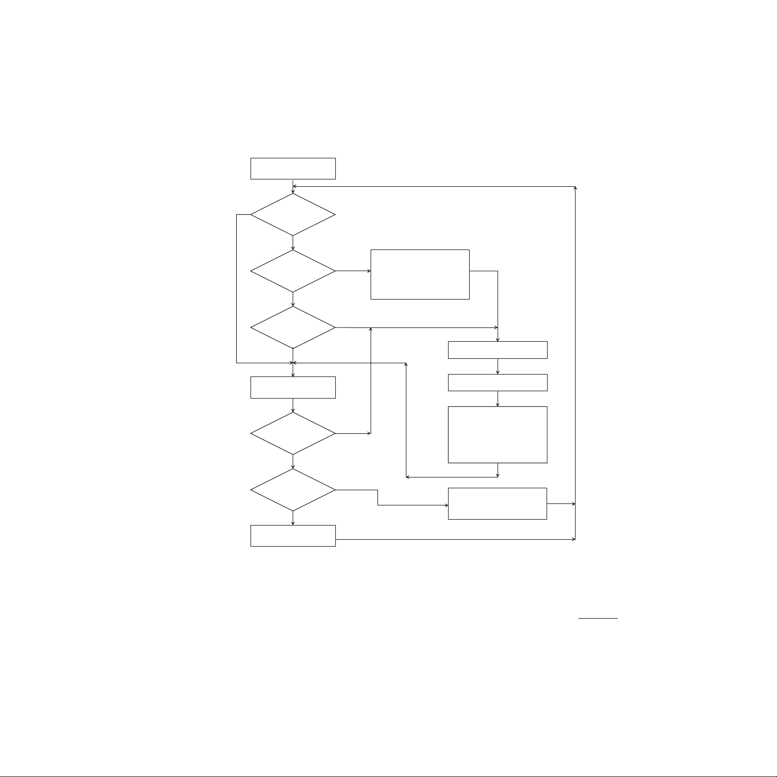
executed when the interrupt took place. Figure 4-1 shows the sequence of events
that occur during interrupt processing.
From
RESET
Y
Is
I-Bit
Set?
N
IRQ
External
Interrupt?
N
TIMER
Internal
Interrupt?
N
Fetch Next
Instruction
SWI
Instruction
?
N
RTI
Instruction
?
N
Execute
Instruction
Y
Y
Y
Y
Clear IRQ
Request
Latch if IRQE1 is
cleared
Stack PC, X, A, CC
Set I-Bit in CCR
Load PC From:
SWI: $0FFC, $0FFD
IRQ: $0FFA-$0FFB
TIMER: $0FF8-$0FF9
TIMER1: $0FF6-$0FF7
Restore Registers
from stack
CC, A, X, PC
Figure 4-1. Interrupt Processing Flowchart
4.2 RESET INTERRUPT SEQUENCE
The RESET function is not in the strictest sense an interrupt; however, it is acted
upon in a similar manner as shown in Figure 4-1. A low level input on the RESET
pin or an internally generated RST signal causes the program to vector to its starting address which is specified by the contents of memory locations $0FFE and
$0FFF. The I-bit in the condition code register is also set.
MOTOROLA INTERRUPTS MC68HC05J5A
4-2 REV 2.1
Page 29
July 16, 1999 GENERAL RELEASE SPECIFICATION
4.3 SOFTWARE INTERRUPT (SWI)
The SWI is an executable instruction and a non-maskable interrupt since it is executed regardless of the state of the I-bit in the CCR. As with any instruction, interrupts pending during the previous instruction will be serviced before the SWI
opcode is fetched. The interrupt service routine address is specified by the contents of memory locations $0FFC and $0FFD.
4.4 HARDWARE INTERRUPTS
All hardware interrupts except RESET are maskable by the I-bit in the CCR. If the
I-bit is set, all hardware interrupts (internal and external) are disabled. Clearing
the I-bit enables the hardware interrupts. There are two types of hardware interrupts which are explained in the following sections.
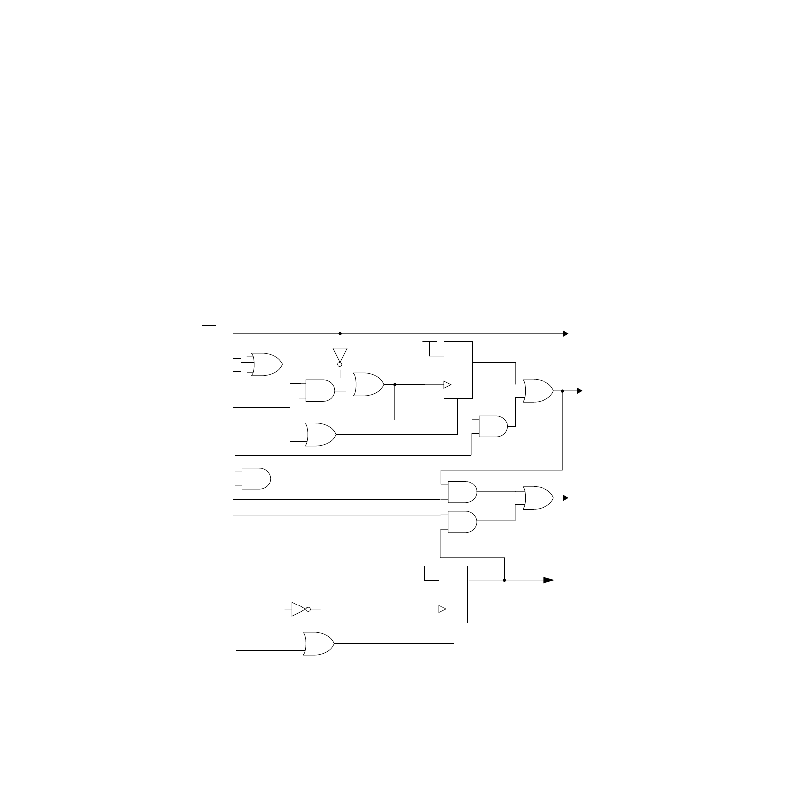
4.5 EXTERNAL INTERRUPT (IRQ
The IRQ
pin provides an asynchronous interrupt to the CPU. A block diagram of
the IRQ function is shown in Figure 4-2.
IRQ Pin
PA0
PA1
PA2
PA3
Mask Option
(Port A External Int.)
RST
IRQR
Mask Option
(IRQ Level)
IRQ Fetch Vector
IRQE1
IRQE
IRQE1
)
V
DD
IRQ
LATCH
R
to BIH & BIL
instruction
sensing
IRQF
to IRQ
processing
in CPU
V
DD
IRQ1
LATCH
PA7
R
RST
IRQR1
IRQF1
Figure 4-2. IRQ Function Block Diagram
MC68HC05J5A INTERRUPTS MOTOROLA
REV 2.1 4-3
Page 30

GENERAL RELEASE SPECIFICATION July 16, 1999
The IRQ pin is a source of IRQ interrupts and a mask option can also enable the
other four lower Port A pins (PA0 thru PA3) to act as other IRQ interrupt sources.
The last source of IRQ interrupt comes from PA7 whenever there is a falling edge
on PA7 and IRQE1 is enabled. There is no mask option associated with PA7 interrupt.
Refer to Figure 4-2 for the following descriptions. IRQ interrupt source comes
from IRQ and IRQ1 latches. The IRQ latch will be set on the falling edge of the
pin or on any rising edge of PA0-3 pins if PA0-3 interrupts have been enabled.
IRQ
The IRQ1 latch will be set on the falling edge of PA7 if PA7 interrupt has been
enabled. If "edge-only" sensitivity is chosen by a mask option, only the IRQ latch
output can activate an IRQF flag which creates a request to the CPU to generate
the IRQ interrupt sequence. This makes the IRQ interrupt sensitive to the f ollowing
cases:
1. Falling edge on the IRQ
pin.
2. Rising edge on any PA0-PA3 pin with IRQ enabled (via mask option).
If level sensitivity is chosen, the rising edge signal on the clock input of the IRQ
latch can also activate an IRQF flag which creates an IRQ request to the CPU to
generate the IRQ interrupt sequence. This makes the IRQ interrupt sensitive to
the following cases:
1. Low level on the IRQ
2. Falling edge on the IRQ
pin.
pin.
3. High level on any PA0- PA3 pin with IRQ enabled (via mask option).
4. Rising edge on any PA0- PA3 pin with IRQ enabled (via mask option).
The IRQE enable bit controls whether an active IRQF flag can generate an IRQ
interrupt sequence. This interrupt is serviced by the interrupt service routine
located at the address specified by the contents of $0FFA and $0FFB.
The IRQ latch is automatically cleared by entering the interrupt service routine IF
IRQE1 enable bit is cleared. If IRQE1 enable bit is also set, the only way of clearing IRQF is by writing a logic one to the IRQR acknowledge bit. Writing a logic one
to the IRQR acknowledge bit in the ICSR is the other way of clearing IRQF flag,
regardless of the status of the IRQE1 bit, besides IRQ vector fetch. This conditional reset of IRQF flag provides a way for the user to differentiate the interrupt
sources from IRQ and IRQ1 latches and also to make it J1A compatible if PA7
interrupt is not used. As long as the output state of the IRQF flag bit is active the
CPU will continuously re-enter the IRQ interrupt sequence until the active state is
removed or the IRQE enable bit is cleared.
PA7 interrupt source, if enabled by IRQE1 enable bit, triggers IRQ interrupt on
PA7 f alling edge only. The IRQ1 latch (IRQF1 flag) can ONLY be cleared by writing
a logic one to the IRQR1 acknowledge bit in the ICSR. IRQ vector fetch can NOT
clear IRQF1 flag. IRQ interrupt caused by PA7 falling edge also vectors to $0FFA
and $0FFB.
MOTOROLA INTERRUPTS MC68HC05J5A
4-4 REV 2.1
Page 31

July 16, 1999 GENERAL RELEASE SPECIFICATION
4.5.1 IRQ CONTROL/STATUS REGISTER (ICSR) $0A
The IRQ interrupt function is controlled by the ICSR located at $000A. All unused
bits in the ICSR will read as logic zeros. The IRQF, IRQF1, IRQE1 bits are cleared
and IRQE bit is set by reset.
ICSR
$000A
7
R
IRQE
W
reset⇒
1
RESERVED FOR TEST
6543210
0
IRQE1
0000000
R
0 IRQF1
R
IRQF 0
IRQR
UNIMPLEMENTED
Figure 4-3. IRQ Status & Control Register
IRQR 1 - PA7 Interrupt Acknowledge
The IRQR1 acknowledge bit clears an IRQ interrupt triggered by a falling edge
on PA7 by clearing the IRQ1 latch. The IRQR1 ackno wledge bit will alw a ys read
as a logic zero.
1 = Writing a logic one to the IRQR1 acknowledge bit will clear the IRQ1
latch.
0 = Writing a logic zero to the IRQR1 acknowledge bit will have no effect
on the IRQ1 latch.
IRQR - IRQ Interrupt Acknowledge
The IRQR acknowledge bit clears an IRQ interrupt by clearing the IRQ latch.
The IRQR acknowledge bit will always read as a logic zero.
1 = Writing a logic one to the IRQR acknowledge bit will clear the IRQ
latch.
0 = Writing a logic zero to the IRQR acknowledge bit will have no effect
on the IRQ latch.
0
IRQR1
IRQF1 - PA7 Interrupt Request Flag
Writing to the IRQF1 flag bit will have no effect on it. If the additional setting of
IRQF1 flag bit is not cleared in the IRQ service routine and the IRQE1 enable
bit remains set the CPU will re-enter the IRQ interrupt sequence continuously
until either the IRQF1 flag bit or the IRQE1 enable bit is cleared. The IRQF1
latch is cleared by reset.
1 = Indicates that an IRQ request triggered by a falling edge on PA7 is
pending.
0 = Indicates that no IRQ request triggered by a falling edge on PA7 is
pending. The IRQF1 flag bit can ONLY be cleared by writing a logic
one to the IRQR1 acknowledge bit. Doing so before exiting the
service routine will mask out additional occurrences of the IRQF1.
MC68HC05J5A INTERRUPTS MOTOROLA
REV 2.1 4-5
Page 32

GENERAL RELEASE SPECIFICATION July 16, 1999
IRQF - IRQ Interrupt Request Flag
Writing to the IRQF flag bit will have no eff ect on it. If the additional setting of IRQF
flag bit is not cleared in the IRQ service routine and the IRQE enable bit remains
set the CPU will re-enter the IRQ interrupt sequence continuously until either the
IRQF flag bit or the IRQE enable bit is clear. The IRQF latch is cleared by reset.
1 = Indicates that an IRQ request is pending.
0 = Indicates that no IRQ request triggered by pins PA0-3 or IRQ
pending. The IRQF flag bit is cleared once the IRQ vector is fetched
AND if IRQE1 is also cleared. If IRQE1 is set, then the only way of
clearing IRQF flag is by writing a logic one to IRQR bit. The IRQF
flag bit can be cleared, regardless of the status of the IRQE1 bit, by
writing a logic one to the IRQR acknowledge bit to clear the IRQ
latch and also conditioning the external IRQ sources to be inactive
(if the level sensitive interrupts are enabled via mask option). Doing
so before exiting the service routine will mask out additional
occurrences of the IRQF.
IRQE1 - PA7 Interrupt Enable
The IRQE1 bit enables/disables the IRQF1 flag bit to initiate an IRQ interrupt
sequence.
1 = Enables IRQF1 interrupt, that is, the IRQF1 flag bit can generate an
interrupt sequence. Execution of the STOP or WAIT instructions will
leave the IRQE1 bit to be UNAFFECTED.
0 = The IRQF1 flag bit cannot generate an interrupt sequence. Reset
clears the IRQE1 enable bit, thereby disabling PA7 interrupts.
is
IRQE - IRQ Interrupt Enable
The IRQE bit enables/disables the IRQF flag bit to initiate an IRQ interrupt
sequence.
1 = Enables IRQF interrupt, that is, the IRQF flag bit can generate an
interrupt sequence. Reset sets the IRQE enable bit, thereby
enabling IRQ interrupts once the I-bit is cleared. Execution of the
STOP or WAIT instructions causes the IRQE bit to be set in order to
allow the external IRQ to exit these modes.
0 = The IRQF flag bit cannot generate an interrupt sequence.
4.5.2 OPTIONAL EXTERNAL INTERRUPTS (PA0-PA3)
The IRQ interrupt can also be triggered by the inputs on the PA0 thru PA3 port
pins if enabled by a single mask option. If enabled, the lower four bits of Port A
can activate the IRQ interrupt function, and the interrupt operation will be the
same as for inputs to the IRQ
pin. This mask option of PA0-3 interr upt allow all of
these input pins to be OR’ed with the input present on the IRQ
PA3 pins must be selected as a group as an additional IRQ interrupt. All the PA0-3
interrupt sources are also controlled by the IRQE enable bit.
pin. All PA0 thru
MOTOROLA INTERRUPTS MC68HC05J5A
4-6 REV 2.1
Page 33

July 16, 1999 GENERAL RELEASE SPECIFICATION
NOTE
The BIH and BIL instructions will only apply to the level on the IRQ pin itself, and
not to the output of the logic OR function with the PA0 thru PA3 pins. The state of
the individual Port A pins can be checked by reading the appropriate Port A pins
as inputs.
NOTE
If enabled, the PA0 thr u PA3 and PA7 pins will cause an IRQ interrupt regardless
of whether these pins are configured as inputs or outputs.
4.5.3 TIMER INTERRUPT (MFT)
The TIMER interrupt is generated by the multi-function timer when either a timer
overflow or a real time interrupt has occurred as described in Section 8. The interrupt flags and enable bits for the Timer interrupts are located in the Timer Control
& Status Register (TCSR) located at $0008. The I-bit in the CCR must be clear in
order for the TIMER interrupt to be enabled. Either of these two interrupts will vector to the same interrupt service routine located at the address specified by the
contents of memory locations $0FF8 and $0FF9.
4.5.4 TIMER1 INTERRUPT (16-BIT TIMER)
The Timer1 interrupt is generated by the 16-bit Timer when either a timer1 overflow or a input capture has occurred as described in Section 9. The interrupt flags
and enable bits for the Timer1 interrupt are located in the Timer1 Control & Status
Register (T1CR & T1SR) located at $0012, $0013. The I-bit in the CCR must be
cleared in order to enable the Timer1. Either of these two interrupts will vector to
the same interrupt service routine located at the address specified by the contents
of memory locations $0FF6 and $0FF7.
MC68HC05J5A INTERRUPTS MOTOROLA
REV 2.1 4-7
Page 34

GENERAL RELEASE SPECIFICATION July 16, 1999
MOTOROLA INTERRUPTS MC68HC05J5A
4-8 REV 2.1
Page 35

July 16, 1999 GENERAL RELEASE SPECIFICATION
SECTION 5
RESETS
The MCU can be reset from five sources: one external input and four internal
restart conditions.
• Initial power up of device (power on reset)
• A logic zero applied to the RESET
pin (external reset)
• Timeout of the COP watchdog (COP reset)
• Low voltage applied to the device (LVR reset)
• Fetch of an opcode from an address not in the memory map (illegal
address reset)
Figure 5-1 shows a block diagram of the reset sources and their interaction.
IRQ
V
DD
R
LATCH
RESET
OSC
Data
Address
Address
V
DD
COP Watchdog
(COPR)
Illegal Address
(ILADR)
Power-On Reset
(POR)
PH2
R
S
LATCH
CPU
RST
To Interrupt
logic
Mode
Select
To other
peripherals
Low Voltage Reset
(LVR)
Figure 5-1. Reset Block Diagram
MC68HC05J5A RESETS MOTOROLA
REV 2.1 5-1
Page 36

GENERAL RELEASE SPECIFICATION July 16, 1999
5.1 EXTERNAL RESET (RESET)
The RESET
pin is the only external source of a reset. This pin is connected to a
Schmitt trigger input gate to provide an upper and lower threshold voltage separated by a minimum amount of hysteresis. This external reset occurs whenever
the RESET
RESET
pin is pulled below the lower threshold and remains in reset until the
pin rises above the upper threshold. This active low input will generate the
RST signal and reset the CPU and peripherals. This pin is also an output pin
whenever the LVR triggers an inter nal reset. Termination of the external RESET
input or the internal COP Watchdog reset or LVR are the only reset sources that
can alter the operating mode of the MCU.
Activation of the RST signal is generally referred to as reset of the device, unless
otherwise specified.
5.2 INTERNAL RESETS
The four internally generated resets are the initial power-on reset function, the
COP Watchdog Timer reset, the illegal address detector reset and the low voltage
reset (LVR). Termination of the external RESET input or the inter nal COP Watchdog Timer or LVR are the only reset sources that can alter the operating mode of
the MCU. The other internal resets will not have any effect on the mode of operation when their reset state ends.
NOTE
5.2.1 POWER-ON RESET (POR)
The internal POR is generated on power-up to allow the clock oscillator to stabilize. The POR is strictly for power turn-on conditions and is not able to detect a
drop in the power supply voltage (brown-out). There is an oscillator stabilizing
delay after the oscillator becomes active. The delay time could be 224 or 4064 of
internal processor bus clock cycles (PH2) which is a mask option.
The POR will generate the RST signal which will reset the CPU. If any other reset
function is active at the end of this delay time, the RST signal will remain in the
reset condition until the other reset condition(s) end.
5.2.2 COMPUTER OPERATING PROPERLY RESET (COPR)
The internal COPR reset is generated automatically (if the COP is enabled) by a
time-out of the COP Watchdog Timer. This time-out occurs if the counter in the
COP Watchdog Timer is not reset (cleared) within a specific time by a software
reset sequence. The COP Watchdog Timer can be disabled by a mask option.
Refer to Section 8.2 for more information on this time-out feature. COP reset also
forces the RESET
pin low
MOTOROLA RESETS MC68HC05J5A
5-2 REV 2.1
Page 37

July 16, 1999 GENERAL RELEASE SPECIFICATION
The COPR will generate the RST signal which will reset the CPU and other
peripherals. Also, the COPR will establish the mode of operation based on the
state of the IRQ
pin is at the V
RESET
pin will determine which Test Mode (Inter nal or Expanded) the MCU will
be in. If the voltage at the IRQ
pin at the time the COPR signal ends. If the voltage on the IRQ
level, the state of the PB0 pin during the last rising edge of the
TST
pin is in the normal operating range (VSS to VDD),
the MCU will enter Single-Chip Mode when the COPR signal ends. If any other
reset function is active at the end of the COPR reset signal, the RST signal will
remain in the reset condition until the other reset condition(s) end.
5.2.3 LOW VOLTAGE RESET (LVR)
The internal LVR reset is generated when V
ger value V
for at least one t
LVR
. In typical applications, the power supply de-
CYC
coupling circuit will eliminate negative-going voltage glitches of less than one
. This reset will hold the MCU in the reset state until VDD rises above V
t
CYC
Whenever V
is above V
DD
and below 4.5V, the MCU is guaranteed to operate
LVR
although not within specification. The output from the LVR is connected directly to
the internal reset circuitry and also forces the RESET
will be removed once the power supply voltage rises above V
normal power-on-reset sequence occurs.
5.2.4 ILLEGAL ADDRESS RESET (ILADR)
The internal ILADR reset is generated when an instruction opcode fetch occurs
from an address which is not implemented in the RAM ($0080 - $00FF) nor ROM
($0300-$0CFF, $0E00-$0FFF). The ILADR will generate the RST signal which will
reset the CPU and other peripherals. If an y other reset function is activ e at the end
of the ILADR reset signal, the RST signal will remain in the reset condition until
the other reset condition(s) end. Notice that ILADR also f orces the RESET
falls below the specified LVR trig-
DD
pin low. The internal reset
, at which time a
LVR
pin low .
LVR
.
MC68HC05J5A RESETS MOTOROLA
REV 2.1 5-3
Page 38

GENERAL RELEASE SPECIFICATION July 16, 1999
MOTOROLA RESETS MC68HC05J5A
5-4 REV 2.1
Page 39

July 16, 1999 GENERAL RELEASE SPECIFICATION
SECTION 6
LOW POWER MODES
There are three modes of operation that reduce power consumption:
• Stop mode
• Wait mode
• Halt mode
The WAIT and STOP instructions provide two power saving modes by stopping
various internal modules and/or the on-chip oscillator. The STOP and WAIT
instructions are not normally used if the COP Watchdog Timer is enabled. A mask
option is provided to convert the STOP instruction to a HALT, which is a WAIT-like
instruction that does not halt the COP Watchdog Timer but has a recovery delay.
The flow of the STOP, HALT, and WAIT modes are shown in Figure 6-1.
MC68HC05J5A LOW POWER MODES MOTOROLA
REV 2.1 6-1
Page 40

GENERAL RELEASE SPECIFICATION July 16, 1999
STOP HALT
Stop
Conversion to
Halt?
N
Stop External Oscillator,
Stop Internal Timer Clock,
Reset Startup Delay
Stop Internal Processor Clock,
Clear I-Bit in CCR,
and set IRQE in ICSR
External
RESET?
N
IRQ
External
Interrupt?
N
Y
Y
Y
Restart External Oscillator,
start Stabilization Delay
End
of Stabilization
Delay?
N
Internal Processor Clock
External Oscillator Active
Internal Timer Clock Active
Stop Internal Processor Clock,
Clear I-Bit in CCR,
and set IRQE in ICSR
Y
Y
Y
Y
Y
Restart
External
RESET?
External
Interrupt?
TIMER
Internal
Interrupt?
Internal
RESET?
and
IRQ
COP
WAIT
External Oscillator Active
and
Internal Timer Clock Active
Stop Internal Processor Clock,
Clear I-Bit in CCR,
and set IRQE in ICSR
N
Y
N
Y
N
Y
N
Y
External
RESET?
N
IRQ
External
Interrupt?
N
TIMER
Internal
Interrupt?
N
COP
Internal
RESET?
N
1. Fetch Reset Vector
or
2. Service Interrupt
a. Stack
b. Set I-Bit
c. Vector to Interrupt Routine
Figure 6-1. STOP/HALT/WAIT Flowcharts
6.1 STOP INSTRUCTION
The STOP instruction can result in one of two modes of operation depending on
the STOP mask option chosen. One option is for the STOP instruction to operate
like the STOP in normal MC68HC05 family members and place the device in the
MOTOROLA LOW POWER MODES MC68HC05J5A
6-2 REV 2.1
Page 41

July 16, 1999 GENERAL RELEASE SPECIFICATION
STOP Mode. The other option is for the STOP instruction to behave like a WAIT
instruction (except that the restart time will involve a dela y) and place the device in
the HALT Mode.
6.1.1 STOP Mode
Execution of the ST OP instruction in this mode (selected by a mask option) places
the MCU in its lowest power consumption mode. In the STOP Mode the internal
oscillator is turned off, halting all internal processing, including the COP W atchdog
Timer.
When the CPU enters STOP Mode the interrupt flags (TOF and RTIF) and the
interrupt enable bits (TOFE and RTIE) in the TCSR are cleared by internal hardware to remove any pending timer interrupt requests and to disable any further
timer interrupts. Execution of the STOP instruction automatically clears the I-bit in
the Condition Code Register and sets the IRQE enable bit in the IRQ Control/Status Register so that the IRQ external interrupt is enabled. All other registers,
including the other bits in the TCSR, and memory remain unaltered. All input/output lines remain unchanged.
The MCU can be brought out of the STOP Mode only b y an IRQ external interrupt
or an externally generated RESET or an LVR reset. When exiting the STOP Mode
the internal oscillator will resume after a 224 or 4064 internal processor clock
cycle oscillator stabilizing delay which is selected by a mask option.
Execution of the STOP instruction with the STOP Mode Mask Option will cause
the oscillator to stop and therefore disable the COP Watchdog Timer. If the COP
Watchdog Timer is to be used, the STOP Mode should be changed to the HALT
Mode by choosing the appropriate mask option. See Section 6.4 for more details.
6.1.2 HALT Mode
Execution of the ST OP instruction in this mode (selected by a mask option) places
the MCU in a low-power mode, which consumes more power than the STOP
Mode. In the HALT Mode the internal processor clock is halted, suspending all
processor and internal bus activity. Internal timer clocks remain active, permitting
interrupts to be generated from the timer (MFT or Timer 1) or a reset to be generated from the COP Watchdog Timer. Execution of the STOP instruction automatically clears the I-bit in the Condition Code Register and sets the IRQE enable bit
in the IRQ Control/Status Register so that the IRQ external interrupt is enabled.
All other registers, memory, and input/output lines remain in their previous states.
NOTE
The HALT Mode may be terminated by a Timer interrupt, an external IRQ, an LVR
reset, or external RESET
occurs. Since the internal timer is still running in the
HALT mode, the wake up delay timer (oscillator stabilizing delay timer) may star t
counting from an unknown value. So, the internal processor clock will resume
MC68HC05J5A LOW POWER MODES MOTOROLA
REV 2.1 6-3
Page 42

GENERAL RELEASE SPECIFICATION July 16, 1999
after a varied delay time which is from one to 224 or 4064 internal processor clock
cycles (the POR delay time). The HALT Mode is not intended for normal use, but
is provided to keep the COP Watchdog Timer active should the STOP instruction
opcode be inadvertently executed.
6.2 WAIT INSTRUCTION
The WAIT instruction places the MCU in a low-power mode, which consumes
more power than the STOP Mode. In the WAIT Mode the internal processor clock
is halted, suspending all processor and internal bus activity. Internal timer clocks
remain active, permitting interrupts to be generated from the timer or a reset to be
generated from the COP Watchdog Timer. Execution of the WAIT instruction automatically clears the I-bit in the Condition Code Register and sets the IRQE enable
bit in the IRQ Control/Status Register so that the IRQ external interrupt is enabled.
All other registers, memory, and input/output lines remain in their previous states.
If timer (MFT or Timer 1) interrupts are enabled, a TIMER interrupt will cause the
processor to exit the WAIT Mode and resume normal operation. The Timer ma y be
used to generate a periodic exit from the WAIT Mode. The WAIT Mode may also
be exited when an external IRQ or an LVR reset or an external RESET occurs.
6.3 DATA-RETENTION MODE
If the LVR mask option is selected and since LVR kicks in whenever V
the specified LVR trigger voltage which is higher than that required of the Data
Retention mode, the Data Retention mode will not exist. Data Retention Mode is
only meaningful if LVR mask option is not selected.
The contents of RAM and CPU registers are retained at supply voltage as low as
2.0 VDC. This is called the data-retention mode where the data is held, but the
device is not guaranteed to operate. The RESET
data-retention mode.
6.4 COP W A TCHDOG TIMER CONSIDERA TIONS
The COP Watchdog Timer is active in all modes of operation if enabled by a mask
option. Thus, emulation of applications that do not service the COP should only be
done with devices that have the COP Mask Option disabled.
If the COP Watchdog Timer is selected by the mask option, any execution of the
STOP instruction (either intentional or inadvertent due to the CPU being disturbed) will cause the oscillator to halt and prevent the COP Watchdog Timer from
timing out unless the STOP to HALT conversion feature is enabled. Therefore, it is
recommended that the STOP instruction should be conver ted to a HALT instruction if the COP Watchdog Timer is enabled.
is below
DD
pin must be held low during
If the COP Watchdog Timer is selected by the mask option, the COP will reset the
MCU when it times out. Therefore, it is recommended that the COP Watchdog
should be disabled for a system that m ust ha v e intentional uses of the WAIT Mode
for periods longer than the COP time-out period.
MOTOROLA LOW POWER MODES MC68HC05J5A
6-4 REV 2.1
Page 43

July 16, 1999 GENERAL RELEASE SPECIFICATION
The recommended interactions and considerations for the COP Watchdog Timer,
STOP instruction, and WAIT instruction are summarized in Table 6-1.
Table 6-1. COP Watchdog Timer Recommendations
IF the following conditions exist:
STOP Instruction WAIT Time
converted to HALT
by mask option
converted to HALT
by mask option
Acts as STOP
WAIT Time less than
COP Time-Out
WAIT Time more than
COP Time-Out
any length
WAIT Time
THEN the
COP Watchdog Timer
should be as follows:
Enable or disable COP
by mask option
Disable COP
by mask option
Disable COP
by mask option
MC68HC05J5A LOW POWER MODES MOTOROLA
REV 2.1 6-5
Page 44

GENERAL RELEASE SPECIFICATION July 16, 1999
MOTOROLA LOW POWER MODES MC68HC05J5A
6-6 REV 2.1
Page 45

July 16, 1999 GENERAL RELEASE SPECIFICATION
SECTION 7
INPUT/OUTPUT PORTS
In the normal operating mode there are 14 usable bidirectional I/O lines arranged
as one 8-bit I/O port (Port A), and one 6-bit I/O port (Port B). The individual bits in
these ports are programmable as either inputs or outputs under software control
by the data direction registers (DDR’s). Also, if enabled by a single mask option all
Port A and Por t B I/O pins may have individual software programmable pull-down
or pull-up devices. Also, PA4-PA7 and PB1-PB2 pins have high current sink capability; PA0-PA3 may function as additional IRQ
both PA6 and PA7 pins have Schmitt trigger input for better noise immunity. V
and VIL specified at 2.4V and 0.8V, respectively.
The four port pins, PB2-PB5 are only availab le on the 20-pin version of the device.
interrupt input sources. Note that
IH
7.1 SLOW OUTPUT FALLING-EDGE TRANSITION
DDRB
$0005
7
R
SLOWE
W
0
6543210
0
DDRB3DDRB4DDRB5
0000000reset⇒
Figure 7-1. Port B Data Direction Register
SLOWE - Slow Transition Enable
The slow transition feature is controlled by the SLOWE bit of DDRB (Port B
Data Direction Register).
1 = Enables the slow falling-edge output transition feature on the four I/
O lines: PA6, PA7, PB1, and PB2. If the pin is configured as an
output pin.
0 = Disables slow falling-edge output transition feature on the four I/O
lines: PA6, PA7, PB1, and PB2. Default value of SLOWE bit is
cleared.
DDRB1DDRB2
DDRB0
7.2 PORT A
Port A is a 8-bit bidirectional port which shares five of its pins with the IRQ interrupt system as shown in Figure 7-2. Note that both PA6 and PA7 pins have
Schmitt trigger input for better noise immunity. Only the PA6 and PA7 pins are
open-drained type with slow output transition feature.
MC68HC05J5A INPUT/OUTPUT PORTS MOTOROLA
REV 2.1 7-1
Page 46

GENERAL RELEASE SPECIFICATION July 16, 1999
Each Port A pin is controlled by the corresponding bits in a data direction register,
a data register and a pulldown/up register. The Port A Data Register is located at
address $0000. The Por t A Data Direction Register (DDRA) is located at address
$0004. The Por t A Pulldown/up Register (PDURA) is located at address $0010.
Reset operation will clear the DDRA and the PDURA. The Port A Data Register is
unaffected by reset.
Read $0004
Write $0004
Write $0000
Read $0000
Write $0010
Internal HC05
Data Bus
Note1: All the I/O port pins may have either pullup or pulldown device.
Note2: PA6 and PA7 output drivers are the open-drained type
Reset
(RST)
Data Direction
Register Bit
Data
Register Bit
Pulldown/up
Register Bit
(Software Pulldown/up Inhibit)
Figure 7-2. Port A I/O Circuitry
Mask Option
VDD
5K
Pullup
Output
8 mA Sink
Capability
(Bits 4-7 Only)
100 µA
Pulldown
PA0-PA3 and PA7 only:
to IRQ
interrupt system
I/O
Pin
7.2.1 Port A Data Register
Each Port A I/O pin has a corresponding bit in the Por t A Data Register. When a
Port A pin is programmed as output, the corresponding data register bit determines the logic state of that pin. When a Por t A pin is programmed as input, any
read from the Port A Data Register will return the logic state of the corresponding
I/O pin. The Port A data register is unaffected by reset.
7.2.2 Port A Data Direction Register
Each Port A I/O pin may be programmed as input by clearing the corresponding
bit in the DDRA, or programmed as output by setting the corresponding bit in the
DDRA. The DDRA can be accessed at address $0004. The DDRA is cleared by
reset.
If configured as output pins, PA6 and PA7 have slow output falling-edge transition
feature. The slow transition feature is controlled by the SLOWE bit of DDRB.
SLOWE bit, if set and if the pin is configured as an output pin, enables the slow
falling-edge output transition feature of all four I/O lines, PA6, PA7, PB1, and PB2.
MOTOROLA INPUT/OUTPUT PORTS MC68HC05J5A
7-2 REV 2.1
Page 47

July 16, 1999 GENERAL RELEASE SPECIFICATION
7.2.3 Port A Pulldown/up Register
All Port A I/O pins may ha v e softw are prog rammab le pulldo wn/up devices enabled
by the applicable mask option. If the pulldown/up mask option is selected, the pulldown/up is activated whenever the corresponding bit in the PDURA is clear. If the
corresponding bit in the PDURA bit is set or the mask option for pulldown/up is not
chosen, the pulldown/up will be disabled. A pulldown on an I/O pin is activated
only if the I/O pin is programmed as an input whereas a pullup device on an I/O
pin is always activated whenever enabled, regardless of port direction.
The PDURA is a write-only register. Any reads of location $0010 will return undefined results. Since reset clears both the DDRA and the PDURA, all pins will initialize as inputs with the pulldown active and pullup devices active (if enabled by
mask option).
Typical value of port A pullup is 5KΩ.
7.2.4 Port A Drive Capability
The outputs for the upper four bits of Port A (PA4, PA5, PA6 and PA7) are capable
of sinking approximately 8mA of current to V
SS
.
7.2.5 Port A I/O Pin Interrupts
The inputs to PA0, PA1, PA2, PA3 may be connected to the IRQ input of the CPU
if enabled by a mask option. The input to PA7 is also connected to the IRQ input of
the CPU, yet it is only enabled or disabled by software, not by mask option. PA7
interrupt capability is controlled by a set of control and status bits (IRQE1, IRQF1,
IRQR1), different from the set of control and status bits for that of PA0-PA3 and
pin (IRQE, IRQF, IRQR) in the same ICSR (Interrupt Control and Status Reg-
IRQ
ister).
When connected as an alternate source of an IRQ interrupt, PA0-3 input pins will
behave the same as the IRQ
or a rising edge. The IRQ
edge. PA7 interrupt occurs, if enabled, only upon the falling edge at the input.
If mask options for both level and edge sensitivity interrupts are chosen, the presence of a logic one or occurrence of a rising edge on any one of the lower four
Port A pins will cause an IRQ interrupt request. If the edge-only sensitivity is
selected, the occurrence of a rising edge on any one of the lower four Port A pins
will cause an IRQ interrupt request. As long as any one of the lower four Port A
IRQ inputs remains at a logic one level, the other of the lower four Port A IRQ
inputs are effectively ignored.
pin itself, e xcept that their activ e state is a logical one
pin has an active state that is a logical zero or a falling
NOTE
The BIH and BIL instructions will only apply to the level on the IRQ pin itself, and
not to the internal IRQ input to the CPU. Therefore BIH and BIL cannot be used to
test the state of the lower four Port A input pins as a group nor that of PA7.
MC68HC05J5A INPUT/OUTPUT PORTS MOTOROLA
REV 2.1 7-3
Page 48

GENERAL RELEASE SPECIFICATION July 16, 1999
7.3 PORT B
Port B is a 6-bit bidirectional port which functions as shown in Figure 7-3. Only
PB1 and PB2 are of open-drained type. Each Port B pin is controlled by the corresponding bits in a data direction register, a data register and a pulldown/up register. The Port B Data Register is located at address $0001. The Port B Data
Direction Register (DDRB) is located at address $0005. The Por t B Pulldown/up
Register (PDURB) is located at address $0011. Reset clears the DDRB and the
PDURB. The Port B Data Register is unaffected by reset.
Please note that only PB0 and PB1 pins are bonded out in the 16-pin package
type. Actually, the PB1 and PB2 I/O port lines are short and bonded to the PB1 on
the 16-pin package. Both PB1 and PB2 are of open-drained type, capable of typically sinking 25 mA current at V
0.5V max. In order to constitute a single pin
OL
capable of typically sinking 50 mA, both PB1 and PB2 have to be written with the
same value at the same write cycle.
Read $0005
Write $0005
Write $0001
Data Direction
Register Bit
Data
Register Bit
Read $0001
Write $0011
Internal HC05
Data Bus
Note1: All the I/O port pins may have either pullup or pulldown device.
Note2: PB1 and PB2 output drivers are the open-drained type
Reset
(RST)
Port Pin PB0 is shared with TCAP input of the 16-Timer input capture function.
The input capture function can be programmed for a positive edge or the negative
edge TCAP input. When an expected edge is generated on this pin, the counter
value at that moment will be captured into a capture register. For the details about
this feature please refer to the Section 9.
Pulldown/up
Register Bit
(Software Pulldown/up Inhibit)
Figure 7-3. Port B I/O Circuitry
Mask Option
Output
VDD
30K
Pullup
I/O
Pin
100 µA
Pulldown
7.3.1 Port B Data Register
All Port B I/O pins have a corresponding bit in the Port B Data Register. When a
Port B pin is programmed as output the corresponding data register bit
determines the logic state of the output pin. When a Port B pin is programmed as
input, any read from the Port B Data Register will return the logic state of the
MOTOROLA INPUT/OUTPUT PORTS MC68HC05J5A
7-4 REV 2.1
Page 49

July 16, 1999 GENERAL RELEASE SPECIFICATION
corresponding I/O pin. The P ort B data register is unaffected by reset. Unused bits
6 and 7 will always read as logic zeros, and any write to these bits will be ignored.
The Port B data register is unaffected by reset.
7.3.2 Port B Data Direction Register
Port B I/O pins may be programmed as an input by clearing the corresponding bit
in the DDRB, or programmed as an output by setting the corresponding bit in the
DDRB. The DDRB can be accessed at address $0005. Unused bits 6 and 7 will
always read as logic zeros, and any write to these bits will be ignored.The DDRB
is cleared by reset.
If configured as output pins, PB1 and PB2 have slow output falling-edge transition
feature. The slow transition feature is controlled by the SLOWE bit of DDRB.
SLOWE bit, if set and if the pin is configured as an output pin, enables the slow
falling-edge output transition feature of all four I/O lines, PA6, PA7, PB1 and PB2.
For the 16-pin package type, care should be taken in using PB1 pin, which is
bonded to two internal port B I/O lines PB1 and PB2, to constitute a 50mA current
sinking driver. Both PB1 and PB2 I/O lines are capable of sinking 25mA. If they
are written with the same logic 0 value in the same write cycle, PB1 pin will sink
50 mA. If the y are written with diff erent values in the same write cycle, PB1 pin will
sink only 25mA.
For the 20-pin package type, I/O lines PB1 and PB2 are not bonded to the same
pin. Hence , to constitute a 50mA current sinking driver, PB1 and PB2 pins have to
be tied together externally and controlled in the same way as in the16-pin package type case.
Also, if the slow transition feature of pin PB1 is enabled, a combination of I/O lines
PB1 and PB2, is also a combination of slow transition features of I/O lines PB1
and PB2. PB2 line falling-edge output transition occurs t
cycle, with a standard I/O edge transition time. Whereas for PB1 line, the fallingedge transition occurring immediately after the write cycle, but with an edge transition time slower than standard I/Os, similar to PA6 and PA7 pins.
The net result is, for the 16-pin package type, since both PB1 and PB2 I/O lines
are bonded to the same PB1 pin, the combination of delayed PB1 line sharp-edge
output and the non-delayed slow transition output yields the desired slow output
falling-edge transition.
For the 20-pin package, PB1 and PB2 pins should be tied externally to create a
driver with the desired slow output falling-edge transition feature. If SLOWE is set
and PB2 pin is not tied to PB1 pin, be advised that the output at PB2 changes
state t
/2 after the write cycle.
CYC
7.3.3 Port B Pulldown/up Register
/2 after the write
CYC
All Port B I/O pins may ha v e softw are prog rammab le pulldo wn/up devices enabled
by a mask option. If the pulldown/up mask option is selected, the pulldown/up is
activated whenever the corresponding bit in the PDURB is clear. A pulldown on an
MC68HC05J5A INPUT/OUTPUT PORTS MOTOROLA
REV 2.1 7-5
Page 50

GENERAL RELEASE SPECIFICATION July 16, 1999
I/O pin is activated only if the I/O pin is programmed as an input whereas a pullup
device on an I/O pin is always activated whenever enabled, regardless of port
direction.
The PDURB is a write-only register. Any reads of location $0011 will return undefined results. Since reset clears both the DDRB and the PDURB, all pins will initialize as inputs with the pulldown devices active and pullup devices active (if
chosen via mask option).
Typical value of port B pullup is 30KΩ.
7.4 I/O PORT PROGRAMMING
All I/O pins can be programmed as inputs or outputs, with or without pulldown/up
devices.
7.4.1 Pin Data Direction
The direction of a pin is determined by the state of its corresponding bit in the
associated port Data Direction Register (DDR). A pin is configured as an output if
its corresponding DDR bit is set to a logic one. A pin is configured as an input if its
corresponding DDR bit is cleared to a logic zero.
The data direction bits DDRB0-DDRB5 and DDRA0-DDRA7 are read/write bits
which can be manipulated with read-modify-write instructions. At power-on or
reset, all DDRs are cleared which configures all port pins as inputs. If the pulldown/up mask option is chosen, all pins will initially power-up with their software
programmable pulldowns/ups enabled.
7.4.2 Output Pin
When an I/O pin is programmed as an output pin, the state of the corresponding
data register bit will determine the state of the pin. The state of the data register
bits can be altered by writing to address $0000 for Port A and address $0001 for
Port B. Reads of the corresponding data register bit at address $0000 or $0001
will return the state of the data register bit (not the state of the I/O pin itself).
Therefore bit manipulation is possible on all pins programmed as outputs.
If the corresponding bit in the pulldown/up register is clear (and the pulldown/up
mask option is chosen), only output pins with pullups have an activated pullup
device connected to the pin. For those pins with pulldowns and configured as output pins, the pulldowns will be inactivated regardless of the state of the corresponding pulldown/up register bit. Since the pulldown/up register bits are writeonly, bit manipulation should not be used on these register bits.
7.4.3 Input Pin
When an I/O pin is programmed as an input pin, the state of the pin can be determined by reading the corresponding data register bit. Any writes to the corresponding data register bit for an input pin will be ignored in the sense that the
written value will not be reflected on the pin, rather it is only reflected in the port
data register. Please refer to Table 7-1 and Table 7-2 for details.
MOTOROLA INPUT/OUTPUT PORTS MC68HC05J5A
7-6 REV 2.1
Page 51

July 16, 1999 GENERAL RELEASE SPECIFICATION
If the corresponding bit in the pulldown/up register is clear (and the pulldown/up
mask option is chosen) the input pin will also have an activated pulldown/up
device. Since the pulldown/up register bits are write-only, bit manipulation should
not be used on these register bits.
7.4.4 I/O Pin Transitions
A "glitch" can be generated on an I/O pin when changing it from an input to an output unless the data register is first preconditioned to the desired state before
changing the corresponding DDR bit from a zero to a one.
If pulldowns are enabled by mask option, a floating input can be avoided by clearing the pulldown/up register bit before changing the corresponding DDR from a
one to a zero. This will insure that the pulldown device will be activated before the
I/O pin changes from a driven output to a pulled low/high input.
7.4.5 I/O Pin Truth T ables
Every pin on Port A and Port B may be programmed as an input or an output
under software control as shown in Table 7-1 and Table 7-2. All port I/O pins may
also have softw are progr ammable pulldo wn/up de vices if selected b y the appropriate mask option.
Table 7-1. Port A I/O Pin Functions
Accesses to
I/O Pin ModeDDRA
0
IN, Hi-Z
1
OUT
PDURA
at $0010
Read
U is undefined
U
U
Write
PDURA0-7
PDURA0-7
Accesses
to DDRA
@ $0004
Read/Write
DDRA0-7
DDRA0-7
Accesses to
Data Register
@ $0000
Read
I/O Pin
PA0-7*PA0-7
* Does not affect input,
but stored to data register
Write
Table 7-2. Port B I/O Pin Functions
Accesses to
I/O Pin ModeDDRA
0
IN, Hi-Z
1
OUT
PDURB
at $0011
Read
PDURB0-2
U
PDURB0-2
U
U is undefined
Write
Accesses
to DDRB
@ $0005
Read/Write
DDRB0-2
DDRB0-2
Accesses to
Data Register
@ $0001
Read
I/O Pin
PB0-5*PB0-5
* Does not affect input,
but stored to data register
Write
MC68HC05J5A INPUT/OUTPUT PORTS MOTOROLA
REV 2.1 7-7
Page 52

GENERAL RELEASE SPECIFICATION July 16, 1999
MOTOROLA INPUT/OUTPUT PORTS MC68HC05J5A
7-8 REV 2.1
Page 53

July 16, 1999 GENERAL RELEASE SPECIFICATION
SECTION 8
MUL TI-FUNCTION TIMER
The Multi-Function Timer module is a 15-stage ripple counter with Timer Over
Flow (TOF), Real Time Interrupt (RTI), COP Watchdog, and the Power-On Reset
delay function.
MC68HC05 Internal Bus
8
8
TCR
10
fop/2
Overflow
Detect
Circuit
TCSR
TOF RTIF TOFE RTIE RT1 RT0RTIFRTOFR
Timer Counter Register (TCR)
Timer Control & Status Register
Interrupt Circuit
To Interrupt
Logic
$09 TCR
8
fop/2
÷217÷2
16
RTI Select Circuit
$08 TCSR
7-bit counter
14
15
÷2
÷2
fop/2
TCBP
2
÷4
12
fop/2
COP Watchdog
Resetable Timer
To Reset
(÷8)
Logic
Internal
Timer Clock
(NTF1)
MUX
POR
OSCDLY
(mask option)
COP
Clear
Figure 8-1. Multi-Function Timer Block Diagram
MC68HC05J5A MULTI-FUNCTION TIMER MOTOROLA
REV 2.1 8-1
Page 54

GENERAL RELEASE SPECIFICATION July 16, 1999
8.1 OVERVIEW
As shown in Figure 8-1, the Timer is driven by the timer clock, NTF1, divided by
four. NTF1 has the same phase and frequency as the processor bus clock, PH2,
but is not stopped by the WAIT or HALT Modes. This signal drives an 8-bit ripple
counter. The value of this 8-bit ripple counter can be read by the CPU at any time
by accessing the Timer Counter Register (TCR) at address $09. A timer overflow
function is implemented on the last stage of this counter, giving a possible interrupt at the rate of f
/4064 stage, which is selected by a mask option.
f
op
/1024. The POR function is generated at fop/224 stage or at
op
The last stage of the 8-bit counter also drives a further 7-bit counter. The final four
stages is used by the RTI circuit, giving possible RTI rates of f
16
/2
f
OP
or fOP/217, selected by RT1 and RT0 (see Table 8-1). The RTI rate selec-
/214, fOP/215,
OP
tor bits, and the RTI and TOF enable bits and flags are located in the Timer Control and Status Register at location $08.
The power-on cycle clears the entire counter chain and begins clocking the
counter. After 224 or 4064 cycles, the power-on reset circuit is released which
again clears the counter chain and allows the device to come out of reset. At this
point, if RESET
mal device operation will begin. If RESET
is not asserted, the timer will start counting up from zero and nor-
is asserted at any time during operation
the counter chain will be cleared.
8.2 COMPUTER OPERATING PROPERLY (COP) WATCHDOG
The COP Watchdog is enabled by a mask option.
The COP Watchdog Timer function is implemented by using the output of the RTI
circuit and further dividing it by eight. The minimum COP reset rates are listed in
Table 8-1. If the COP circuit times out, an internal reset is generated and the normal reset vector is fetched.
Preventing a COP time-out is done by writing a “0” to bit-0 of address $0FF0.
When the COP is cleared, only the final divide by eight stage (output of the RTI) is
cleared.
COP
$0FF0
7
R
W
Reading $0FF0 returns the contents of Test ROM. Unimplemented
6543210
Figure 8-2. COP Watchdog Timer Location
8.3 MFT REGISTERS
COPR
The 15-stage Multi-function Timer contains two registers: a Timer Counter Register and a Timer Control/Status Register.
MOTOROLA MULTI-FUNCTION TIMER MC68HC05J5A
8-2 REV 2.1
Page 55

July 16, 1999 GENERAL RELEASE SPECIFICATION
8.3.1 Timer Counter Register (TCR) $09
The Timer Counter Register is a read-only register which contains the current
value of the 8-bit ripple counter at the beginning of the timer chain. This counter is
clocked at f
divided by 4 and can be used for various functions including a soft-
op
ware input capture. Extended time periods can be attained using the TOF function
to increment a temporary RAM storage location thereby simulating a 16-bit (or
more) counter. The value of each bit of the TCR is shown in Figure 8-3. This register is cleared by reset.
TCR
$09
Reset ⇒
7
R
W
0
6543210
0000000
Figure 8-3. Timer Counter Register
8.3.2 Timer Control/Status Register (TCSR) $08
The TCSR contains the timer interrupt flag bits, the timer interrupt enable bits , and
the real time interrupt rate select bits. Bit 2 and bit 3 are write-only bits which will
read as logical zeros. Figure 8-4 shows the value of each bit in the TCSR following reset.
TCSR
$08
Reset ⇒
7
TOF
R
W
0
6543210
RTIF
TOFE
0000011
RTIE RT0
0
TOFR
TMR0TMR2 TMR1TMR3TMR4TMR5TMR6TMR7
0
RT1
RTIFR
Figure 8-4. Timer Control/Status Register (TCSR)
TOF - Timer Overflow Flag
The TOF is a read-only flag bit.
1 = Set when the 8-bit ripple counter rolls over from $FF to $00. A
TIMER Interrupt request will be generated if TOFE is also set.
0 = Reset by writing a logical one to the TOF acknowledge bit, TOFR.
Writing to the TOF flag bit has no effect on its value. This bit is
cleared by reset.
MC68HC05J5A MULTI-FUNCTION TIMER MOTOROLA
REV 2.1 8-3
Page 56

GENERAL RELEASE SPECIFICATION July 16, 1999
RTIF - Real Time Interrupt Flag
The RTIF is a read-only flag bit.
1 = Set when the output of the chosen (1 of 4 selections) Real Time
Interrupt stage goes active. A TIMER Interrupt request will be
generated if RTIE is also set.
0 = Reset by writing a logical one to the RTIF acknowledge bit, RTIFR.
Writing to the RTIF flag bit has no effect on its value. This bit is
cleared by reset.
TOFE - Timer Overflow Enable
The TOFE is an enable bit that allows generation of a TIMER Interrupt upon
overflow of the Timer Counter Register.
1 = When set, the TIMER Interrupt is generated when the TOF flag bit is
set.
0 = When cleared, no TIMER interrupt caused by TOF bit set will be
generated. This bit is cleared by reset.
RTIE - Real Time Interrupt Enable
The RTIE is an enable bit that allows generation of a TIMER Interrupt by the
RTIF bit.
1 = When set, the TIMER Interrupt is generated when the R TIF flag bit is
set.
0 = When cleared, no TIMER interrupt caused by RTIF bit set will be
generated. This bit is cleared by reset.
TOFR - Timer Overflow Acknowledge
The TOFR is an acknowledge bit that resets the TOF flag bit. This bit is unaffected by reset. Reading the TOFR will always return a logical zero.
1 = Clears the TOF flag bit.
0 = Does not clear the TOF flag bit.
RTIFR - Real Time Interrupt Acknowledge
The RTIFR is an acknowledge bit that resets the RTIF flag bit. This bit is unaffected by reset. Reading the RTIFR will always return a logical zero.
1 = Clears the RTIF flag bit.
0 = Does not clear the RTIF flag bit.
RT1, RT0 - Real Time Interrupt Rate Select
The RT0 and R T1 control bits select one of four taps for the Real Time Interrupt
circuit. Table 8-1 shows the available interrupt rates for two f
values. Both the
op
RT0 and R T1 control bits are set by reset, selecting the lo west periodic rate and
therefore the maximum time in which to alter these bits if necessary. Care
should be taken when altering RT0 and RT1 if the time-out period is imminent
or uncertain. If the selected tap is modified during a cycle in which the counter
is switching, an R TIF could be missed or an additional one could be generated.
To avoid problems, the COP should be cleared just prior to changing RTI taps.
MOTOROLA MULTI-FUNCTION TIMER MC68HC05J5A
8-4 REV 2.1
Page 57

July 16, 1999 GENERAL RELEASE SPECIFICATION
Table 8-1. RTI Rates and COP Reset Times
RT1 RT0
00 16384 16.384ms 8.192ms 131072 131ms 66ms
01 32768 32.768ms 16.384ms 262144 262ms 131ms
10 65536 65.536ms 32.768ms 524288 524ms 262ms
11131072 131.072ms 65.536ms 1048576 1059ms 524ms
RTI Rates at fOP Freq. specified: Min. COP Reset at fOP Freq. specified:
Divider 1MHz 2MHz Divider 1MHz 2MHz
8.4 OPERATION DURING STOP MODE
The timer system is cleared when going into STOP mode. When STOP is exited
by an external interrupt or an LVR reset or an e xternal RESET
, the internal oscillator will resume, follo w ed b y a 224 (or 4064) internal processor oscillator stabilizing
delay. The timer system counter is then cleared and operation resumes. If chosen
by a mask option, the STOP instruction will initiate HALT mode and the effects on
the timer are as described in Section 8.5.
8.5 OPERATION DURING WAIT/HALT MODE
The CPU clock halts during the WAIT/HALT mode, but the timer remains active. If
interrupts are enabled, a timer interrupt or custom periodic interrupt will cause the
processor to exit the WAIT/HALT mode.
MC68HC05J5A MULTI-FUNCTION TIMER MOTOROLA
REV 2.1 8-5
Page 58

GENERAL RELEASE SPECIFICATION July 16, 1999
MOTOROLA MULTI-FUNCTION TIMER MC68HC05J5A
8-6 REV 2.1
Page 59

July 16, 1999 GENERAL RELEASE SPECIFICATION
SECTION 9
16-BIT TIMER
This 16-bit Timer (Timer1) is a Programmable Timer with an Input Capture
function. Figure 9-1 shows a block diagram of the 16-bit programmable timer.
PB0/
TCAP
SIGNAL
CONDITIONING
TCAPS
(bit 7 at $02)
EDGE
SELECT
& DETECT
LOGIC
IEDG
ICF
OVERFLOW (T1OF)
ICH ($14) ICL ($15)
TCNTH ($18) TCNTL ($19)
16-BIT COUNTER
ACNTH ($1A) ACNTL ($1B)
÷ 4
INTERNAL
CLOCK
(f
÷ 2)
OSC
TIMER1
INTERRUPT
REQUEST
RESET
IEDG
ICF
T1OF
TIMER1 STATUS REGISTER
INTERNAL DATA BUS
ICIE
T1OIE
TIMER1 CONTROL REGISTER
$12 $13
Figure 9-1. 16-Bit Timer Block Diagram
MC68HC05J5A 16-BIT TIMER MOTOROLA
REV 2.1 9-1
Page 60

GENERAL RELEASE SPECIFICATION July 16, 1999
The basis of the 16-bit Timer is a 16-bit free-running counter which increases in
count with each internal bus clock cycle. The counter is the timing reference for
the input capture and output compare functions. The input capture and output
compare functions provide a means to latch the times at which external events
occur, to measure input waveforms, and to generate output waveforms and timing
delays. Software can read the value in the 16-bit free-running counter at any time
without affect the counter sequence.
Because of the 16-bit timer architecture, the I/O registers are pairs of 8-bit registers. Each register pair contains the high and low byte of that function. Generally,
accessing the low byte of a specific timer function allows full control of that function; however, an access of the high byte inhibits that specific timer function until
the low byte is also accessed.
Because the counter is 16 bits long and preceded by a fixed divide-by-four prescaler, the counter rolls over every 262,144 internal clock cycles. Timer resolution
with a 4MHz crystal oscillator is 2 microsecond/count.
The interrupt capability and the input capture edge are controlled by the timer control register (T1CR) located at $0012 and the status of the interrupt flags can be
read from the timer status register (T1SR) located at $0013.
9.1 TIMER1 COUNTER REGISTERS (TCNTH, TCNTL)
The functional block diagram of the 16-bit free-running timer counter and timer
registers is shown in Figure 9-2. The timer registers include a transparent buffer
latch on the LSB of the 16-bit timer counter.
READ
TCNTH
RESET
LATCH
READ
($FFFC)
TIMER1 CONTROL REG.
$12 $13
TCNTH ($18)
16-BIT COUNTER
OVERFLOW (T1OF)
T1OIE
TCNTL ($19)
TCNTL LSB
TIMER1 STATUS REG.
T1OF
÷ 4
READ
TCNTL
INTERNAL
CLOCK
(f
÷ 2)
OSC
TIMER1
INTERRUPT
REQUEST
INTERNAL
DATA
BUS
Figure 9-2. 16-Bit Timer Counter Block Diagram
MOTOROLA 16-BIT TIMER MC68HC05J5A
9-2 REV 2.1
Page 61

July 16, 1999 GENERAL RELEASE SPECIFICATION
The timer counter registers (TCNTH, TCNTL) shown in Figure 9-3 are read-only
locations which contain the current high and low bytes of the 16-bit free-running
counter. Writing to the timer registers has no effect. Reset of the device presets
the timer counter to $FFFC.
BIT 7 BIT 6 BIT 5 BIT 4 BIT 3 BIT 2 BIT 1 BIT 0
TCNTH R Bit15 Bit14 Bit13 Bit12 Bit11 Bit10 Bit9 Bit8
$0018 W
reset: 11111111
TCNTL R Bit7 Bit6 Bit5 Bit4 Bit3 Bit2 Bit1 Bit0
$0019 W
reset: 11111100
Figure 9-3. 16-Bit Timer Counter Registers (TCNTH, TCNTL)
The TCNTL latch is a transparent read of the LSB until the a read of the TCNTH
takes place. A read of the TCNTH latches the LSB into the TCNTL location until
the TCNTL is again read. The latched value remains fixed even if multiple reads of
the TCNTH take place before the next read of the TCNTL. Therefore, when reading the MSB of the timer at TCNTH the LSB of the timer at TCNTL must also be
read to complete the read sequence.
During power-on-reset (POR), the counter is initialized to $FFFC and begins
counting after the oscillator start-up delay. Because the counter is 16 bits and preceded by a fixed divide-by-four prescaler, the value in the counter repeats every
262, 144 internal bus clock cycles (524, 288 oscillator cycles).
When the free-running counter rolls over from $FFFF to $0000, the timer overflow
flag bit (T1OF) is set in the T1SR. When the T1OF is set, it can generate an interrupt if the timer overflow interrupt enable bit (T1OIE) is also set in the T1CR. The
T1OF flag bit can only be reset by reading the TCNTL after reading the T1SR.
Other than clearing any possible T1OF flags, reading the TCNTH and TCNTL in
any order or any number of times does not have any effect on the 16-bit free-running counter.
NOTE
To prevent interrupts from occurring between readings of the TCNTH and TCNTL,
set the I bit in the condition code register (CCR) before reading TCNTH and clear
the I bit after reading TCNTL.
9.2 ALTERNATE COUNTER REGISTERS (ACNTH, ACNTL)
The functional block diagr am of the 16-bit free-running timer counter and alternate
counter registers is shown in Figure 9-4. The alternate counter registers behave
the same as the timer counter registers, except that any reads of the alternate
MC68HC05J5A 16-BIT TIMER MOTOROLA
REV 2.1 9-3
Page 62

GENERAL RELEASE SPECIFICATION July 16, 1999
counter will not have any effect on the T1OF flag bit and Timer interrupts. The
alternate counter registers include a transparent buffer latch on the LSB of the 16bit timer counter.
INTERNAL
DATA
BUS
LATCH
ACNTL ($1B)
READ
ACNTL
READ
ACNTH
RESET
READ
($FFFC)
ACNTH ($1A)
16-BIT COUNTER
TMR LSB
÷ 4
INTERNAL
CLOCK
(f
÷ 2)
OSC
Figure 9-4. Alternate Counter Block Diagram
The alternate counter registers (ACNTH, ACNTL) shown in Figure 9-5 are readonly locations which contain the current high and low bytes of the 16-bit free-running counter. Writing to the alter nate counter registers has no effect. Reset of the
device presets the timer counter to $FFFC.
BIT 7 BIT 6 BIT 5 BIT 4 BIT 3 BIT 2 BIT 1 BIT 0
ACNTH R Bit15 Bit14 Bit13 Bit12 Bit11 Bit10 Bit9 Bit8
$001A W
reset: 11111111
ACNTL R Bit7 Bit6 Bit5 Bit4 Bit3 Bit2 Bit1 Bit0
$001B W
reset: 11111100
Figure 9-5. Alternate Counter Registers (ACNTH, ACNTL)
The ACNTL latch is a transparent read of the LSB until the a read of the ACNTH
takes place. A read of the ACNTH latches the LSB into the ACNTL location until
the ACNTL is again read. The latched value remains fixed even if multiple reads of
the ACNTH take place before the next read of the ACNTL. Therefore, when reading the MSB of the timer at ACNTH the LSB of the timer at ACNTL must also be
read to complete the read sequence.
During power-on-reset (POR), the counter is initialized to $FFFC and begins
counting after the oscillator start-up delay. Because the counter is 16 bits and preceded by a fixed divide-by-four prescaler, the value in the counter repeats every
262,144 internal bus clock cycles (524,288 oscillator cycles).
Reading the ACNTH and ACNTL in any order or any number of times does not
have any effect on the 16-bit free-running counter or the T1OF flag bit.
MOTOROLA 16-BIT TIMER MC68HC05J5A
9-4 REV 2.1
Page 63

July 16, 1999 GENERAL RELEASE SPECIFICATION
NOTE
To pre vent interrupts from occurring between readings of the ACNTH and ACNTL,
set the I bit in the condition code register (CCR) before reading ACNTH and clear
the I bit after reading ACNTL.
9.3 INPUT CAPTURE REGISTERS
INTERNAL
DATA
READ
ICH
BUS
PB0/
TCAP
RESET
SIGNAL
CONDITIONING
TCAPS
(bit7 at $02)
EDGE
SELECT
& DETECT
LOGIC
ICIE
$12 $13
LATCH
IEDG
($FFFC)
TIMER1 CONTROL REG.
ICH ($14)
16-BIT COUNTER
INPUT CAPTURE (ICF)
IEDG
ICL ($15)
ICF
TIMER1 STATUS REG.
÷ 4
INTERNAL
DATA
BUS
Figure 9-6. Timer Input Capture Block Diagram
The input capture function is a technique whereby an external signal (connected
to PB0/TCAP pin) is used to trigger the 16-bit timer counter. In this way it is possible to relate the timing of an external signal to the internal counter value, and
hence to elapsed time.
NOTE
READ
ICL
INTERNAL
CLOCK
(f
÷ 2)
OSC
TIMER1
INTERRUPT
REQUEST
Since the TCAP pin is shared with the PB0 I/O pin, changing the state of the PB0
DDR or Data Register can cause an unwanted TCAP interrupt. This can be
avoided by clearing the ICIE bit before changing the configuration of PB0, and
clearing any pending interrupts before enabling ICIE.
The signal on the TCAP pin is first directed to a schmitt trigger or a voltage
comparator as shown in Figure 9-8. Setting the TCAPS bit to “1” will enable the
comparator and the V
MC68HC05J5A 16-BIT TIMER MOTOROLA
REV 2.1 9-5
/2 reference voltage.
DD
Page 64

GENERAL RELEASE SPECIFICATION July 16, 1999
BIT 7 BIT 6 BIT 5 BIT 4 BIT 3 BIT 2 BIT 1 BIT 0
T1CC R
$0002 W
reset: 00000000
TCAPS
Figure 9-7. Timer1 Capture Control Register
TCAPS — Timer Input Capture Comparator Enable
1 = Timer input capture comparator is selected.
0 = Timer input capture comparator schmitt trigger is selected.
NOTE
When the comparator and VDD/2 reference are enabled, PB0 pin will automatically
becomes an input pin, irrespective of DDR setting. However, it is recommended to
set PB0 as an input first (via DDR), before enabling the compar ator. A read of PB0
will reflect the TCAP pin status, not the PB0 register bit.
The comparator uses the V
/2 reference as the compare voltage, resulting in a
DD
typical output as shown in Figure 9-9.
Switching off the V
/2 voltage reference by clearing TCAPS = 0 will fur ther save
DD
power when the MCU is in a low power mode.
PB0/
TCAP
Voltage
Reference
V
REF
Figure 9-8. TCAP Input Signal Conditioning
EN
Schmitt T rigger
+
÷ 2
V
DD
–
PB0 I/O
PORT LOGIC
Comparator
MUX
To edge select and
detect logic
TCAPS bit
MOTOROLA 16-BIT TIMER MC68HC05J5A
9-6 REV 2.1
Page 65

July 16, 1999 GENERAL RELEASE SPECIFICATION
V
DD
Output of Comparator
VDD ÷ 2
Signal on TCAP pin
Time
Figure 9-9. TCAP Input Comparator Output
When the input capture circuitry detects an active edge on the TCAP pin, it
latches the contents of the free-running timer counter registers into the input capture registers as shown in Figure 9-6.
Latching values into the input capture registers at successive edges of the same
polarity measures the period of the selected input signal. Latching the counter values at successive edges of opposite polarity measures the pulse width of the signal.
The input capture registers are made up of two 8-bit read-only registers (ICH, ICL)
as shown in Figure 9-10. The input capture edge detector contains a Schmitt trigger to improve noise immunity. The edge that triggers the counter transfer is
defined by the input edge bit (IEDG) in the T1CR. Reset does not affect the contents of the input capture registers.
The result obtained by an input capture will be one count higher than the value of
the free-running timer counter preceding the external transition. This delay is
required for internal synchronization. Resolution is affected by the prescaler,
allowing the free-running timer counter to increment once every four internal clock
cycles (eight oscillator clock cycles).
BIT 7 BIT 6 BIT 5 BIT 4 BIT 3 BIT 2 BIT 1 BIT 0
ICH R Bit15 Bit14 Bit13 Bit12 Bit11 Bit10 Bit9 Bit8
$0014 W
reset: UUUUUUUU
ICL R Bit7 Bit6 Bit5 Bit4 Bit3 Bit2 Bit1 Bit0
$0015 W
reset: UUUUUUUU
U = UNAFFECTED BY RESET
Figure 9-10. Input Capture Registers (ICH, ICL)
MC68HC05J5A 16-BIT TIMER MOTOROLA
REV 2.1 9-7
Page 66

GENERAL RELEASE SPECIFICATION July 16, 1999
Reading the ICH inhibits further captures until the ICL is also read. Reading the
ICL after reading the timer status register (T1SR) clears the ICF flag bit. does not
inhibit transfer of the free-running counter. There is no conflict between reading
the ICL and transfers from the free-running timer counters. The input capture registers always contain the free-running timer counter value which corresponds to
the most recent input capture.
NOTE
To prevent interrupts from occurring between readings of the ICH and ICL, set the
I bit in the condition code register (CCR) before reading ICH and clear the I bit
after reading ICL.
9.4 TIMER1 CONTROL REGISTER (T1CR)
The timer control register is shown in Figure 9-11 performs the following functions:
• Enables input capture interrupts
• Enables output compare interrupts
• Enables timer overflow interrupts
• Control the active edge polarity of the TCAP signal on pin PB0/TCAP
Reset clears all the bits in the T1CR with the exception of the IEDG bit which is
unaffected.
BIT 7 BIT 6 BIT 5 BIT 4 BIT 3 BIT 2 BIT 1 BIT 0
T1CR R
$0012 W
reset: 000000U0
U = UNAFFECTED BY RESET
ICIE
0
T1OIE
000
IEDG
0
Figure 9-11. Timer Control Register (T1CR)
ICIE - INPUT CAPTURE INTERRUPT ENABLE
This read/write bit enables interrupts caused by an active signal on the PB0/
TCAP pin. Reset clears the ICIE bit.
1 = Input capture interrupts enabled.
0 = Input capture interrupts disabled.
T1OIE - TIMER OVERFLOW INTERRUPT ENABLE
This read/write bit enables interrupts caused by a timer1 overflow. Reset clears
the T1OIE bit.
1 = Timer1 overflow interrupts enabled.
0 = Timer1 overflow interrupts disabled.
MOTOROLA 16-BIT TIMER MC68HC05J5A
9-8 REV 2.1
Page 67

July 16, 1999 GENERAL RELEASE SPECIFICATION
IEDG - INPUT CAPTURE EDGE SELECT
The state of this read/write bit determines whether a positive or negative transition on the TCAP pin triggers a transfer of the contents of the timer register to
the input capture register. Reset has no effect on the IEDG bit.
1 = Positive edge (low to high transition) triggers input capture.
0 = Negative edge (high to low transition) triggers input capture.
9.5 TIMER1 STATUS REGISTER (T1SR)
The timer status register (T1SR) shown in Figure 9-12 contains flags for the following events:
• An active signal on the PB0/TCAP pin, transferring the contents of the
timer registers to the input capture registers.
• An overflow of the timer registers from $FFFF to $0000.
Writing to any of the bits in the T1SR has no effect. Reset does not change the
state of any of the flag bits in the T1SR.
BIT 7 BIT 6 BIT 5 BIT 4 BIT 3 BIT 2 BIT 1 BIT 0
T1SR R ICF 0 T1OF 00000
$0013 W
reset: U U U 00000
U = UNAFFECTED BY RESET
Figure 9-12. Timer Status Registers (T1SR)
ICF - INPUT CAPTURE FLAG
The ICF bit is automatically set when an edge of the selected polarity occurs on
the PB0/TCAP pin. Clear the ICF bit by reading the timer status register with
the ICF set, and then reading the low byte (ICL, $0015) of the input capture
registers. Reset has no effect on ICF.
T1OF - TIMER1 OVERFLOW FLAG
The T1OF bit is automatically set when the 16-bit timer counter rolls over from
$FFFF to $0000. Clear the T1OF bit by reading the timer status register with
the T1OF set, and then accessing the low byte (TCNTL, $0019) of the timer
registers. Reset has no effect on T1OF.
9.6 TIMER1 OPERATION DURING WAIT MODE
During WAIT mode the 16-bit timer continues to operate normally and may generate an interrupt to trigger the MCU out of the WAIT mode.
9.7 TIMER1 OPERATION DURING STOP MODE
When the MCU enters the STOP mode the free-running counter stops counting
(the internal processor clock is stopped). It remains at that particular count value
until the STOP mode is exited by applying a low signal to the IRQ
pin, at which
MC68HC05J5A 16-BIT TIMER MOTOROLA
REV 2.1 9-9
Page 68

GENERAL RELEASE SPECIFICATION July 16, 1999
time the counter resumes from its stopped value as if nothing had happened. If
STOP mode is exited via an external reset (logic low applied to the RESET
pin)
the counter is forced to $FFFC.
If a valid input capture edge occurs at the PB0/TCAP pin during the STOP mode
the input capture detect circuitry will be armed. This action does not set any flags
or “wake up” the MCU, but when the MCU does “wake up” there will be an active
input capture flag (and data) from the first valid edge. If the STOP mode is exited
by an external reset, no input capture flag or data will be present even if a valid
input capture edge was detected during the STOP mode.
MOTOROLA 16-BIT TIMER MC68HC05J5A
9-10 REV 2.1
Page 69

July 16, 1999 GENERAL RELEASE SPECIFICATION
SECTION 10
INSTRUCTION SET
This section describes the addressing modes and instruction types.
10.1 ADDRESSING MODES
The CPU uses eight addressing modes for flexibility in accessing data. The
addressing modes define the manner in which the CPU finds the data required to
execute an instruction. The eight addressing modes are the following:
• Inherent
• Immediate
• Direct
• Extended
• Indexed, No Offset
• Indexed, 8-Bit Offset
• Indexed, 16-Bit Offset
• Relative
10.1.1 Inherent
Inherent instructions are those that have no operand, such as return from interrupt
(RTI) and stop (STOP). Some of the inherent instructions act on data in the CPU
registers, such as set carry flag (SEC) and increment accumulator (INCA).
Inherent instructions require no memory address and are one byte long.
10.1.2 Immediate
Immediate instructions are those that contain a value to be used in an operation
with the value in the accumulator or index register. Immediate instructions require
no memory address and are two bytes long. The opcode is the first byte, and the
immediate data value is the second byte.
MC68HC05J5A INSTRUCTION SET MOTOROLA
REV 2.1 10-1
Page 70

GENERAL RELEASE SPECIFICATION July 16, 1999
10.1.3 Direct
Direct instructions can access any of the first 256 memory addresses with two
bytes. The first byte is the opcode, and the second is the low byte of the operand
address. In direct addressing, the CPU automatically uses $00 as the high byte of
the operand address. BRSET and BRCLR are three-byte instructions that use
direct addressing to access the operand and relative addressing to specify a
branch destination.
10.1.4 Extended
Extended instructions use only three bytes to access any address in memory. The
first byte is the opcode; the second and third bytes are the high and low bytes of
the operand address.
When using the Motorola assembler, the programmer does not need to specify
whether an instruction is direct or extended. The assembler automatically selects
the shortest form of the instruction.
10.1.5 Indexed, No Offset
Indexed instructions with no offset are one-byte instructions that can access data
with variable addresses within the first 256 memory locations. The index register
contains the low byte of the conditional address of the operand. The CPU
automatically uses $00 as the high byte, so these instructions can address
locations $0000–$00FF.
Indexed, no offset instructions are often used to move a pointer through a table or
to hold the address of a frequently used RAM or I/O location.
10.1.6 Indexed, 8-Bit Offset
Indexed, 8-bit offset instructions are two-byte instructions that can access data
with variable addresses within the first 511 memory locations. The CPU adds the
unsigned byte in the index register to the unsigned byte following the opcode. The
sum is the conditional address of the operand. These instructions can access
locations $0000–$01FE.
Indexed 8-bit offset instructions are useful for selecting the kth element in an
n-element table. The table can begin anywhere within the first 256 memory
locations and could extend as far as location 510 ($01FE). The k value is typically
in the index register, and the address of the beginning of the table is in the byte
following the opcode.
MOTOROLA INSTRUCTION SET MC68HC05J5A
10-2 REV 2.1
Page 71

July 16, 1999 GENERAL RELEASE SPECIFICATION
10.1.7 Indexed, 16-Bit Offset
Indexed, 16-bit offset instructions are three-byte instructions that can access data
with variable addresses at any location in memory. The CPU adds the unsigned
byte in the index register to the tw o unsigned bytes following the opcode. The sum
is the conditional address of the operand. The first byte after the opcode is the
high byte of the 16-bit offset; the second byte is the low byte of the offset. These
instructions can address any location in memory.
Indexed, 16-bit offset instructions are useful for selecting the kth element in an
n-element table anywhere in memory.
As with direct and extended addressing, the Motorola assembler determines the
shortest form of indexed addressing.
10.1.8 Relative
Relative addressing is only for branch instructions. If the branch condition is true,
the CPU finds the conditional branch destination by adding the signed byte
following the opcode to the contents of the program counter. If the branch
condition is not true, the CPU goes to the next instruction. The offset is a signed,
two’s complement byte that gives a branching range of –128 to +127 bytes from
the address of the next location after the branch instruction.
When using the Motorola assembler, the programmer does not need to calculate
the offset, because the assembler determines the proper offset and verifies that it
is within the span of the branch.
10.1.9 Instruction Types
The MCU instructions fall into the following five categories:
• Register/Memory Instructions
• Read-Modify-Write Instructions
• Jump/Branch Instructions
• Bit Manipulation Instructions
• Control Instructions
MC68HC05J5A INSTRUCTION SET MOTOROLA
REV 2.1 10-3
Page 72

GENERAL RELEASE SPECIFICATION July 16, 1999
10.1.10 Register/Memory Instructions
Most of these instructions use two operands. One operand is in either the
accumulator or the index register. The CPU finds the other operand in memory.
Table 10-1 lists the register/memory instructions.
Table 10-1. Register/Memory Instructions
Instruction Mnemonic
Add Memory Byte and Carry Bit to Accumulator ADC
Add Memory Byte to Accumulator ADD
AND Memory Byte with Accumulator AND
Bit Test Accumulator BIT
Compare Accumulator CMP
Compare Index Register with Memory Byte CPX
EXCLUSIVE OR Accumulator with Memory Byte EOR
Load Accumulator with Memory Byte LDA
Load Index Register with Memory Byte LDX
Multiply MUL
OR Accumulator with Memory Byte ORA
Subtract Memory Byte and Carry Bit from Accumulator SBC
Store Accumulator in Memory STA
Store Index Register in Memory STX
Subtract Memory Byte from Accumulator SUB
MOTOROLA INSTRUCTION SET MC68HC05J5A
10-4 REV 2.1
Page 73

July 16, 1999 GENERAL RELEASE SPECIFICATION
10.1.11 Read-Modify-Write Instructions
These instructions read a memory location or a register, modify its contents, and
write the modified value back to the memory location or to the register. The test for
negative or zero instruction (TST) is an exception to the read-modify-write
sequence because it does not write a replacement value. Table 10-2 lists the
read-modify-write instructions.
Table 10-2. Read-Modify-Write Instructions
Instruction Mnemonic
Arithmetic Shift Left ASL
Arithmetic Shift Right ASR
Clear Bit in Memory BCLR
Set Bit in Memory BSET
Clear CLR
Complement (One’s Complement) COM
Decrement DEC
Increment INC
Logical Shift Left LSL
Logical Shift Right LSR
Negate (Two’s Complement) NEG
Rotate Left through Carry Bit ROL
Rotate Right through Carry Bit ROR
Test for Negative or Zero TST
10.1.12 Jump/Branch Instructions
Jump instructions allow the CPU to interrupt the normal sequence of the program
counter. The unconditional jump instruction (JMP) and the jump to subroutine
instruction (JSR) have no register operand. Branch instructions allow the CPU to
interrupt the normal sequence of the program counter when a test condition is
met. If the test condition is not met, the branch is not performed. All branch
instructions use relative addressing.
Bit test and branch instructions cause a branch based on the state of any
readable bit in the first 256 memory locations. These three-byte instructions use a
combination of direct addressing and relative addressing. The direct address of
the byte to be tested is in the byte following the opcode. The third byte is the
signed offset byte. The CPU finds the conditional br anch destination by adding the
MC68HC05J5A INSTRUCTION SET MOTOROLA
REV 2.1 10-5
Page 74

GENERAL RELEASE SPECIFICATION July 16, 1999
third byte to the program counter if the specified bit tests true. The bit to be tested
and its condition (set or clear) is part of the opcode. The span of branching is from
–128 to +127 from the address of the next location after the branch instruction.
The CPU also transfers the tested bit to the carry/borrow bit of the condition code
register. Table 10-3 lists the jump and branch instructions.
Table 10-3. Jump and Branch Instructions
Instruction Mnemonic
Branch if Carry Bit Clear BCC
Branch if Carry Bit Set BCS
Branch if Equal BEQ
Branch if Half-Carry Bit Clear BHCC
Branch if Half-Carry Bit Set BHCS
Branch if Higher BHI
Branch if Higher or Same BHS
Branch if IRQ
Branch if IRQ
Branch if Lower BLO
Pin High BIH
Pin Low BIL
Branch if Lower or Same BLS
Branch if Interrupt Mask Clear BMC
Branch if Minus BMI
Branch if Interrupt Mask Set BMS
Branch if Not Equal BNE
Branch if Plus BPL
Branch Always BRA
Branch if Bit Clear BRCLR
Branch Never BRN
Branch if Bit Set BRSET
Branch to Subroutine BSR
Unconditional Jump JMP
Jump to Subroutine JSR
MOTOROLA INSTRUCTION SET MC68HC05J5A
10-6 REV 2.1
Page 75

July 16, 1999 GENERAL RELEASE SPECIFICATION
10.1.13 Bit Manipulation Instructions
The CPU can set or clear any writable bit in the first 256 bytes of memory. Port
registers, port data direction registers, timer registers, and on-chip RAM locations
are in the first 256 bytes of memory. The CPU can also test and branch based on
the state of any bit in any of the first 256 memory locations. Bit manipulation
instructions use direct addressing. Table 10-4 lists these instructions.
Table 10-4. Bit Manipulation Instructions
Instruction Mnemonic
Clear Bit BCLR
Branch if Bit Clear BRCLR
Branch if Bit Set BRSET
Set Bit BSET
10.1.14 Control Instructions
These register reference instructions control CPU operation during program
execution. Control instructions, listed in Table 10-5, use inherent addressing.
Clear Carry Bit CLC
Clear Interrupt Mask CLI
No Operation NOP
Reset Stack Pointer RSP
Return from Interrupt RTI
Return from Subroutine RTS
Set Carry Bit SEC
Set Interrupt Mask SEI
Stop Oscillator and Enable IRQ
Software Interrupt SWI
Table 10-5. Control Instructions
Instruction Mnemonic
Pin STOP
Transfer Accumulator to Index Register TAX
Transfer Index Register to Accumulator TXA
Stop CPU Clock and Enable Interrupts WAIT
MC68HC05J5A INSTRUCTION SET MOTOROLA
REV 2.1 10-7
Page 76

GENERAL RELEASE SPECIFICATION July 16, 1999
10.1.15 Instruction Set Summary
Table 10-6 is an alphabetical list of all M68HC05 instructions and shows the effect
of each instruction on the condition code register.
Table 10-6. Instruction Set Summary
Source
Form
ADC #
ADC
opr
ADC
opr
ADC
opr
ADC
opr
ADC ,X
ADD #
ADD
opr
ADD
opr
ADD
opr
ADD
opr
ADD ,X
AND #
AND
opr
AN
D opr
AND
opr
AND
opr
AND ,X
ASL
opr
ASLA
ASLX
ASL
opr
ASL ,X
ASR
opr
ASRA
ASRX
ASR
opr
ASR ,X
BCC
rel
BCLR
BCS
rel
rel
BEQ
opr
,X
,X
opr
,X
,X
opr
,X
,X
,X
,X
n opr
Effect on
Operation Description
CCR
HINZC
Add with Carry A ← (A) + (M) + (C)
Add without Carry A ← (A) + (M)
Logical AND A ← (A) ∧ (M) — —
Arithmetic Shift Left
(Same as LSL)
Arithmetic Shift Right — —
Branch if Carry Bit
Clear
Clear Bit n Mn ← 0 —————
Branch if Carry Bit
Set (Same as BLO)
Branch if Equal PC ← (PC) + 2 +
C
b7
b7
PC ← (PC) + 2 +
PC ← (PC) + 2 +
0
b0
C
b0
rel
? C = 0 ————— REL 24 rr 3
rel
? C = 1 ————— REL 25 rr 3
rel
? Z = 1 ————— REL 27 rr 3
↕ — ↕↕↕
↕ — ↕↕↕
↕↕—
——
↕↕↕ ↕
↕↕↕
Address
IMM
DIR
EXT
IX2
IX1
IX
IMM
DIR
EXT
IX2
IX1
IX
IMM
DIR
EXT
IX2
IX1
IX
DIR
INH
INH
IX1
IX
DIR (b0)
DIR (b1)
DIR (b2)
DIR (b3)
DIR (b4)
DIR (b5)
DIR (b6)
DIR (b7)
Mode
A9
B9
C9
D9
E9
F9
AB
BB
CB
DB
EB
FB
A4
B4
C4
D4
E4
F4
38
48
58
68
78
37
47
57
67
77
11
13
15
17
19
1B
1D
1F
Opcode
Operand
ii
dd
hh ll
ee ff
ff
ii
dd
hh ll
ee ff
ff
ii
dd
hh ll
ee ff
ff
ddff5
ddff5
dd
dd
dd
dd
dd
dd
dd
dd
Cycles
2
3
4
5
4
3
2
3
4
5
4
3
2
3
4
5
4
3
3
3
6
5
3
3
6
5
5
5
5
5
5
5
5
5
MOTOROLA INSTRUCTION SET MC68HC05J5A
10-8 REV 2.1
Page 77

July 16, 1999 GENERAL RELEASE SPECIFICATION
Table 10-6. Instruction Set Summary (Continued)
Source
Form
BHCC
BHCS
rel
BHI
rel
BHS
rel
BIH
rel
BIL
BIT #
BIT
opr
BIT
opr
BIT
opr
BIT
opr
BIT ,X
BLO
rel
rel
BLS
rel
BMC
rel
BMI
rel
BMS
rel
BNE
rel
BPL
rel
BRA
BRCLR
BRSET
BRN
rel
rel
rel
opr
,X
,X
n opr rel
n opr rel
Operation Description
Branch if Half-Carry
Bit Clear
Branch if Half-Carry
Bit Set
Branch if Higher PC ← (PC) + 2 +
Branch if Higher or
Same
Branch if IRQ Pin
High
Branch if IRQ Pin
Low
Bit Test
Accumulator with
Memory Byte
Branch if Lower
(Same as BCS)
Branch if Lower or
Same
Branch if Interrupt
Mask Clear
Branch if Minus PC ← (PC) + 2 +
Branch if Interrupt
Mask Set
Branch if Not Equal PC ← (PC) + 2 +
Branch if Plus PC ← (PC) + 2 +
Branch Always PC ← (PC) + 2 +
Branch if bit n clear PC ← (PC) + 2 +
Branch if Bit n Set PC ← (PC) + 2 +
Branch Never PC ← (PC) + 2 +
PC ← (PC) + 2 +
PC ← (PC) + 2 +
PC ← (PC) + 2 +
PC ← (PC) + 2 +
PC ← (PC) + 2 +
(A) ∧ (M) — —
PC ← (PC) + 2 +
PC ← (PC) + 2 +
PC ← (PC) + 2 +
PC ← (PC) + 2 +
rel
rel
Effect on
CCR
HINZC
rel
? H = 0 ————— REL 28 rr 3
rel
? H = 1 ————— REL 29 rr 3
? C ∨ Z = 0 ————— REL 22 rr 3
rel
? C = 0 ————— REL 24 rr 3
rel
? IRQ = 1 ————— REL 2F rr 3
rel
? IRQ = 0 ————— REL 2E rr 3
↕↕—
rel
? C = 1 ————— REL 25 rr 3
? C ∨ Z = 1 ————— REL 23 rr 3
rel
? I = 0 ————— REL 2C rr 3
rel
? N = 1 ————— REL 2B rr 3
rel
? I = 1 ————— REL 2D rr 3
rel
? Z = 0 ————— REL 26 rr 3
rel
? N = 0 ————— REL 2A rr 3
rel
? 1 = 1 ————— REL 20 rr 3
rel
? Mn = 0 ———— ↕
rel
? Mn = 1 ———— ↕
rel
? 1 = 0 ————— REL 21 rr 3
Address
IMM
DIR
EXT
IX2
IX1
IX
DIR (b0)
DIR (b1)
DIR (b2)
DIR (b3)
DIR (b4)
DIR (b5)
DIR (b6)
DIR (b7)
DIR (b0)
DIR (b1)
DIR (b2)
DIR (b3)
DIR (b4)
DIR (b5)
DIR (b6)
DIR (b7)
Mode
A5
B5
C5
D5
E5
F5
01
03
05
07
09
0B
0D
0F
00
02
04
06
08
0A
0C
0E
Opcode
Operand
ii
dd
hh ll
ee ff
ff
p
dd rr
dd rr
dd rr
dd rr
dd rr
dd rr
dd rr
dd rr
dd rr
dd rr
dd rr
dd rr
dd rr
dd rr
dd rr
dd rr
Cycles
2
3
4
5
4
3
5
5
5
5
5
5
5
5
5
5
5
5
5
5
5
5
MC68HC05J5A INSTRUCTION SET MOTOROLA
REV 2.1 10-9
Page 78

GENERAL RELEASE SPECIFICATION July 16, 1999
A
Table 10-6. Instruction Set Summary (Continued)
Source
Form
BSET
n opr
BSR
rel
CLC Clear Carry Bit C ← 0 ————0 INH 98 2
CLI Clear Interrupt Mask I ← 0 — 0 — — — INH 9A 2
opr
CLR
CLRA
CLRX
CLR
opr
,X
CLR ,X
CMP #
opr
CMP
opr
CMP
opr
CMP
opr
,X
CMP
opr
,X
CMP ,X
COM
opr
COMA
COMX
COM
opr
,X
COM ,X
CPX #
opr
CPX
opr
CPX
opr
CPX
opr
,X
CPX
opr
,X
CPX ,X
DEC
opr
DECA
DECX
DEC
opr
,X
DEC ,X
EOR #
opr
EOR
opr
EOR
opr
EOR
opr
,X
EOR
opr
,X
EOR ,X
Operation Description
Set Bit n Mn ← 1 —————
PC ← (PC) + 2; push (PCL)
Branch to
Subroutine
Clear Byte
Compare
Accumulator with
Memory Byte
Complement Byte
(One’s Complement)
Compare Index
Register with
Memory Byte
Decrement Byte
EXCLUSIVE OR
Accumulator with
Memory Byte
SP ← (SP) – 1; push (PCH)
SP ← (SP) – 1
PC ← (PC) +
M ← $00
A ← $00
X ← $00
M ← $00
M ← $00
(A) – (M) — —
M ← ( ) = $FF – (M)
M
A ← ( ) = $FF – (M)
X ← ( ) = $FF – (M)
X
M ← ( ) = $FF – (M)
M
M ← ( ) = $FF – (M)
M
(X) – (M) — —
M ← (M) – 1
A ← (A) – 1
X ← (X) – 1
M ← (M) – 1
M ← (M) – 1
A ← (A) ⊕ (M) — —
rel
CCR
HINZC
————— REL AD rr 6
—— 0 1 —
↕↕↕
——
↕↕1
↕↕↕
↕↕—
——
↕↕—
Address
DIR (b0)
DIR (b1)
DIR (b2)
DIR (b3)
DIR (b4)
DIR (b5)
DIR (b6)
DIR (b7)
DIR
INH
INH
IX1
IX
IMM
DIR
EXT
IX2
IX1
IX
DIR
INH
INH
IX1
IX
IMM
DIR
EXT
IX2
IX1
IX
DIR
INH
INH
IX1
IX
IMM
DIR
EXT
IX2
IX1
IX
Mode
10
12
14
16
18
1A
1C
1E
3F
4F
5F
6F
7F
A1
B1
C1
D1
E1
F1
33
43
53
63
73
A3
B3
C3
D3
E3
F3
3A
4A
5A
6A
7A
A8
B8
C8
D8
E8
F8
Effect on
Opcode
Operand
dd
dd
dd
dd
dd
dd
dd
dd
ddff5
ii
dd
hh ll
ee ff
ff
ddff5
ii
dd
hh ll
ee ff
ff
ddff5
ii
dd
hh ll
ee ff
ff
Cycles
5
5
5
5
5
5
5
5
3
3
6
5
2
3
4
5
4
3
3
3
6
5
2
3
4
5
4
3
3
3
6
5
2
3
4
5
4
3
MOTOROLA INSTRUCTION SET MC68HC05J5A
10-10 REV 2.1
Page 79

July 16, 1999 GENERAL RELEASE SPECIFICATION
Table 10-6. Instruction Set Summary (Continued)
Source
Form
INC
opr
INCA
INCX
INC
opr
,X
INC ,X
JMP
opr
JMP
opr
JMP
opr
,X
JMP
opr
,X
JMP ,X
JSR
opr
JSR
opr
JSR
opr
,X
JSR
opr
,X
JSR ,X
LDA #
opr
LDA
opr
LDA
opr
LDA
opr
,X
LDA
opr
,X
LDA ,X
LDX #
opr
LDX
opr
LDX
opr
LDX
opr
,X
LDX
opr
,X
LDX ,X
LSL
opr
LSLA
LSLX
LSL
opr
,X
LSL ,X
LSR
opr
LSRA
LSRX
LSR
opr
,X
LSR ,X
MUL Unsigned Multiply X : A ← (X) × (A) 0 — — — 0 INH 42 11
NEG
opr
NEGA
NEGX
NEG
opr
,X
NEG ,X
NOP No Operation ————— INH 9D 2
Operation Description
M ← (M) + 1
A ← (A) + 1
Increment Byte
Unconditional Jump PC ← Jump Address —————
PC ← (PC) + n (n = 1, 2, or 3)
Jump to Subroutine
Load Accumulator
with Memory Byte
Load Index Register
with Memory Byte
Logical Shift Left
(Same as ASL)
Logical Shift Right — — 0
Negate Byte
(Two’s Complement)
Push (PCL); SP ← (SP) – 1
Push (PCH); SP ← (SP) – 1
PC ← Conditional Address
X ← (X) + 1
M ← (M) + 1
M ← (M) + 1
A ← (M) — —
X ← (M) — —
C
b7
b7
M ← –(M) = $00 – (M)
A ← –(A) = $00 – (A)
X ← –(X) = $00 – (X)
M ← –(M) = $00 – (M)
M ← –(M) = $00 – (M)
b0
b0
0
C0
CCR
HINZC
↕↕—
——
—————
↕↕—
↕↕—
——
↕↕↕
↕↕
——
↕↕↕
Mode
Address
DIR
INH
INH
IX1
IX
DIR
EXT
IX2
IX1
IX
DIR
EXT
IX2
IX1
IX
IMM
DIR
EXT
IX2
IX1
IX
IMM
DIR
EXT
IX2
IX1
IX
DIR
INH
INH
IX1
IX
DIR
INH
INH
IX1
IX
DIR
INH
INH
IX1
IX
Opcode
3C
4C
5C
6C
7C
BC
hh ll
CC
ee ff
DC
EC
FC
BD
hh ll
CD
ee ff
DD
ED
FD
A6
B6
hh ll
C6
ee ff
D6
E6
F6
AE
BE
hh ll
CE
ee ff
DE
EE
FE
38
48
58
68
78
34
44
54
64
74
30
40
50
60
70
Operand
ddff5
dd
ff
dd
ff
ii
dd
ff
ii
dd
ff
ddff5
ddff5
ii
ff
Effect on
Cycles
3
3
6
5
2
3
4
3
2
5
6
7
6
5
2
3
4
5
4
3
2
3
4
5
4
3
3
3
6
5
3
3
6
5
5
3
3
6
5
MC68HC05J5A INSTRUCTION SET MOTOROLA
REV 2.1 10-11
Page 80

GENERAL RELEASE SPECIFICATION July 16, 1999
Table 10-6. Instruction Set Summary (Continued)
Source
Form
ORA #
opr
ORA
opr
ORA
opr
ORA
opr
,X
ORA
opr
,X
ORA ,X
ROL
opr
ROLA
ROLX
ROL
opr
,X
ROL ,X
ROR
opr
RORA
RORX
ROR
opr
,X
ROR ,X
RSP Reset Stack Pointer SP ← $00FF ————— INH 9C 2
RTI Return from Interrupt
RTS
SBC #
opr
SBC
opr
SBC
opr
SBC
opr
,X
SBC
opr
,X
SBC ,X
SEC Set Carry Bit C ← 1 ———— 1 INH 99 2
SEI Set Interrupt Mask I ← 1 — 1 — — — INH 9B 2
STA
opr
STA
opr
STA
opr
,X
STA
opr
,X
STA ,X
STOP
opr
STX
STX
opr
STX
opr
,X
STX
opr
,X
STX ,X
Operation Description
Logical OR
Accumulator with
Memory
Rotate Byte Left
through Carry Bit
Rotate Byte Right
through Carry Bit
Return from
Subroutine
Subtract Memory
Byte and Carry Bit
from Accumulator
Store Accumulator in
Memory
Stop Oscillator and
Enable IRQ
Store Index
Register In Memory
Pin
A ← (A) ∨ (M) — —
C
b7
b7
SP ← (SP) + 1; Pull (CCR)
SP ← (SP) + 1; Pull (A)
SP ← (SP) + 1; Pull (X)
SP ← (SP) + 1; Pull (PCH)
SP ← (SP) + 1; Pull (PCL)
SP ← (SP) + 1; Pull (PCH)
SP ← (SP) + 1; Pull (PCL)
A ← (A) – (M) – (C) — —
b0
C
b0
M ← (A) — —
M ← (X) — —
CCR
HINZC
↕↕—
——
↕↕↕
——
↕↕↕
↕↕↕↕↕ INH 80 9
————— INH 81 6
↕↕↕
↕↕—
— 0 — — — INH 8E 2
↕↕—
Mode
Address
IMM
DIR
EXT
IX2
IX1
IX
DIR
INH
INH
IX1
IX
DIR
INH
INH
IX1
IX
IMM
DIR
EXT
IX2
IX1
IX
DIR
EXT
IX2
IX1
IX
DIR
EXT
IX2
IX1
IX
AA
BA
CA
DA
EA
FA
39
49
59
69
79
36
46
56
66
76
A2
B2
C2
D2
E2
F2
B7
C7
D7
E7
F7
BF
CF
DF
EF
FF
Effect on
Opcode
Operand
ii
dd
hh ll
ee ff
ff
ddff5
ddff5
ii
dd
hh ll
ee ff
ff
dd
hh ll
ee ff
ff
dd
hh ll
ee ff
ff
Cycles
2
3
4
5
4
3
3
3
6
5
3
3
6
5
2
3
4
5
4
3
4
5
6
5
4
4
5
6
5
4
MOTOROLA INSTRUCTION SET MC68HC05J5A
10-12 REV 2.1
Page 81

July 16, 1999 GENERAL RELEASE SPECIFICATION
Table 10-6. Instruction Set Summary (Continued)
Source
SUB #
SUB
SUB
SUB
SUB
Form
opr
opr
opr
opr
,X
opr
,X
Operation Description
Subtract Memory
Byte from
Accumulator
A ← (A) – (M) — —
SUB ,X
PC ← (PC) + 1; Push (PCL)
SP ← (SP) – 1; Push (PCH)
SP ← (SP) – 1; Push (X)
SWI Software Interrupt
SP ← (SP) – 1; Push (A)
SP ← (SP) – 1; Push (CCR)
SP ← (SP) – 1; I ← 1
PCH ← Interrupt Vector High Byte
PCL ← Interrupt Vector Low Byte
Transfer
TAX
Accumulator to
X ← (A) ————— INH 97 2
Index Register
TST
opr
TSTA
TSTX
TST
opr
,X
Test Memory Byte
for Negative or Zero
(M) – $00 — —
TST ,X
Transfer Index
TXA
Register to
A ← (X) ————— INH 9F 2
Accumulator
Stop CPU Clock and
WAIT
Enable
Interrupts
A Accumulator
C Carry/borrow flag PC Program counter
CCR Condition code register PCH Program counter high byte
dd Direct address of operand PCL Program counter low byte
dd rr Direct address of operand and relative offset of branch instruction REL Relative addressing mode
DIR Direct addressing mode
ee ff High and low bytes of offset in indexed, 16-bit offset addressing rr Relative program counter offset byte
EXT Extended addressing mode SP Stack pointer
ff Offset byte in indexed, 8-bit offset addressing X Index register
H Half-carry flag Z Zero flag
hh ll High and low bytes of operand address in extended addressing # Immediate value
I Interrupt mask ∧ Logical AND
ii Immediate operand byte ∨ Logical OR
IMM Immediate addressing mode ⊕ Logical EXCLUSIVE OR
INH Inherent addressing mode ( ) Contents of
IX Indexed, no offset addressing mode –( ) Negation (two’s complement)
IX1 Indexed, 8-bit offset addressing mode ← Loaded with
IX2 Indexed, 16-bit offset addressing mode ? If
M Memory location : Concatenated with
N Negative flag ↕ Set or cleared
n
Any bit — Not affected
opr
rel
CCR
HINZC
↕↕↕
— 1 — — — INH 83 10
↕↕—
— 0 — — — INH 8F 2
Operand (one or two bytes)
Relative program counter offset byte
Mode
Address
IMM
DIR
EXT
IX2
IX1
IX
DIR
INH
INH
IX1
IX
Effect on
Opcode
A0
dd
B0
hh ll
C0
ee ff
D0
E0
F0
ddff4
3D
4D
5D
6D
7D
Cycles
Operand
2
ii
3
4
5
4
ff
3
3
3
5
4
MC68HC05J5A INSTRUCTION SET MOTOROLA
REV 2.1 10-13
Page 82

MOTOROLA INSTRUCTION SET MC68HC05J5A
S
10-14 REV 2.1
MSB
LSB
0
1
2
3
4
5
6
7
8
9
A
B
C
D
E
F
Table 10-7. Opcode Map
Bit Manipulation Branch Read-Modify-Write Control Register/Memory
DIR DIR REL DIR INH INH IX1 IX INH INH IMM DIR EXT IX2 IX1 IX
0123456789ABCDEF
BRSET0
3 DIR
BRCLR0
3 DIR
BRSET1
3 DIR
BRCLR1
3 DIR
BRSET2
3 DIR
BRCLR2
3 DIR
BRSET3
3 DIR
BRCLR3
3 DIR
BRSET4
3 DIR
BRCLR4
3 DIR
BRSET5
3 DIR
BRCLR5
3 DIR
BRSET6
3 DIR
BRCLR6
3 DIR
BRSET7
3 DIR
BRCLR7
3 DIR
5
5
5
5
5
5
5
5
5
5
5
5
5
5
5
5
BSET0
2 DIR
BCLR0
2 DIR
BSET1
2 DIR
BCLR1
2 DIR
BSET2
2 DIR
BCLR2
2 DIR
BSET3
2 DIR
BCLR3
2 DIR
BSET4
2 DIR
BCLR4
2 DIR
BSET5
2 DIR
BCLR5
2 DIR
BSET6
2 DIR
BCLR6
2 DIR
BSET7
2 DIR
BCLR7
2 DIR
5
5
5
5
5
5
5
5
5
5
5
5
5
5
5
5
INH = Inherent REL = Relative
IMM = Immediate IX = Indexed, No Offset
DIR = Direct IX1 = Indexed, 8-Bit Offset
EXT = Extended IX2 = Indexed, 16-Bit Offset
BRA
2 REL
BRN
2 REL
BHI
2 REL
BLS
2 REL
BCC
2 REL
BCS/BLO
2 REL
BNE
2 REL
BEQ
2 REL
BHCC
2 REL
BHCS
2 REL
BPL
2 REL
BMI
2 REL
BMC
2 REL
BMS
2 REL
BIL
2 REL
BIH
2 REL
3
NEG
2 DIR
3
3
3
COM
2 DIR
3
LSR
2 DIR
3
3
ROR
2 DIR
3
ASR
2 DIR
3
ASL/LSL
2 DIR
3
ROL
2 DIR
3
DEC
2 DIR
3
3
2 DIR
3
TST
2 DIR
3
3
CLR
2 DIR
INC
5
NEGA
1 INH
MUL
1 INH
5
COMA
1 INH
5
LSRA
1 INH
5
RORA
1 INH
5
ASRA
1 INH
5
ASLA/LSLA
1 INH
5
ROLA
1 INH
5
DECA
1 INH
5
INCA
1 INH
4
TSTA
1 INH
5
CLRA
1 INH
3
1 INH
11
3
1 INH
3
1 INH
3
1 INH
3
1 INH
3
ASLX/LSLX
1 INH
3
1 INH
3
1 INH
3
1 INH
3
1 INH
3
1 INH
NEGX
COMX
LSRX
RORX
ASRX
ROLX
DECX
INCX
TSTX
CLRX
3
NEG
2 IX1
3
COM
2 IX1
3
2 IX1
3
ROR
2 IX1
3
2 IX1
3
ASL/LSL
2 IX1
3
2 IX1
3
2 IX1
3
2 IX1
3
2 IX1
3
2 IX1
LSR
ASR
ROL
DEC
INC
TST
CLR
6
6
6
6
6
6
6
6
6
5
6
5
NEG
1IX
COM
1IX
LSR
1IX
ROR
1IX
ASR
1IX
ASL/LSL
1IX
ROL
1IX
DEC
1IX
INC
1IX
TST
1IX
CLR
1IX
1 INH
1 INH
5
1 INH
5
5
5
5
5
5
5
4
STOP
1 INH
5
WAIT
1 INH
RTI
RTS
SWI
9
6
10
1 INH
1 INH
1 INH
1 INH
1 INH
1 INH
1 INH
2
2
1 INH
TAX
CLC
SEC
CLI
SEI
RSP
NOP
TXA
LSB of Opcode in Hexadecimal 0
2 IMM
2 IMM
2 IMM
2 IMM
2 IMM
2 IMM
2 IMM
2
2
2 IMM
2
2 IMM
2
2 IMM
2
2 IMM
2
2
2 REL
2 IMM
2
LSB
SUB
CMP
SBC
CPX
AND
BIT
LDA
EOR
ADC
ORA
ADD
BSR
LDX
MSB
2
2
2
2
2
2
2
2
2
2
2
6
2
SUB
2 DIR
CMP
2 DIR
SBC
2 DIR
CPX
2 DIR
AND
2 DIR
BIT
2 DIR
LDA
2 DIR
STA
2 DIR
EOR
2 DIR
ADC
2 DIR
ORA
2 DIR
ADD
2 DIR
JMP
2 DIR
JSR
2 DIR
LDX
2 DIR
STX
2 DIR
3
3 EXT
3
3 EXT
3
3 EXT
3
3 EXT
3
3 EXT
3
3 EXT
3
3 EXT
4
3 EXT
3
3 EXT
3
3 EXT
3
3 EXT
3
3 EXT
2
3 EXT
5
3 EXT
3
3 EXT
4
3 EXT
SUB
CMP
SBC
CPX
AND
BIT
LDA
STA
EOR
ADC
ORA
ADD
JMP
JSR
LDX
STX
4
3 IX2
4
CMP
3 IX2
4
3 IX2
4
3 IX2
4
3 IX2
4
3 IX2
4
3 IX2
5
3 IX2
4
EOR
3 IX2
4
3 IX2
4
ORA
3 IX2
4
3 IX2
3
3 IX2
6
3 IX2
4
3 IX2
5
3 IX2
SUB
SBC
CPX
AND
LDA
STA
ADC
ADD
JMP
JSR
LDX
STX
0 MSB of Opcode in Hexadecimal
Number of Cycles
5
BRSET0
3 DIR
Opcode Mnemonic
Number of Bytes/Addressing Mode
BIT
5
SUB
2 IX1
5
CMP
2 IX1
5
SBC
2 IX1
5
CPX
2 IX1
5
AND
2 IX1
5
2 IX1
5
2 IX1
6
2 IX1
5
EOR
2 IX1
5
ADC
2 IX1
5
ORA
2 IX1
5
ADD
2 IX1
4
JMP
2 IX1
7
2 IX1
5
2 IX1
6
2 IX1
BIT
LDA
STA
JSR
LDX
STX
4
4
4
4
4
4
4
5
4
4
4
4
3
6
4
5
SUB
1IX
CMP
1IX
SBC
1IX
CPX
1IX
AND
1IX
BIT
1IX
LDA
1IX
STA
1IX
EOR
1IX
ADC
1IX
ORA
1IX
ADD
1IX
JMP
1IX
JSR
1IX
LDX
1IX
STX
1IX
B
M
LSB
3
0
3
1
3
2
3
3
3
4
3
5
3
6
4
7
3
8
3
9
3
A
3
B
2
C
5
D
3
E
4
F
Page 83

July 16, 1999 GENERAL RELEASE SPECIFICATION
SECTION 11
ELECTRICAL SPECIFICATIONS
This section provides the electrical and timing specifications for the
MC68HC05J5A.
11.1 MAXIMUM RATINGS
(Voltages referenced to VSS)
Rating Symbol Value Unit
Supply Voltage V
Test Mode (IRQ
Current Drain Per Pin Excluding PB1, PB2, V
Operating Junction Temperature T
Storage Temperature Range T
Pin Only) V
and V
DD
SS
NOTE
Maximum ratings are the extreme limits the device can be exposed to without
causing permanent damage to the chip. The device is not intended to operate at
these conditions.
The MCU contains circuitry that protect the inputs against damage from high
static voltages; however, do not apply voltages higher than those shown in the
table below. Keep V
and V
IN
within the range from VSS ≤ (VIN or V
OUT
Connect unused inputs to the appropriate voltage level, either V
11.2 THERMAL CHARACTERISTICS
Characteristic Symbol Value Unit
DD
IN
I25mA
J
stg
–0.3 to +7.0 V
VSS – 0.3 to 2VDD + 0.3 V
+150 °C
–65 to +150 °C
) ≤ VDD.
OUT
or VDD.
SS
Thermal Resistance
PDIP
SOIC
θ
JA
θ
JA
60
60
°C/W
°C/W
11.3 FUNCTIONAL OPERATING RANGE
Characteristic Symbol Value Unit
Operating Temperature Range T
Operating Voltage Range V
A
DD
MC68HC05J5A ELECTRICAL SPECIFICATIONS MOTOROLA
REV 2.1 11-1
0 to +70 °C
5.0 ±10%
2.2 ±10%
V
Page 84

GENERAL RELEASE SPECIFICATION July 16, 1999
11.4 DC ELECTRICAL CHARACTERISTICS
Table 11-1. DC Electrical Characteristics, V
Characteristic
Output Voltage
I
= 10.0 µA
Load
Output High Voltage
(I
=–0.8 mA) PA0-5, PB0, PB3-5 V
Load
Output Low Voltage
(I
= 1.6mA) PA0-3, PB0, PB3-5
Load
(I
= 8mA) PA4-7
Load
(I
= 25mA) PB1, PB2 (see note 8)
Load
Input High Voltage
PA0-5, PB0-5, IRQ, RESET, OSC1
Input Low Voltage
PA0-5, PB0-5, IRQ, RESET, OSC1
Positive-Going Input Threshold Voltage
PA6, PA7
Negative-Going Input Threshold Voltage
PA6, PA7
1
Symbol
V
OL
V
OH
OH
V
OL
V
IH
V
IL
V
T+
V
T–
=5 V
DD
Min Typ
—
V
– 0.1
DD
V
– 0.8 — — V
DD
—
—
—
0.7×V
DD
V
SS
2
—
—
—
—
—
Max Unit
0.1
—
0.4
0.4
0.5
—VDDV
— 0.2×V
DD
— 1.7 — V
— 1.15 — V
V
V
V
Supply Current
RUN
WAIT
STOP
3
4
5
LVR on
LVR off
I/O Ports Hi-Z Leakage Current
PA0-7, PB0-5
(without individual pull-down/up activated)
Input Pull-down Current
PA0-5, PB0, PB3-5
(with individual pull-down activated)
Input Pull-up Current
RESET — –140 –180 –240 µA
Input Current
IRQ, OSC1 I
Capacitance
Ports (as Input or Output)
RESET, IRQ, OSC1, OSC2/R
Crystal/Ceramic Resonator Oscillator Mode
Internal Resistor
OSC1 to OSC2/R
R
I
DD
I
C
C
OSC
I
IL
out
—
—
—
—
Z
——±10 µA
40
20
6
2
8
4
80
40
mA
mA
µA
µA
50 100 200 µA
in
in
——±1µA
—
—
—
—
—
12
8
3
—
pF
pF
MΩ
MOTOROLA ELECTRICAL SPECIFICATIONS MC68HC05J5A
11-2 REV 2.1
Page 85

July 16, 1999 GENERAL RELEASE SPECIFICATION
Table 11-1. DC Electrical Characteristics, VDD=5 V
Characteristic
1
Symbol
Min Typ
2
Max Unit
Pull-up Resistor
PA6, PA7
PB1, PB2
LVR Trigger Voltage V
TCAP Input Threshold Voltage V
1. VDD = 5.0Vdc ±10%, VSS = 0 Vdc, TA = 0°C to +70°C, unless otherwise noted.
2. Typical values reflect average measurements at midpoint of voltage range, 25°C only.
3. Run (Operating) I
inputs 0.2 Vdc from rail; no DC loads, less than 50pF on all outputs, CL = 20 pF on OSC2/R.
4. Wait I
Wait IDD is affected linearly by the OSC2/R capacitance.
5. Stop I
6. Input voltage level on PA6 or PA7 higher than 2.4V is guaranteed to be recognized as logical one and as logic
zero if lower than 0.8V. PA6 and PA7 pull-up resistor values are specified under the condition that pin voltage
ranges from 0V to 2.4V.
6
, Wait IDD: Measured using e xternal square wa v e clock source to OSC1 (f
DD
: Only MFT and Timer1 active.
DD
measured with OSC1 = VSS.
DD
R
PULLUP
LVRI
TCAP
2
15
30
5
10
60
KΩ
KΩ
2.52 2.8 — V
—VDD/2 — V
= 2.0 MHz), all
OSC
Table 11-2. DC Electrical Characteristics, VDD=2.2V
Characteristic
1
Symbol
Min Typ
2
Max Unit
Output Voltage
I
= 10.0 µA
Load
Output High Voltage
(I
=–0.4 mA) PA0-5, PB0, PB3-5 V
Load
Output Low Voltage
(I
= 0.8mA) PA0-3, PB0, PB3-5
Load
(I
= 2mA) PA4-7
Load
(I
= 8mA) PB1, PB2 (see note 8)
Load
Input High Voltage
PA0-5, PB0-5, IRQ, RESET, OSC1
Input Low Voltage
PA0-5, PB0-5, IRQ, RESET, OSC1
Positive-Going Input Threshold Voltage
PA6, PA7
Negative-Going Input Threshold Voltage
PA6, PA7
Supply Current
3
RUN
4
WAIT
STOP5 (LVR off)
V
OL
V
OH
OH
V
OL
V
IH
V
IL
V
T+
V
T–
I
DD
—
V
– 0.1
DD
V
– 0.3 — — V
DD
—
—
—
0.7×V
DD
V
SS
—
—
—
—
—
0.1
—
0.3
0.3
0.4
—VDDV
— 0.2×V
DD
— 0.7 — V
— 0.5 — V
—
—
—
1
0.2
6
2
0.4
15
V
V
V
mA
mA
µA
MC68HC05J5A ELECTRICAL SPECIFICATIONS MOTOROLA
REV 2.1 11-3
Page 86

GENERAL RELEASE SPECIFICATION July 16, 1999
Table 11-2. DC Electrical Characteristics, VDD=2.2V
Characteristic
1
Symbol
Min Typ
2
Max Unit
I/O Ports Hi-Z Leakage Current
PA0-7, PB0-5
(without individual pull-down/up activated)
I
Z
——±10 µA
Input Pull-down Current
PA0-5, PB0, PB3-5
(with individual pull-down activated)
I
IL
50 100 200 µA
Input Pull-up Current
RESET — –10 –20 –45 µA
Input Current
IRQ, OSC1 I
in
——±1µA
Capacitance
Ports (as Input or Output)
RESET, IRQ, OSC1, OSC2/R
C
out
C
in
—
—
—
—
12
8
Crystal/Ceramic Resonator Oscillator Mode
Internal Resistor
OSC1 to OSC2/R
R
OSC
—
3
—
Pull-up Resistor
PA6, PA7
PB1, PB2
6
R
PULLUP
2
15
30
5
10
60
LVR Trigger Voltage LVR must be disabled (mask option) for VDD=2.2V
pF
pF
MΩ
KΩ
KΩ
TCAP Input Threshold Voltage V
1. VDD = 2.2Vdc ±10%, VSS = 0 Vdc, TA = 0°C to +70°C, unless otherwise noted.
2. Typical values reflect average measurements at midpoint of voltage range, 25°C only.
3. Run (Operating) I
inputs 0.2 Vdc from rail; no DC loads, less than 50pF on all outputs, CL = 20 pF on OSC2/R.
4. Wait I
5. Stop I
6. Input voltage level on PA6 or PA7 higher than 2.4V is guaranteed to be recognized as logical one and as logic
: Only MFT and Timer1 active.
DD
Wait IDD is affected linearly by the OSC2/R capacitance.
measured with OSC1 = VSS.
DD
zero if lower than 0.8V. PA6 and PA7 pull-up resistor values are specified under the condition that pin voltage
ranges from 0V to 2.4V.
, Wait IDD: Measured using e xternal square wa v e clock source to OSC1 (f
DD
TCAP
—VDD/2 — V
= 2.0 MHz), all
OSC
MOTOROLA ELECTRICAL SPECIFICATIONS MC68HC05J5A
11-4 REV 2.1
Page 87

July 16, 1999 GENERAL RELEASE SPECIFICATION
11.5 CONTROL TIMING
Table 11-3. Control Timing, VDD=5V
Characteristic
1
Symbol Min Max Units
Frequency of Operation
Crystal Oscillator Option
External Clock Source
f
OSC
f
OSC
—
DC
4.2
4.2
Internal Operating Frequency
Crystal Oscillator (f
External Clock (f
Cycle Time (1/fOP)t
RESET Pulse Width Low t
IRQ Interrupt Pulse Width Low (Edge-Triggered) t
IRQ Interrupt Pulse Period t
PA0 to PA3 Interrupt Pulse Width High
(Edge-Triggered)
PA0 to PA3 Interrupt Pulse Period t
PA7 Interrupt Pulse Width Low t
OSC1 Pulse Width tOH, t
Output High to Low Transition Period on
PA6, PA7, PB1
3
OSC
OSC
÷ 2)
÷ 2)
f
OP
f
OP
CYC
RL
ILIH
ILIL
t
IHIL
IHIH
ILIH
t
SLOW
—
DC
415 — ns
1.5 — t
0.5 — t
see note
2
0.5
see note 3 — t
0.5 — t
OL
200 — ns
0.5 (typical) t
2.1
2.1
—t
—
MHz
MHz
MHz
MHz
CYC
CYC
CYC
t
CYC
CYC
CYC
CYC
1. VDD = 5.0Vdc ±10%, VSS = 0 Vdc, TA = 0°C to +70°C, unless otherwise noted.
2. The minimum period t
service routine plus 19 t
3. t
is a parameter dependent on f
slow
ILIL
or t
CYC
should not be less than the number of cycles it takes to execute the interrupt
IHIH
.
and loading.
OSC
Table 11-4. Control Timing, VDD=2.2V
Characteristic
Frequency of Operation
Crystal Oscillator Option
External Clock Source
1. VDD = 2.2Vdc ±10%, VSS = 0 Vdc, TA = 0°C to +70°C, unless otherwise noted.
1
Symbol Min Max Units
f
OSC
f
OSC
—
DC
2.1
2.1
MHz
MHz
MC68HC05J5A ELECTRICAL SPECIFICATIONS MOTOROLA
REV 2.1 11-5
Page 88

GENERAL RELEASE SPECIFICATION July 16, 1999
MOTOROLA ELECTRICAL SPECIFICATIONS MC68HC05J5A
11-6 REV 2.1
Page 89

July 16, 1999 GENERAL RELEASE SPECIFICATION
SECTION 12
MECHANICAL SPECIFICATIONS
This section provides the mechanical dimensions for the four available packages
for MC68HC05J5A.
12.1 16-PIN PDIP (CASE #648)
–A–
916
B
18
F
C
S
–T–
H
G
D
16 PL
0.25 (0.010) T
K
M
A
Figure 12-1. 16-Pin PDIP Mechanical Dimensions
12.2 16-PIN SOIC (CASE #751G)
–A–
16 9
–B– P8X
0.010 (0.25)
81
D16X
0.010 (0.25) B
M
G14X
S
A
T
S
C
–T–
SEATING
K
PLANE
SEATING
PLANE
M
J
F
NOTES:
1. DIMENSIONING AND TOLERANCING PER ANSI
Y14.5M, 1982.
2. CONTROLLING DIMENSION: INCH.
3. DIMENSION L TO CENTER OF LEADS WHEN
FORMED PARALLEL.
4. DIMENSION B DOES NOT INCLUDE MOLD FLASH.
5. ROUNDED CORNERS OPTIONAL.
DIM MIN MAX MIN MAX
L
J
M
M
B
R
X 45
M
_
M
A 0.740 0.770 18.80 19.55
B 0.250 0.270 6.35 6.85
C 0.145 0.175 3.69 4.44
D 0.015 0.021 0.39 0.53
F 0.040 0.70 1.02 1.77
G 0.100 BSC 2.54 BSC
H 0.050 BSC 1.27 BSC
J 0.008 0.015 0.21 0.38
K 0.110 0.130 2.80 3.30
L 0.295 0.305 7.50 7.74
M 0 10 0 10
S 0.020 0.040 0.51 1.01
NOTES:
1. DIMENSIONING AND TOLERANCING PER ANSI
Y14.5M, 1982.
2. CONTROLLING DIMENSION: MILLIMETER.
3. DIMENSIONS A AND B DO NOT INCLUDE MOLD
PROTRUSION.
4. MAXIMUM MOLD PROTRUSION 0.15 (0.006) PER
SIDE.
5. DIMENSION D DOES NOT INCLUDE DAMBAR
PROTRUSION. ALLOWABLE DAMBAR
PROTRUSION SHALL BE 0.13 (0.005) TOTAL IN
EXCESS OF D DIMENSION AT MAXIMUM
MATERIAL CONDITION.
DIM MIN MAX MIN MAX
A 10.15 10.45 0.400 0.411
B 7.40 7.60 0.292 0.299
C 2.35 2.65 0.093 0.104
D 0.35 0.49 0.014 0.019
F 0.50 0.90 0.020 0.035
G 1.27 BSC 0.050 BSC
J 0.25 0.32 0.010 0.012
K 0.10 0.25 0.004 0.009
M 0 7 0 7
____
P 10.05 10.55 0.395 0.415
R 0.25 0.75 0.010 0.029
MILLIMETERSINCHES
____
INCHESMILLIMETERS
Figure 12-2. 16-Pin SOIC Mechanical Dimensions
MC68HC05J5A MECHANICAL SPECIFICATIONS MOTOROLA
REV 2.1 12-1
Page 90

GENERAL RELEASE SPECIFICATION July 16, 1999
12.3 20-PIN PDIP (CASE #738)
–A–
20
1
–T–
SEATING
PLANE
E
FG
D
20 PL
Figure 12-3. 20-Pin PDIP Mechanical Dimensions
12.4 20-PIN SOIC (CASE #751D)
11
B
10
K
N
0.25 (0.010) T
NOTES:
1. DIMENSIONING AND TOLERANCING PER ANSI
Y14.5M, 1982.
2. CONTROLLING DIMENSION: INCH.
3. DIMENSION L TO CENTER OF LEAD WHEN
FORMED PARALLEL.
4. DIMENSION B DOES NOT INCLUDE MOLD
C
L
M
20 PL
J
0.25 (0.010) T
M
M
A
M
B
FLASH.
DIM MIN MAX MIN MAX
A 25.66 27.171.010 1.070
B 6.10 6.600.240 0.260
C 3.81 4.570.150 0.180
D 0.39 0.550.015 0.022
E
F
G 2.54 BSC0.100 BSC
J 0.21 0.380.008 0.015
K 2.80 3.550.110 0.140
L 7.62 BSC0.300 BSC
M
M 0 15 0 15
N 0.51 1.010.020 0.040
MILLIMETERSINCHES
1.27 BSC0.050 BSC
1.27 1.770.050 0.070
____
–A–
20
1
D
20X
0.010 (0.25) B
11
S
P10X
0.010 (0.25)
M
M
B
J
–B–
10
M
S
A
T
F
R
X 45
_
C
SEATING
–T–
18X
G
K
PLANE
M
NOTES:
1. DIMENSIONING AND TOLERANCING PER
ANSI Y14.5M, 1982.
2. CONTROLLING DIMENSION: MILLIMETER.
3. DIMENSIONS A AND B DO NOT INCLUDE
MOLD PROTRUSION.
4. MAXIMUM MOLD PROTRUSION 0.150
(0.006) PER SIDE.
5. DIMENSION D DOES NOT INCLUDE
DAMBAR PROTRUSION. ALLOWABLE
DAMBAR PROTRUSION SHALL BE 0.13
(0.005) TOTAL IN EXCESS OF D DIMENSION
AT MAXIMUM MATERIAL CONDITION.
DIM MIN MAX MIN MAX
A 12.65 12.95 0.499 0.510
B 7.40 7.60 0.292 0.299
C 2.35 2.65 0.093 0.104
D 0.35 0.49 0.014 0.019
F 0.50 0.90 0.020 0.035
G 1.27 BSC 0.050 BSC
J 0.25 0.32 0.010 0.012
K 0.10 0.25 0.004 0.009
M 0 7 0 7
__
P 10.05 10.55 0.395 0.415
R 0.25 0.75 0.010 0.029
INCHESMILLIMETERS
__
Figure 12-4. 20-Pin SOIC Mechanical Dimensions
MOTOROLA MECHANICAL SPECIFICATIONS MC68HC05J5A
12-2 REV 2.1
Page 91

July 16, 1999 GENERAL RELEASE SPECIFICATION
APPENDIX A
MC68HRC05J5A
This appendix describes the MC68HRC05J5A, a resistor-capacitor (RC) oscillator
mask option version of the MC68HC05J5A. The entire MC68HC05J5A data sheet
applies to the MC68HRC05J5A, with exceptions outlined in this appendix.
A.1 INTRODUCTION
The MC68HRC05J5A is a resistor-capacitor (RC) oscillator mask option version
of the MC68HC05J5A. The MC68HRC05J5A is functionally identical to the
MC68HC05J5A with the exception that the MC68HRC05J5A supports the RC
oscillator only, as outlined in Appendix A.2.
A.2 RC OSCILLATOR CONNECTIONS
This is the only oscillator option supported by the MC68HRC05J5A device.
On the MC68HRC05J5A device, an external resistor is connected between
OSC2/R pin and the V
quency f
is set at 4MHz with the external R tied to VSS. Use the graph in
OSC
pin as shown in Figure A-1. The typical operating fre-
SS
Figure A-2 to select the value of R for the required oscillator frequency.
The tolerance of this RC oscillator is guaranteed to be no greater than ±15% at
the specified conditions of 0°C to 40°C and 5V ±10% V
providing that the toler-
DD
ance of the external resistor R is at most ±1% and the center frequency range is
from 3.8MHz to 4.2MHz. The center frequency is the nominal oper ating frequency
of the RC oscillator and can be adjusted by adjusting the external R value to
change the internal VCO charging current.
In order to obtain an oscillator clock with the best possible tolerance, the external
resistor connected to the OSC2/R pin should be grounded as close to the VSS pin
as possible and the other terminal of this external resistor should be connected as
close to the OSC2/R pin as possible.
MCU
OSC1
OSC2/R
R
Figure A-1. RC Oscillator Connections
MC68HC05J5A MOTOROLA
REV 2.1 A-1
Page 92

GENERAL RELEASE SPECIFICATION July 16, 1999
6
5
4
VDD = 5V ±10% at 25 ° C
3
FREQUENCY (MHz)
2
1
51015202530
RESISTANCE
Figure A-2. Typical Internal Operating Frequency
for RC Oscillator Connections
A.3 ELECTRICAL CHARACTERISTICS
Table A-1. Functional Operating Range
Characteristic Symbol Value Unit
Operating Temperature Range T
Operating Voltage Range V
Table A-2. DC Electrical Characteristics, VDD=5V
1
Supply Current
3
RUN
4
WAIT
STOP
LVR on
LVR off
Characteristic
)
R (k
Ω
A
DD
0 to +70 °C
5.0 ±10% V
Symbol Min Typ
I
—
—
DD
—
—
6
2
40
20
2
Max Unit
8
4
80
40
mA
mA
µA
µA
1. VDD = 5.0Vdc ±10%, VSS = 0 Vdc, TA = 0°C to +70°C, unless otherwise noted.
2. Typical values reflect average measurements at midpoint of voltage range, 25°C only.
3. Run (Operating) IDD, Wait IDD: Measured using e xternal square wa v e clock source to OSC1 (f
inputs 0.2 Vdc from rail; no DC loads, less than 50pF on all outputs, C
4. Wait I
: Only MFT and Timer1 active.
DD
Wait I
is affected linearly by the OSC2/R capacitance.
DD
= 20 pF on OSC2/R.
L
= 2.0 MHz), all
OSC
MOTOROLA MC68HC05J5A
A-2 REV 2.1
Page 93

July 16, 1999 GENERAL RELEASE SPECIFICATION
APPENDIX B
MC68HC705J5A
This appendix describes the MC68HC705J5A, the emulation part for
MC68HC05J5A. The entire MC68HC05J5A data sheet applies to the
MC68HC705J5A, with exceptions outlined in this appendix.
B.1 INTRODUCTION
The MC68HC705J5A is an EPROM version of the MC68HC05J5A, and is available for user system evaluation and debugging. The MC68HC705J5A is functionally identical to the MC68HC05J5A with the exception of the 2560 bytes user
ROM is replaced by 2560 b ytes user EPROM. Also, the mask options availab le on
the MC68HC05J5A are implemented using the Mask Option Register (MOR) in
the MC68HC705J5A.
The MC68HC705J5A is not available in the 16-pin SOIC package.
B.2 MEMORY
The MC68HC705J5A memory map is shown in Figure B-1 .
B.3 MASK OPTION REGISTERS (MOR)
The Mask Option Register (MOR) consists of two bytes of EPROM used to select
the features controlled by mask options on the MC68HC05J5A. In order to program this register the MORON bit in PCR need to be set to “1” before doing the
EPROM programming process.
BIT 7 BIT 6 BIT 5 BIT 4 BIT 3 BIT 2 BIT 1 BIT 0
MOR1 R
$0200 W
erased: X X 111111
reset: Unaffected by reset
BIT 7 BIT 6 BIT 5 BIT 4 BIT 3 BIT 2 BIT 1 BIT 0
MOR2 R
$0201 W
erased: 00000001
reset: Unaffected by reset
STOPMD IRQTRIG
PULLREN
PAINTEN OSCDLY LVREN
COP_EN
MC68HC05J5A MOTOROLA
REV 2.1 B-1
Page 94

GENERAL RELEASE SPECIFICATION July 16, 1999
STOPMD — STOP Mode Option
1 = STOP mode is selected.
0 = STOP mode is converted to HALT mode.
IRQTRIG — IRQ, PA0-PA3 Interrupt Option
1 = Edge-triggered only.
0 = Edge-and-level-triggered.
PULLREN — Port A and B Pull-up/down Option
1 = Connected.
0 = Disconnected
PAINTEN — PA0-PA3 External Interrupt Option
1 = External interrupt capability on PA0-PA3 disabled.
0 = External interrupt capability on PA0-PA3 enabled.
OSCDLY — Oscillator Delay Option
1 = 224 internal clock cycles.
0 = 4064 internal clock cycles.
LVREN — LVR Option
1 = Low Voltage Reset circuit enabled.
0 = Low Voltage Reset circuit disabled.
COP_EN — COP Watchdog Timer Option
1 = Disabled.
0 = Enabled.
MOTOROLA MC68HC05J5A
B-2 REV 2.1
Page 95

July 16, 1999 GENERAL RELEASE SPECIFICATION
$0000
$001F
$0020
$007F
$0080
$00FF
$0100
$0200
$0201
$02FF
$0300
$0CFF
$0D00
$0DFF
$0E00 3584
$0FEF
$0FF0
$0FF5
$0FF6
$0FFF
User RAM 128 Bytes
User Vectors EPROM
I/O
32 Bytes
unimplemented
96 Bytes
Stack
unimplemented
256 Bytes
Mask Option Registers 1 & 2
unimplemented
254 Bytes
User EPROM
2560 Bytes
unimplemented
256 Bytes
Bootloader ROM
496 Bytes
ROM Reserved
6 Bytes
10 Bytes
0000
0031
0032
0127
0128
0192 $00C0
0255
0256
0767
0768
3327
3328
3583
4079
4080
4085
4086
4095
$0000
I/O
Registers
32 bytes
(see Figure 2-2 )
Program Control Register
COP Watchdog Timer*
Reserved
Reserved
Reserved
Reserved
Reserved
Timer1 Vector (High Byte)
Timer1 Vector (Low Byte)
MFT Vector (High Byte)
MFT Vector (Low Byte)
IRQ Vector (High Byte)
IRQ Vector (Low Byte)
SWI Vector (High Byte)
SWI Vector (Low Byte)
Reset Vector (High Byte)
Reset Vector (Low Byte)
* Writing a 0 to bit 0 of $0FF0 clears the COP Timer.
Reading $0FF0 returns ROM data.
$001E
$001F
$0FF0
$0FF1
$0FF2
$0FF3
$0FF4
$0FF5
$0FF6
$0FF7
$0FF8
$0FF9
$0FFA
$0FFB
$0FFC
$0FFD
$0FFE
$0FFF
Figure B-1. MC68HC705J5A Memory Map
MC68HC05J5A MOTOROLA
REV 2.1 B-3
Page 96

GENERAL RELEASE SPECIFICATION July 16, 1999
B.4 BOOTSTRAP MODE
Bootloader mode is entered upon the rising edge of RESET if the IRQ/V
at V
and the PB0 pin is at logic zero. The Bootloader program is masked in the
TST
ROM area from $0E00 to $0FEF. This program handles copying of user code from
an external EPROM into the on-chip EPROM. The bootload function has to be
done from an external EPROM. The bootloader performs one programming pass
at 1ms per byte then does a verify pass.
The user code must be a one-to-one correspondence with the internal EPROM
addresses.
B.5 EPROM PROGRAMMING
Programming the on-chip EPROM is achieved by using the Program Control Register located at address $3E.
Please contact Motorola for programming board availability.
B.5.1 EPROM Program Control Register (PCR)
This register is provided for programming the on-chip EPROM in the
MC68HC705J5A.
BIT 7 BIT 6 BIT 5 BIT 4 BIT 3 BIT 2 BIT 1 BIT 0
PCRR00000
$001E W
reset: 00000000
R R R R R
R = Reserved
pin is
PP
MORON ELAT PGM
MORON – Mask Option Register ON
0 = Disable programming to Mask Option Register ($0200 & $0201)
1 = Enable programming to Mask Option Register ($0200 & $0201)
ELAT – EPROM LATch control
0 = EPROM address and data bus configured for normal reads
1 = EPROM address and data bus configured for programming (writes
to EPROM cause address and data to be latched). EPROM is in
programming mode and cannot be read if ELAT is 1. This bit should
not be set when no programming voltage is applied to the V
pp
pin.
PGM – EPROM ProGraM command
0 = Programming power is switched OFF from EPROM array.
1,
1 = Programming power is switched ON to EPROM array. If ELAT
≠
then PGM = 0.
Bits [7:3] – Reserved
These are reserved bits and should remain zero.
MOTOROLA MC68HC05J5A
B-4 REV 2.1
Page 97

July 16, 1999 GENERAL RELEASE SPECIFICATION
B.5.2 Programming Sequence
The EPROM programming sequence is:
1. Set the ELAT bit
2. Write the data to the address to be programmed
3. Set the PGM bit
4. Delay for a time t
PGMR
5. Clear the PGM bit
6. Clear the ELAT bit
The last two steps must be performed with separate CPU writes.
CAUTION
It is important to remember that an external programming voltage must be applied
to the V
pin while programming, but it should be equal to V
PP
during normal
DD
operations.
Figure B-2 shows the flow required to successfully program the EPROM.
START
ELAT=1
Write EPROM byte
PGM=1
Wait 1ms
PGM=0
ELAT=0
Y
Write
additional
byte?
N
END
Figure B-2. EPROM Programming Sequence
MC68HC05J5A MOTOROLA
REV 2.1 B-5
Page 98

GENERAL RELEASE SPECIFICATION July 16, 1999
B.6 ELECTRICAL CHARACTERISTICS
Table B-1. Functional Operating Range
Characteristic Symbol Value Unit
Operating Temperature Range T
Operating Voltage Range V
Table B-2. EPROM Programming Electrical Characteristics
Characteristic Symbol Min Typ Max Unit
Programming Voltage
IRQ
/V
PP
V
PP
Programming Current
IRQ
/V
PP
I
PP
Programming Time
per byte
t
EPGM
Table B-3. DC Electrical Characteristics, V
1
Output Voltage
I
= 10.0 µA
Load
Output High Voltage
(I
Load
Characteristic
=–0.8 mA) PA0-5, PB0, PB3-5 V
Symbol
V
OL
V
OH
OH
DD
A
–40 to +85
5.0 ±10% V
C
10 12 15 V
—3—mA
– 0.1
4
DD
=5 V
—
—
—ms
2
Max Unit
0.1
—
– 0.8 — — V
V
1
Min Typ
—
V
DD
V
DD
°
Output Low Voltage
(I
= 1.6mA) PA0-3, PB0, PB3-5
Load
(I
= 8mA) PA4, PA5
Load
(I
= 6mA) PA6, PA7
Load
(I
= 25mA) PB1, PB2 (see note 8)
Load
V
OL
—
—
—
—
—
—
—
—
0.4
0.4
0.4
0.5
V
Input High Voltage
PA0-5, PB0-5, IRQ, RESET, OSC1
V
IH
0.7×V
DD
—VDDV
Input Low Voltage
PA0-5, PB0-5, IRQ, RESET, OSC1
V
IL
V
SS
— 0.2×V
DD
V
Positive-Going Input Threshold Voltage
PA6, PA7
V
T+
— 1.7 — V
Negative-Going Input Threshold Voltage
PA6, PA7
V
T–
— 1.15 — V
MOTOROLA MC68HC05J5A
B-6 REV 2.1
Page 99

July 16, 1999 GENERAL RELEASE SPECIFICATION
Table B-3. DC Electrical Characteristics, VDD=5 V
Characteristic
1
Symbol
Min Typ
2
Max Unit
Supply Current
3
RUN
WAIT
STOP
LVR on
LVR off
4
5
I
DD
—
—
—
—
40
10
6
2
10
4
80
30
I/O Ports Hi-Z Leakage Current
PA0-7, PB0-5
(without individual pull-down/up activated)
I
Z
——±10 µA
Input Pull-down Current
PA0-5, PB0, PB3-5
(with individual pull-down activated)
I
IL
50 100 200 µA
Input Pull-up Current
RESET — –50 –100 –200 µA
Input Current
IRQ, OSC1 I
in
——±1µA
Capacitance
Ports (as Input or Output)
RESET, IRQ, OSC1, OSC2/R
C
out
C
in
—
—
—
—
12
8
Crystal/Ceramic Resonator Oscillator Mode
Internal Resistor
OSC1 to OSC2/R
R
OSC
—
2
—
mA
mA
µA
µA
pF
pF
MΩ
Pull-up Resistor
PA6, PA7
PB1, PB2
LVR Trigger Voltage V
TCAP Input Threshold Voltage V
1. VDD = 5.0Vdc ±10%, VSS = 0 Vdc, TA = –40°C to +85°C, unless otherwise noted.
2. Typical values reflect average measurements at midpoint of voltage range, 25°C only.
3. Run (Operating) I
inputs 0.2 Vdc from rail; no DC loads, less than 50pF on all outputs, CL = 20 pF on OSC2/R.
4. Wait I
Wait IDD is affected linearly by the OSC2/R capacitance.
5. Stop I
6. Input voltage level on PA6 or PA7 higher than 2.4V is guaranteed to be recognized as logical one and as logic
zero if lower than 0.8V. PA6 and PA7 pull-up resistor values are specified under the condition that pin voltage
ranges from 0V to 2.4V.
6
, Wait IDD: Measured using e xternal square wa v e clock source to OSC1 (f
DD
: Only MFT and Timer1 active.
DD
measured with OSC1 = VSS.
DD
R
PULLUP
LVRI
TCAP
2
10
30
5
10
60
KΩ
KΩ
2.7 3.0 — V
—VDD/2 — V
= 2.0 MHz), all
OSC
MC68HC05J5A MOTOROLA
REV 2.1 B-7
Page 100

GENERAL RELEASE SPECIFICATION July 16, 1999
MOTOROLA MC68HC05J5A
B-8 REV 2.1
 Loading...