

Page 1
Technical Information
Motorola G30 Developer’s Guide
Developer’s Kit
DECEMBER 15, 2009
6802986C48-A
Page 2

Notice
While reasonable efforts have been made to assure the accuracy of this document, Motorola, Inc. assumes no liability resulting
from any inaccuracies or omissions in this document, or from use of the information obtained herein. The information in this
document has been carefully checked and is believed to be entirely reliable. However, no responsibility is assumed for
inaccuracies or omissions. Motorola, Inc. reserves the right to make changes to any products described herein and reserves the
right to revise this document and to make changes from time to time in content hereof with no obligation to notify any person of
revisions or changes. Motorola, Inc. does not assume any liability arising out of the application or use of any product, software, or
circuit described herein; neither does it convey license under its patent rights or the rights of others.
It is possible that this publication may contain references to, or information about Motorola products (machines and programs),
programming, or services that are not announced in your country. Such references or information must not be construed to mean
that Motorola intends to announce such Motorola products, programming, or services in your country.
Copyrights
This instruction manual, and the Motorola products described in this instruction manual may be, include or describe copyrighted
Motorola material, such as computer programs stored in semiconductor memories or other media. Laws in the United States and
other countries preserve for Motorola and its licensors certain exclusive rights for copyrighted material, including the exclusive
right to copy, reproduce in any form, distribute and make derivative works of the copyrighted material. Accordingly, any
copyrighted material of Motorola and its licensors contained herein or in the Motorola products described in this instruction
manual may not be copied, reproduced, distributed, merged or modified in any manner without the express written permission of
Motorola. Furthermore, the purchase of Motorola products shall not be deemed to grant either directly or by implication, estoppel,
or otherwise, any license under the copyrights, patents or patent applications of Motorola, as arises by operation of law in the sale
of a product.
SPECIFICATIONS SUBJECT TO CHANGE WITHOUT NOTICE
Computer Software Copyrights
The Motorola and 3rd Party supplied Software (SW) products described in this instruction manual may include copyrighted
Motorola and other 3rd Party supplied computer programs stored in semiconductor memories or other media. Laws in the United
States and other countries preserve for Motorola and other 3rd Party supplied SW certain exclusive rights for copyrighted
computer programs, including the exclusive right to copy or reproduce in any form the copyrighted computer program.
Accordingly, any copyrighted Motorola or other 3rd Party supplied SW computer programs contained in the Motorola products
described in this instruction manual may not be copied (reverse engineered) or reproduced in any manner without the express
written permission of Motorola or the 3rd Party SW supplier. Furthermore, the purchase of Motorola products shall not be deemed
to grant either directly or by implication, estoppel, or otherwise, any license under the copyrights, patents or patent applications of
Motorola or other 3rd Party supplied SW, except for the normal non-exclusive, royalty free license to use that arises by operation
of law in the sale of a product.
VENDOR COPYRIGHT
Apache Software Foundation Copyright 2004-2005 All Rights Reserved
Page 3

Usage and Disclosure Restrictions
License Agreements
The software described in this document is the property of Motorola, Inc. and its lic ensors. It is furnished by express license
agreement only and may be used only in accordance with the terms of such an agreement.
Copyrighted Materials
Software and documentation are copyrighted materials. Making unauthorized copies is prohibited by law. No part of the software
or documentation may be reproduced, transmitted, transcribed, stored in a retrieval system, or translated into any language or
computer language, in any form or by any means, without prior written permission of Motorola, Inc.
High Risk Materials
Components, units, or third-party products used in the product described herein are NOT fault-tolerant and are NOT designed,
manufactured, or intended for use as on-line control equipment in the following hazardous environments requiring fail-safe
controls: the operation of Nuclear Facilities, Aircraft Navigation or Aircraft Communication Systems, Air T raffic Control, Life
Support, or W eapons Sy stems (High Risk Acti vities"). Motorola and its supplier(s) specifically disclaim any expressed or implied
warranty of fitness for such High Risk Activities.
Trademarks
MOTOROLA and the Stylized M Logo are registered in the US Patent & T rademark Of fice. All other product or service names are
the property of their respective owners.
© Copyright 2009 Motorola, Inc.
Page 4

This page intentionally left blank.
Page 5

Table of Contents
Manual Scope . . . . . . . . . . . . . . . . . . . . . . . . . . . . . . . . . . . . . . . . . . . . . . . . . . . . . . . . . . . . . . . . . . . . v
Target Audience . . . . . . . . . . . . . . . . . . . . . . . . . . . . . . . . . . . . . . . . . . . . . . . . . . . . . . . . . . . . . . . . . . v
Manual Organization. . . . . . . . . . . . . . . . . . . . . . . . . . . . . . . . . . . . . . . . . . . . . . . . . . . . . . . . . . . . . . . v
Applicable Documents . . . . . . . . . . . . . . . . . . . . . . . . . . . . . . . . . . . . . . . . . . . . . . . . . . . . . . . . . . . . . v
Developer Board Safety. . . . . . . . . . . . . . . . . . . . . . . . . . . . . . . . . . . . . . . . . . . . . . . . . . . . . . . . . . . . .vi
Contact Us . . . . . . . . . . . . . . . . . . . . . . . . . . . . . . . . . . . . . . . . . . . . . . . . . . . . . . . . . . . . . . . . . . . . . . .vi
Text Conventions. . . . . . . . . . . . . . . . . . . . . . . . . . . . . . . . . . . . . . . . . . . . . . . . . . . . . . . . . . . . . . . . .vii
Field Service . . . . . . . . . . . . . . . . . . . . . . . . . . . . . . . . . . . . . . . . . . . . . . . . . . . . . . . . . . . . . . . . . . . .vii
General Safety . . . . . . . . . . . . . . . . . . . . . . . . . . . . . . . . . . . . . . . . . . . . . . . . . . . . . . . . . . . . . . . . . . .vii
Caring for the Environment. . . . . . . . . . . . . . . . . . . . . . . . . . . . . . . . . . . . . . . . . . . . . . . . . . . . . . . . . .ix
Limitation of Liability. . . . . . . . . . . . . . . . . . . . . . . . . . . . . . . . . . . . . . . . . . . . . . . . . . . . . . . . . . . . . . x
Warranty Notification . . . . . . . . . . . . . . . . . . . . . . . . . . . . . . . . . . . . . . . . . . . . . . . . . . . . . . . . . . . . . . x
How to Get Warranty Service? . . . . . . . . . . . . . . . . . . . . . . . . . . . . . . . . . . . . . . . . . . . . . . . . . . . . . . .xi
Claiming . . . . . . . . . . . . . . . . . . . . . . . . . . . . . . . . . . . . . . . . . . . . . . . . . . . . . . . . . . . . . . . . . . . . . . . .xi
Conditions . . . . . . . . . . . . . . . . . . . . . . . . . . . . . . . . . . . . . . . . . . . . . . . . . . . . . . . . . . . . . . . . . . . . . .xii
What is Not Covered by the Warranty . . . . . . . . . . . . . . . . . . . . . . . . . . . . . . . . . . . . . . . . . . . . . . . .xii
Installed Data. . . . . . . . . . . . . . . . . . . . . . . . . . . . . . . . . . . . . . . . . . . . . . . . . . . . . . . . . . . . . . . . . . . xiii
Out of Warranty Repairs . . . . . . . . . . . . . . . . . . . . . . . . . . . . . . . . . . . . . . . . . . . . . . . . . . . . . . . . . . xiii
Revision History . . . . . . . . . . . . . . . . . . . . . . . . . . . . . . . . . . . . . . . . . . . . . . . . . . . . . . . . . . . . . . . . .xiv
Chapter 1: Introduction . . . . . . . . . . . . . . . . . . . . . . . . . . . . . . . . . . . . . . . . . . . . . . . . . . . . . . . . . . . . . 1
General Description. . . . . . . . . . . . . . . . . . . . . . . . . . . . . . . . . . . . . . . . . . . . . . . . . . . . . . . . . . . . . . . . 1
Package Contents. . . . . . . . . . . . . . . . . . . . . . . . . . . . . . . . . . . . . . . . . . . . . . . . . . . . . . . . . . . . . . . . . . 3
Chapter 2: Developer Board and Interfaces Description . . . . . . . . . . . . . . . . . . . . . . . . . . . . . . . . . . 7
Overview . . . . . . . . . . . . . . . . . . . . . . . . . . . . . . . . . . . . . . . . . . . . . . . . . . . . . . . . . . . . . . . . . . . . . . . . 7
Developer Board Features and Structure . . . . . . . . . . . . . . . . . . . . . . . . . . . . . . . . . . . . . . . . . . . . . 7
Initial Setup . . . . . . . . . . . . . . . . . . . . . . . . . . . . . . . . . . . . . . . . . . . . . . . . . . . . . . . . . . . . . . . . . . . . . . 9
Connecting the G30 Adapter . . . . . . . . . . . . . . . . . . . . . . . . . . . . . . . . . . . . . . . . . . . . . . . . . . . . . . 9
Connecting the G30 . . . . . . . . . . . . . . . . . . . . . . . . . . . . . . . . . . . . . . . . . . . . . . . . . . . . . . . . . . . . 10
Connecting External Accessories . . . . . . . . . . . . . . . . . . . . . . . . . . . . . . . . . . . . . . . . . . . . . . . . . 12
Power Supply . . . . . . . . . . . . . . . . . . . . . . . . . . . . . . . . . . . . . . . . . . . . . . . . . . . . . . . . . . . . . . . 12
Serial Communications . . . . . . . . . . . . . . . . . . . . . . . . . . . . . . . . . . . . . . . . . . . . . . . . . . . . . . . 12
Audio Devices . . . . . . . . . . . . . . . . . . . . . . . . . . . . . . . . . . . . . . . . . . . . . . . . . . . . . . . . . . . . . . 13
External SIM Card . . . . . . . . . . . . . . . . . . . . . . . . . . . . . . . . . . . . . . . . . . . . . . . . . . . . . . . . . . . 13
Antenna . . . . . . . . . . . . . . . . . . . . . . . . . . . . . . . . . . . . . . . . . . . . . . . . . . . . . . . . . . . . . . . . . . . 14
Power Up . . . . . . . . . . . . . . . . . . . . . . . . . . . . . . . . . . . . . . . . . . . . . . . . . . . . . . . . . . . . . . . . . . 14
Configuration. . . . . . . . . . . . . . . . . . . . . . . . . . . . . . . . . . . . . . . . . . . . . . . . . . . . . . . . . . . . . . . . . . . . 16
Alternate Power Sources . . . . . . . . . . . . . . . . . . . . . . . . . . . . . . . . . . . . . . . . . . . . . . . . . . . . . . . . 16
Wall Mount Adapter Operation . . . . . . . . . . . . . . . . . . . . . . . . . . . . . . . . . . . . . . . . . . . . . . . . . 17
DC Power Source Operation . . . . . . . . . . . . . . . . . . . . . . . . . . . . . . . . . . . . . . . . . . . . . . . . . . . 18
Selecting the Power Source . . . . . . . . . . . . . . . . . . . . . . . . . . . . . . . . . . . . . . . . . . . . . . . . . . . . 19
Disconnecting Power . . . . . . . . . . . . . . . . . . . . . . . . . . . . . . . . . . . . . . . . . . . . . . . . . . . . . . . . . 19
December 15, 2009 G30 Developer’s Kit i
Page 6

Ta ble of Contents
Components and Specifications. . . . . . . . . . . . . . . . . . . . . . . . . . . . . . . . . . . . . . . . . . . . . . . . . . . . . .36
Communication Interfaces . . . . . . . . . . . . . . . . . . . . . . . . . . . . . . . . . . . . . . . . . . . . . . . . . . . . . . .20
RS232-1 . . . . . . . . . . . . . . . . . . . . . . . . . . . . . . . . . . . . . . . . . . . . . . . . . . . . . . . . . . . . . . . . . . .20
RS232-2 . . . . . . . . . . . . . . . . . . . . . . . . . . . . . . . . . . . . . . . . . . . . . . . . . . . . . . . . . . . . . . . . . . .20
On-board Reset Button . . . . . . . . . . . . . . . . . . . . . . . . . . . . . . . . . . . . . . . . . . . . . . . . . . . . . . . . . .21
Audio Interface . . . . . . . . . . . . . . . . . . . . . . . . . . . . . . . . . . . . . . . . . . . . . . . . . . . . . . . . . . . . . . . .22
Alert - Speaker . . . . . . . . . . . . . . . . . . . . . . . . . . . . . . . . . . . . . . . . . . . . . . . . . . . . . . . . . . . . . .23
Microphone. . . . . . . . . . . . . . . . . . . . . . . . . . . . . . . . . . . . . . . . . . . . . . . . . . . . . . . . . . . . . . . . .23
Headset . . . . . . . . . . . . . . . . . . . . . . . . . . . . . . . . . . . . . . . . . . . . . . . . . . . . . . . . . . . . . . . . . . . .23
Audio Source Selection . . . . . . . . . . . . . . . . . . . . . . . . . . . . . . . . . . . . . . . . . . . . . . . . . . . . . . .24
Antenna . . . . . . . . . . . . . . . . . . . . . . . . . . . . . . . . . . . . . . . . . . . . . . . . . . . . . . . . . . . . . . . . . . . . .24
Option Switches . . . . . . . . . . . . . . . . . . . . . . . . . . . . . . . . . . . . . . . . . . . . . . . . . . . . . . . . . . . . . . .27
Analog to Digital Converter (ADC) - S160, S161 . . . . . . . . . . . . . . . . . . . . . . . . . . . . . . . . . . .27
General Purpose I/O (GPIO) - S120. . . . . . . . . . . . . . . . . . . . . . . . . . . . . . . . . . . . . . . . . . . . . .29
UID - S170 . . . . . . . . . . . . . . . . . . . . . . . . . . . . . . . . . . . . . . . . . . . . . . . . . . . . . . . . . . . . . . . . .30
General Function Switch - S140. . . . . . . . . . . . . . . . . . . . . . . . . . . . . . . . . . . . . . . . . . . . . . . . .30
General Function Switch - S141. . . . . . . . . . . . . . . . . . . . . . . . . . . . . . . . . . . . . . . . . . . . . . . . .31
General Function Switch - S100. . . . . . . . . . . . . . . . . . . . . . . . . . . . . . . . . . . . . . . . . . . . . . . . .32
SIM Card . . . . . . . . . . . . . . . . . . . . . . . . . . . . . . . . . . . . . . . . . . . . . . . . . . . . . . . . . . . . . . . . . . . .33
Host Connection . . . . . . . . . . . . . . . . . . . . . . . . . . . . . . . . . . . . . . . . . . . . . . . . . . . . . . . . . . . . . . .34
Connectors Description . . . . . . . . . . . . . . . . . . . . . . . . . . . . . . . . . . . . . . . . . . . . . . . . . . . . . . . . .36
G30 to 70 pin Adapter Board . . . . . . . . . . . . . . . . . . . . . . . . . . . . . . . . . . . . . . . . . . . . . . . . . . .36
Switches and Jumpers . . . . . . . . . . . . . . . . . . . . . . . . . . . . . . . . . . . . . . . . . . . . . . . . . . . . . . . . . .40
LED Indicators . . . . . . . . . . . . . . . . . . . . . . . . . . . . . . . . . . . . . . . . . . . . . . . . . . . . . . . . . . . . . . . .42
Chapter 3: Service and Troubleshooting . . . . . . . . . . . . . . . . . . . . . . . . . . . . . . . . . . . . . . . . . . . . . .45
Service . . . . . . . . . . . . . . . . . . . . . . . . . . . . . . . . . . . . . . . . . . . . . . . . . . . . . . . . . . . . . . . . . . . . . . . . .45
Who to Contact? . . . . . . . . . . . . . . . . . . . . . . . . . . . . . . . . . . . . . . . . . . . . . . . . . . . . . . . . . . . . . . .45
Troubleshooting. . . . . . . . . . . . . . . . . . . . . . . . . . . . . . . . . . . . . . . . . . . . . . . . . . . . . . . . . . . . . . . . . .46
Acronyms and Abbreviations
Index
ii G30 Developer’s Kit December 15, 2009
Page 7

List of Figures
1-1 G30 Developer’s Kit—Top View with Cover. . . . . . . . . . . . . . . . . . . . . . . . . . . . . . . . . . . . . . 1
1-2 G30 Developer’s Kit—Front View with Cover. . . . . . . . . . . . . . . . . . . . . . . . . . . . . . . . . . . . . 2
1-3 G30 Developer’s Kit—Left Side View with Cover. . . . . . . . . . . . . . . . . . . . . . . . . . . . . . . . . . 2
1-4 G30 Developer’s Kit —Rear View with Cover . . . . . . . . . . . . . . . . . . . . . . . . . . . . . . . . . . . . . 2
1-5 G30 Developer’s Kit—Right Side View with Cover. . . . . . . . . . . . . . . . . . . . . . . . . . . . . . . . . 2
1-6 G30 Developer’s Kit with Board, G30 Adapter and Accessories . . . . . . . . . . . . . . . . . . . . . . . 4
1-7 G30 Developer’s Kit with Board, G30 and Accessories . . . . . . . . . . . . . . . . . . . . . . . . . . . . . . 5
2-1 Developer Board Structure. . . . . . . . . . . . . . . . . . . . . . . . . . . . . . . . . . . . . . . . . . . . . . . . . . . . . 8
2-2 Connecting the G30 Adapter . . . . . . . . . . . . . . . . . . . . . . . . . . . . . . . . . . . . . . . . . . . . . . . . . . 10
2-3 Connecting the U.FL Connector to the G30. . . . . . . . . . . . . . . . . . . . . . . . . . . . . . . . . . . . . . . 11
2-4 Connecting the G30 . . . . . . . . . . . . . . . . . . . . . . . . . . . . . . . . . . . . . . . . . . . . . . . . . . . . . . . . . 11
2-5 Developer Board Power Switch and Adapter Connector (Rear) . . . . . . . . . . . . . . . . . . . . . . . 12
2-6 Audio Connectors (Left Side). . . . . . . . . . . . . . . . . . . . . . . . . . . . . . . . . . . . . . . . . . . . . . . . . . 13
2-7 SIM Tray. . . . . . . . . . . . . . . . . . . . . . . . . . . . . . . . . . . . . . . . . . . . . . . . . . . . . . . . . . . . . . . . . . 14
2-8 G30 On/Off Pushbutton and Power Indicator LED . . . . . . . . . . . . . . . . . . . . . . . . . . . . . . . . . 15
2-9 Power Supply Connectors, Jumpers and Switches. . . . . . . . . . . . . . . . . . . . . . . . . . . . . . . . . . 16
2-10 G30 Developer’s Kit Wall Mount Adapter Connector . . . . . . . . . . . . . . . . . . . . . . . . . . . . . . 17
2-11 DC Input Connectors . . . . . . . . . . . . . . . . . . . . . . . . . . . . . . . . . . . . . . . . . . . . . . . . . . . . . . . . 18
2-12 RS232-1 Connector . . . . . . . . . . . . . . . . . . . . . . . . . . . . . . . . . . . . . . . . . . . . . . . . . . . . . . . . . 20
2-13 G30 Reset Switch . . . . . . . . . . . . . . . . . . . . . . . . . . . . . . . . . . . . . . . . . . . . . . . . . . . . . . . . . . . 21
2-14 Audio Connectors. . . . . . . . . . . . . . . . . . . . . . . . . . . . . . . . . . . . . . . . . . . . . . . . . . . . . . . . . . . 22
2-15 Antenna Connectors (external). . . . . . . . . . . . . . . . . . . . . . . . . . . . . . . . . . . . . . . . . . . . . . . . . 24
2-16 Antenna Connectors (internal) - For G30 Adapter. . . . . . . . . . . . . . . . . . . . . . . . . . . . . . . . . . 25
2-17 Antenna Connectors (internal) - For G30. . . . . . . . . . . . . . . . . . . . . . . . . . . . . . . . . . . . . . . . . 26
2-18 S160, S161 Switches . . . . . . . . . . . . . . . . . . . . . . . . . . . . . . . . . . . . . . . . . . . . . . . . . . . . . . . . 27
2-19 S120 Switches. . . . . . . . . . . . . . . . . . . . . . . . . . . . . . . . . . . . . . . . . . . . . . . . . . . . . . . . . . . . . . 29
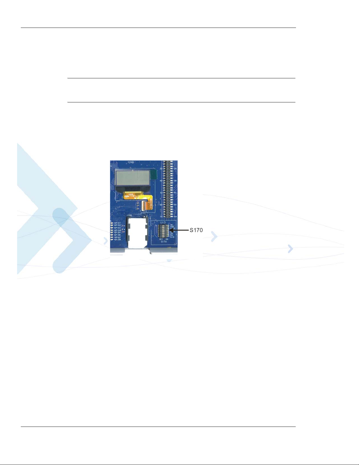
2-20 S170 Switches. . . . . . . . . . . . . . . . . . . . . . . . . . . . . . . . . . . . . . . . . . . . . . . . . . . . . . . . . . . . . . 30
2-21 S140 Switches. . . . . . . . . . . . . . . . . . . . . . . . . . . . . . . . . . . . . . . . . . . . . . . . . . . . . . . . . . . . . . 31
2-22 S141 Switches. . . . . . . . . . . . . . . . . . . . . . . . . . . . . . . . . . . . . . . . . . . . . . . . . . . . . . . . . . . . . . 32
2-23 S100 Switches. . . . . . . . . . . . . . . . . . . . . . . . . . . . . . . . . . . . . . . . . . . . . . . . . . . . . . . . . . . . . . 32
2-24 70-pin Connectors. . . . . . . . . . . . . . . . . . . . . . . . . . . . . . . . . . . . . . . . . . . . . . . . . . . . . . . . . . . 34
2-25 Jumpers and Switches on Developer Board . . . . . . . . . . . . . . . . . . . . . . . . . . . . . . . . . . . . . . . 40
2-26 LEDs on Developer Board . . . . . . . . . . . . . . . . . . . . . . . . . . . . . . . . . . . . . . . . . . . . . . . . . . . . 42
December 15, 2009 G30 Developer’s Kit iii
Page 8

List of Tables
1-1 G30 Developer’s Kit Package Contents. . . . . . . . . . . . . . . . . . . . . . . . . . . . . . . . . . . . . . . . . . . 3
2-1 Wall Mount Adapter Connector Pinout (J210). . . . . . . . . . . . . . . . . . . . . . . . . . . . . . . . . . . . . 17
2-2 Power Source Jumpers (P203, P204) . . . . . . . . . . . . . . . . . . . . . . . . . . . . . . . . . . . . . . . . . . . . 19
2-3 G30 Power Jumpers (P200, P201) . . . . . . . . . . . . . . . . . . . . . . . . . . . . . . . . . . . . . . . . . . . . . . 19
2-4 RS232-1 Connector Pinout (J300) . . . . . . . . . . . . . . . . . . . . . . . . . . . . . . . . . . . . . . . . . . . . . . 20
2-5 RS232-2 Connector Pinout (J330) . . . . . . . . . . . . . . . . . . . . . . . . . . . . . . . . . . . . . . . . . . . . . . 21
2-6 Speaker Connector Pinout (J430). . . . . . . . . . . . . . . . . . . . . . . . . . . . . . . . . . . . . . . . . . . . . . . 23
2-7 Microphone Connector Pinout (J460) . . . . . . . . . . . . . . . . . . . . . . . . . . . . . . . . . . . . . . . . . . . 23
2-8 Headset Connector Pinout (J440). . . . . . . . . . . . . . . . . . . . . . . . . . . . . . . . . . . . . . . . . . . . . . . 23
2-9 Audio Source Selection (S140-"AUDIO"). . . . . . . . . . . . . . . . . . . . . . . . . . . . . . . . . . . . . . . . 24
2-10 Voltage Level Settings for A/D Switches (J161) . . . . . . . . . . . . . . . . . . . . . . . . . . . . . . . . . . . 28
2-11 A/D Selection Switch Settings (J160) . . . . . . . . . . . . . . . . . . . . . . . . . . . . . . . . . . . . . . . . . . . 28
2-12 GPIO Signals Mapping. . . . . . . . . . . . . . . . . . . . . . . . . . . . . . . . . . . . . . . . . . . . . . . . . . . . . . . 29
2-13 S140 Switches Functionality . . . . . . . . . . . . . . . . . . . . . . . . . . . . . . . . . . . . . . . . . . . . . . . . . . 31
2-14 SIM Connector Pinout (J100). . . . . . . . . . . . . . . . . . . . . . . . . . . . . . . . . . . . . . . . . . . . . . . . . . 33
2-15 Developer Board Connectors . . . . . . . . . . . . . . . . . . . . . . . . . . . . . . . . . . . . . . . . . . . . . . . . . . 36
2-16 Developer Board Switches and Jumpers . . . . . . . . . . . . . . . . . . . . . . . . . . . . . . . . . . . . . . . . . 41
2-17 Developer Board LED Indicators. . . . . . . . . . . . . . . . . . . . . . . . . . . . . . . . . . . . . . . . . . . . . . . 43
3-1 Troubleshooting . . . . . . . . . . . . . . . . . . . . . . . . . . . . . . . . . . . . . . . . . . . . . . . . . . . . . . . . . . . . 46
iv G30 Developer’s Kit December 15, 2009
Page 9

Preface
Manual Scope
The G30 Developer’s Kit is designed to support the hardware and software development and
validation of the G30/G30 Adapter Quad Band GSM module.
This is done by routing the G30 81 pins to the “24” family 70 pin connector interface, to provide
quick interface with the “24” family Evaluation Board.
This manual describes the use of G30 Adapter Board or the G30 itself (70 pin interface connector
model) with the G30 Developer's Kit, and describes the technical details required by the user to
successfully integrate the Motorola G30 cellular engine into an original equipment manufacturer
(OEM) wireless host device. With the help of this manual, the user can utilize the Developer's Kit
to conduct a full series of test and evaluation procedures on the G30, as well as perform
application development.
Target Audience
This manual is intended for all members of the integration team who are responsible for
integrating the G30 into the host application, including representatives from hardware, software
and RF engineering disciplines.
Manual Organization
This manual contains the following chapters:
• Chapter 1—introduces the G30 Developer’s Kit
• Chapter 2—describes the Developer Board and its components in detail, including
connectors, jumpers, switches and LED indicators. It also includes a set of setup procedures
for first-time use
• Chapter 3—provides contact information for Motorola Service Support and Customer
Assistance
Applicable Documents
• G30 Module Hardware Description: 6802986C55-A
• G30 AT Commands: 6802986C33-A
December 15, 2009 G30 Developer’s Kit v
Page 10

Developer Board Safety
Developer Board Safety
Precautions
Most Developer Board circuits are not shielded. Be sure to take appropriate precautionary
measures in order to avoid ESD while handling the kit. ESD can damage the Developer Board
and/or the G30 module attached to it, using the G30 Adapter Board.
User Operation
Do not operate your unit when a person is within eight inches (20 centimeters) of the antenna. A
person or object within eight inches (20 centimeters) of the antenna could impair call quality and
may cause the unit to operate at a higher power level than necessary, as well as expose that person
to RF energy in excess of that established by the FCC RF Exposure Guidelines.
Important: The unit must be installed in a manner that provides a minimum separation distance
of eight inches (20 centimeters) or more between the antenna and persons and must
not be co-located or operate in conjunction with any other antenna or transmitter in
order to satisfy FCC RF exposure requirements for mobile transmitting devices.
Contact Us
Important: T o comply with the FCC RF exposure limits and to satisfy the categorical exclus ion
requirements for mobile transmitters, the requirements described in the following
section, “Antenna Installation” , must be met.
Antenna Installation
• A minimum separation distance of eight inches (20 centimeters) must be maintained between
the antenna and all persons.
• The combined cable loss and antenna gain must not exceed +7.5 dBi (850 band). The
combined cable loss and antenna gain must not exceed +2.5 dBi and total system output must
not exceed 2.0W EIRP in the PCS (1900) band in order to comply with the EIRP limit of
24.232 (b). OEM installers must be provided with antenna installation instruction and
transmitter operating conditions for satisfying RF exposure compliance.
We at Motorola want to make this guide as helpful as possible. Keep us informed of your
comments and suggestions for improvements.
For general contact, technical support, report documentation errors and to order manuals, use this
email address:
[email protected]
Motorola appreciates feedback from the users of our information.
vi G30 Developer’s Kit December 15, 2009
Page 11

Text Conventions
The following special paragraphs are used in this guide to point out information that must be read.
This information may be set-off from the surrounding text, but is always preceded by a bold title
in capital letters:
Note
Note: Presents additional, helpful, noncritical information that you can use.
Warning
Warning: Presents information to warn you of a potentially hazardous situation in which there
Important
Preface
is a possibility of personal injury.
Important: Presents information to help you avoid an undesirable situation
Caution
Caution: Presents information to identify a situation in which damage to software, stored
Field Service
For Field Service requests, use this email address:
[email protected]
General Safety
Remember!. . . safety depends on you!
or provides additional information to help you understand a topic or concept.
data, or equipment could occur, thus avoiding
the damage.
The following general safety precautions must be observed during all phases of operation,
service, and repair of the equipment described in this manual. Failure to comply with these
precautions or with specific warnings elsewhere in this manual violates safety standards of
design, manufacture, and intended use of the equipment. Motorola, Inc. assumes no liability for
the customer’s failure to comply with these requirements. The safety precautions listed below
represent warnings of certain dangers of which we are aware. You, as the user of this product,
December 15, 2009 G30 Developer’s Kit vii
Page 12

General Safety
should follow these warnings and all other safety precautions necessary for the safe operation of
the equipment in your operating environment.
Ground the instrument
To minimize shock hazard, the equipment chassis and enclosure must be connected to an
electrical ground. If the equipment is supplied with a three-conductor AC power cable, the power
cable must be either plugged into an approved three-contact electrical outlet or used with a
three-contact to two-contact adapter. The three-contact to two-contact adapter must have the
grounding wire (green) firmly connected to an electrical ground (safety ground) at the power
outlet. The power jack and mating plug of the power cable must meet International
Electrotechnical Commission (IEC) safety standards.
Note: Refer to “Grounding Guideline for Cellular Radio Installations”–Motorola part no.
68P081150E62.
Do not operate in an explosive atmosphere
Do not operate the equipment in the presence of flammable gases or fumes. Operation of any
electrical equipment in such an environment constitutes a definite safety hazard.
Do not service or adjust alone
Do not attempt internal service or adjustment unless another person, capable of rendering first aid
is present.
Keep away from live circuits
Operating personnel must:
• not remove equipment covers. Only Factory Authorized Service Personnel or other qualified
maintenance personnel may remove equipment covers for internal subassembly, or
component replacement, or any internal adjustment
• not replace components with power cable connected. Under certain conditions, dangerous
voltages may exist even with the power cable removed
• always disconnect power and discharge circuits before touching them
Do not substitute parts or modify equipment
Because of the danger of introducing additional hazards, do not install substitute parts or perform
any unauthorized modification of equipment. Contact Motorola Warranty and Repair for service
and repair to ensure that safety features are maintained.
Dangerous procedure warnings
Warnings, such as the example below, precede potentially dangerous procedures throughout this
manual. Instructions contained in the warnings must be followed. You should also employ all
viii G30 Developer’s Kit December 15, 2009
Page 13

Preface
other safety precautions that you deem necessary for the operation of the equipment in your
operating environment.
Warning example
Warning: Dangerous voltages, capable of causing death, are present in this equipment. Use
:
extreme caution when handling, testing,
and adjusting.
Caring for the Environment
The following information is provided to enable regulatory compliance with the European Union
(EU) Directive 2002/96/EC Waste Electrical and Electronic Equipment (WEEE) when using
Motorola equipment in EU countries.
Disposal of Motorola equipment in EU countries
Please do not dispose of Motorola equipment in landfill sites.
In the EU, Motorola in conjunction with a recycling partner will ensure that equipment is
collected and recycled according to the requirements of EU environmental law.
Please contact the Customer Network Resolution Center (CNRC) for assistance. The 24 hour
telephone numbers are listed at
http://mynetworksupport.motorola.com
Select Customer Network Resolution Center contact information.
Alternatively if you do not have access to CNRC or the internet, contact the Local Motorola
Office.
Disposal of Motorola equipment in non-EU countries
In non-EU countries, dispose of Motorola equipment in accordance with national and regional
regulations.
December 15, 2009 G30 Developer’s Kit ix
Page 14

Limitation of Liability
$UWLFOH RI WKH
(XURSHDQ 8QLRQ (8 'LUHFWLYH (& :DVWH (OHFWULFDO DQG (OHFWURQLF
(TXLSPHQW :(((
7KH *RYHUQPHQW RI 7XUNH\ UHTXHVWV D VWDWHPHQW RI FRQIRUPLW\ ZLWK WKH ((( UHJXODWLRQ
EH SURYLGHG ZLWK WKLV HTXLSPHQW 7KLV VWDWHPHQW RI ((( FRQIRUPLW\ LQ 7XUNLVK LV (((
<|QHWPHOL÷LQH 8\JXQGXU
Turkey
Limitation of Liability
The Products are not designed, intended, or authorized for use as components in systems intended
for surgical implant into the body; in other applications intended to support or sustain life; for the
planning, construction, maintenan ce, operation or use of any nuclear facility; for the flight,
navigation, communication of aircraft or ground support equipment; or in any other application in
which the failure of the Product could create a situation where personal injury or death may occur.
If CUSTOMER should use any Product or provide any Product to a third party for any such use,
CUSTOMER hereby agrees that MOTOROLA is not liable, in whole or in part, for any claims or
damages arising from such use, and further agrees to indemnify and hold MOTOROLA harmless
from any claim, loss, cost or damage arising from such use.
EXCEPT AS SPECIFICALLY STATED ABOVE, THE PRODUCTS ARE PROVIDED "AS IS"
AND MOTOROLA MAKES NO OTHER WARRANTIES EXPRESS, IMPLIED,
STATUTORY, OR OTHERWISE REGARDING THE PRODUCTS. MOTOROLA
SPECIFICALLY DISCLAIMS ANY IMPLIED WARRANTIES OF MERCHANTABILITY
AND FITNESS FOR A PARTICULAR PURPOSE, OR ARISING FROM A COURSE OF
DEALING OR USAGE OF TRADE.
Under no circumstances shall MOTOROLA be liable to CUSTOMER or any other par t y fo r any
costs, lost revenue or profits or for any other special, incidental or consequential damages, even if
MOTOROLA has been informed of such potential loss or damage. And in no event shall
MOTOROLA's liability to CUSTOMER for damages of any nature exceed the total purchase
price CUSTOMER paid for the Product at issue in the dispute, except direct damages resulting
from patent and/or copyright infringement, which shall be governed by the "INDEMNITY"
Section of this Agreement.
The preceding states MOTOROLA's entire liability for MOTOROLA's breach or failure to
perform under any provision of this Agreement.
Warranty Notification
Motorola guarantees to you, the original purchaser, the OEM Module and accessories which you
have purchased from an authorized Motorola dealer (the "Products"), to be in conformance with
the applicable Motorola specifications current at the time of manufacture for a term of fifteen (15)
months from Product manufacture date (Warranty Term).
You must inform Motorola of the lack of conformity to the applicable specifications of any of the
Products within a period of two (2) months from the date on which you detect a defect in
material, workmanship or lack of conformity and in any event within a term not to exceed the
Warranty Term, and must immediately submit the Product for service to Motorola's Authorized
Repair or Service Center. Motorola shall not be bound by Product related statements not directly
made by Motorola nor any warranty obligations applicable to the seller.
A list of the Motorola Call Center numbers is enclosed with this Product.
x G30 Developer’s Kit December 15, 2009
Page 15

Preface
During the Warranty term, Motorola will, at its discretion and without extra charge, as your
exclusive remedy, repair or replace your Product which does not comply with this warranty; or
failing this, to reimburse the price of the Product but reduced to take into account the use you
have had of the Product since it was delivered. This warranty will expire at the end of the
Warranty Term.
This is the complete and exclusive warranty for a Motorola OEM Module and accessories and in
lieu of all other warranties, terms and conditions, whether express or implied.
Where you purchase the product other than as a consumer, Motorola disclaims all other
warranties, terms and conditions express or implied, such as fitness for purpose and satisfactory
quality.
In no event shall Motorola be liable for damages nor loss of data in excess of the purchase price
nor for any incidental special or consequential damages* arising out of the use or inability to use
the Product, to the full extent such may be disclaimed by law.
This Warranty does not affect any statutory rights that you may have if you are a consumer, such
as a warranty of satisfactory quality and fit for the purpose for which products of the same type
are normally used under normal use and service, nor any rights against the seller of the Products
arising from your purchase and sales contract.
(*)including without limitation loss of use, loss of time, loss of data, inconvenience, commercial
loss, lost profits or savings.
How to Get Warranty Service?
In most cases the authorized Motorola dealer which sold and/or installed your Motorola OEM
Module and original accessories will honor a warranty claim and/or provide warranty service.
Alternatively, for further information on how to get warranty service please contact either the
customer service department of your service provider or Motorola's service centers, listed in
Chapter 3.
Claiming
In order to claim the warranty service you must return the OEM Module and/or accessories in
question to Motorola's Authorized Repair or Service Center in the original configuration and
packaging as supplied by Motorola. Please avoid leaving any supplementary items like SIM
cards. The Product should also be accompanied by a label with your name, address, and telephone
number; name of operator and a description of the problem.
In order to be eligible to receive warranty service, you must present your receipt of purchase or a
comparable substitute proof of purchase bearing the date of purchase. The phone should also
clearly display the original compatible electronic serial number (IMEI) and mechanic serial
number [MSN]. Such information is contained with the Product.
You must ensure that all and any repairs or servicing is handled at all times by a Motorola
Authorized Service Center in accordance with the Motorola Service requirements
In some cases, you may be requested to provide additional information concerning the
maintenance of the Products by Motorola Authorized Service Centers only, therefore it is
important to keep a record of any previous repairs, and make them available if questions arise
concerning maintenance
December 15, 2009 G30 Developer’s Kit xi
Page 16

Conditions
Conditions
This warranty will not apply if the type or serial numbers on the Product has been altered, deleted,
duplicated, removed, or made illegible. Motorola reserves the right to refuse free-of-charge
warranty service if the requested documentation can not be presented or if the information is
incomplete, illegible or incompatible with the factory records.
Repair, at Motorola's option, may include reflashing of software, the replacement of parts or
boards with functionally equivalent, reconditioned or new parts or boards. Replaced parts,
accessories, batteries, or boards are warranted for the balance of the original warranty time
period. The Warranty Term will not be extended. All original accessories, batteries, parts, and
OEM Module equipment that have been replaced shall become the property of Motorola.
Motorola does not warrant the installation, maintenance or service of the products, accessories,
batteries or parts.
Motorola will not be responsible in any way for problems or damage caused by any ancillary
equipment not furnished by Motorola which is attached to or used in connection with the
Products, or for operation of Motorola equipment with any ancillary equipment and all such
equipment is expressly excluded from this warranty.
When the Product is used in conjunction with ancillary or peripheral equipment not supplied by
Motorola, Motorola does not warrant the operation of the Product/peripheral combination and
Motorola will not honor any warranty claim where the Product is used in such a combination and
it is determined by Motorola that there is no fault with the Product. Motorola specifically
disclaims any responsibility for any damage, whether or not to Motorola equipment, caused in
any way by the use of the OEM Module, accessories, software applications and peripherals
(specific examples include, but are not limited to: batteries, chargers, adapters, and power
supplies) when such accessories, software applications and peripherals are not manufactured and
supplied by Motorola.
What is Not Covered by the Warranty
This warranty is not valid if the defects are due to damage, misuse, tampering, neglect or lack of
care and in case of alterations or repair carried out by unauthorized persons.
The following are examples of defects or damage not covered by this product warranty
1. Defects or damage resulting from use of the Product in other than its normal and custom ary
manner.
2. Defects or damage from misuse, access to incompatible sources, accident or neglect.
3. Defects or damage from improper testing, operation, maintenance, installation, adjustment,
unauthorized software applications or any alteration or modification of any kind.
4. Breakage or damage to antennas unless caused directly by defects in material or
workmanship.
5. Products disassembled or repaired other than by Motorola in such a manner as to adversely
affect performance or prevent adequate inspection and testing to verify any warranty claim.
6. Defects or damage due to range, coverage, availability, grade of service, or operation of the
cellular system by the cellular operator.
7. Defects or damage due to moist, liquid or spills of food.
8. Control unit coil cords in the Product that are stretched or have the modular tab broken.
xii G30 Developer’s Kit December 15, 2009
Page 17

9. All plastic surfaces and all other externally exposed parts that are scratched or damaged due
Depending on operating conditions and your usage habits, wear and tear might take place of
components including mechanical problems related to Product housing, paint, assembly,
sub-assemblies, displays and keyboards and any accessories which are not part of the Product's
in-box configuration. The rectification of faults generated through wear and tear and the use of
consumable items like batteries beyond their Optimum Performance Time as indicated in the
product manual is considered to be your responsibility and therefore Motorola will not provide
the free Warranty repair service for these items
Installed Data
Please make and retain a note of all data you have inserted into your Product for example names,
addresses, phone numbers, user and access codes, notes etc. before submitting your Product for a
Warranty service as such data may be deleted or erased as part of the repair or service process.
Please note if you have downloaded material onto your Product, these may be deleted or erased as
part of the repair process or testing process. Motorola shall not be responsible for such matters.
The repair or testing process should not affect any such material that was installed by Motorola
on your Product as a standard feature.
Preface
to customer normal use.
Out of Warranty Repairs
If you request Motorola to repair your Product any time after the Warranty term or where this
warranty does not apply due to the nature of the defect or fault, then Motorola may in its
discretion carry out such repairs subject to you paying Motorola its fees for such a repair or it may
refer you to an authorized third party to carry out such repairs.
December 15, 2009 G30 Developer’s Kit xiii
Page 18
Revision History
Revision History
Manual Number
6802986C48
Manual Title
G30 Developer’s Kit
Version Information
The following table lists the manual version, date of version, and remarks about the version
required.
Revision History
Version Date Issue Remarks
A December 15, 2009 Initial Release
xiv G30 Developer’s Kit December 15, 2009
Page 19
Chapter 1: Introduction
SIM Tray
On-board Antenna
General Description
The G30 Developer’s Kit is intended for evaluating the G30 module, as well as for developing
and testing software applications for it.
The main component of the G30 Developer’s Kit is the Developer Board, which is mounted in a
chassis. The kit includes a cover for the Developer Board. The cover has openings on the top and
sides to accommodate the Developer Board’s external connectors.
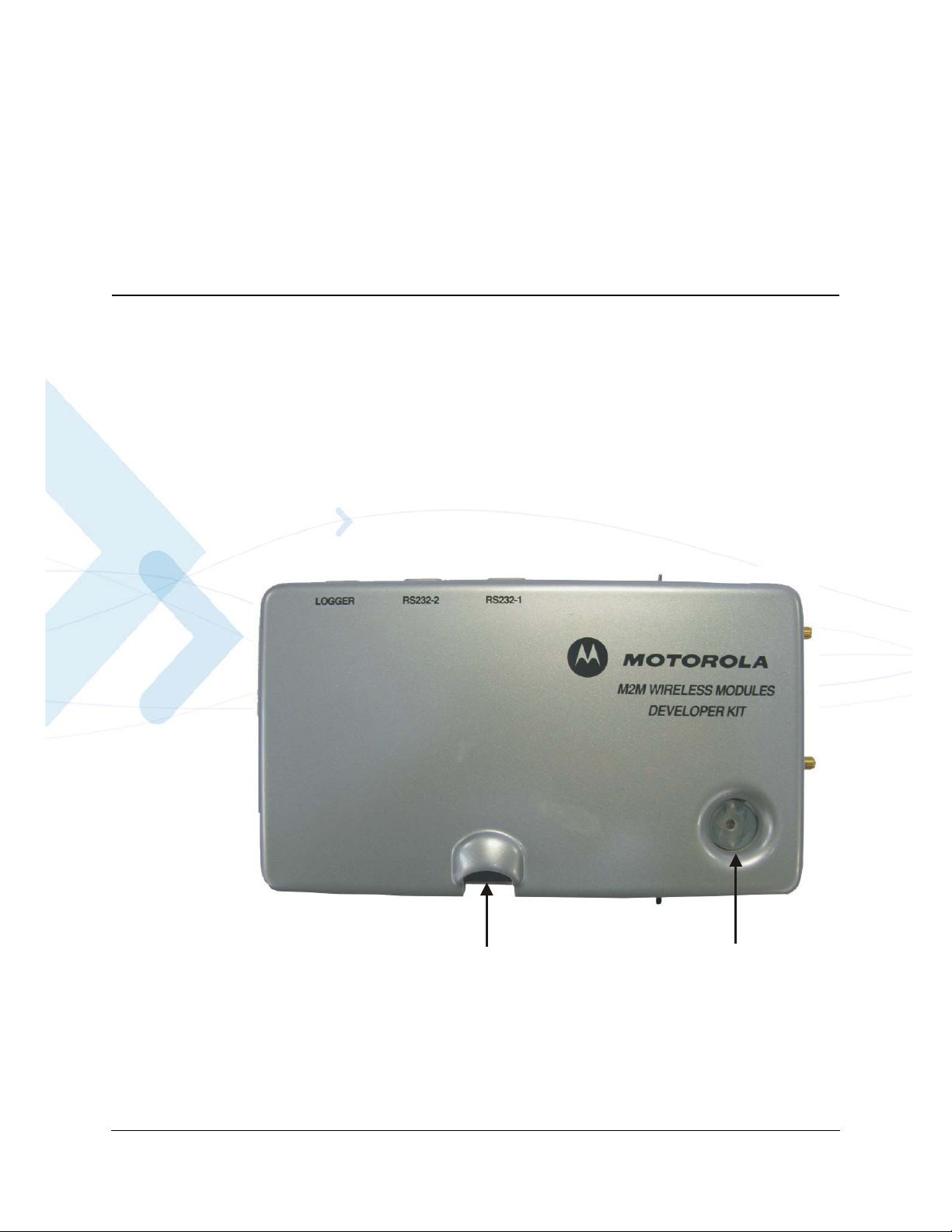
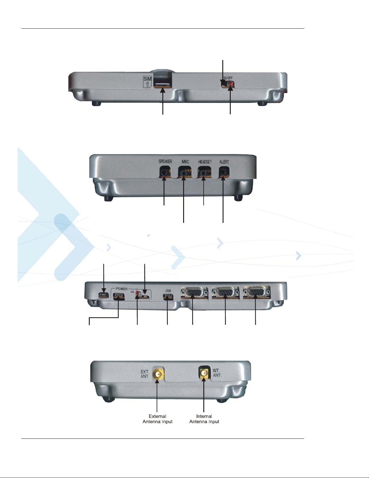
Figure 1-1 shows the Developer’s Kit top view with cover; Figure 1-2 shows the front view;
Figure 1-3 shows the left side view; Figure 1-4 shows the rear view; Figure 1-5 shows the right
side view.
Figure 1-1: G30 Developer’s Kit—Top View with Cover
December 15, 2009 G30 Developer’s Kit 1
Page 20
General Description
SIM Tray G30 On/Off
Pushbutton
G30 Power
Indicator
Speaker
Connector
NA For
G30
Headset
Connector
Microphone
Connector
NA For
G30
NA For
G30
RS232-2
Connector
RS232-1
Connector
Power
On/Off Switch
Power
Indicator LED
For Development
Use Only
Wall-mount
Adapter Connector
Figure 1-2: G30 Developer’s Kit—Front View with Cover
Figure 1-3: G30 Developer’s Kit—Left Side View with Cover
Figure 1-4: G30 Developer’s Kit—Rear View with Cover
2 G30 Developer’s Kit December 15, 2009
Figure 1-5: G30 Developer’s Kit—Right Side View with Cover
Page 21
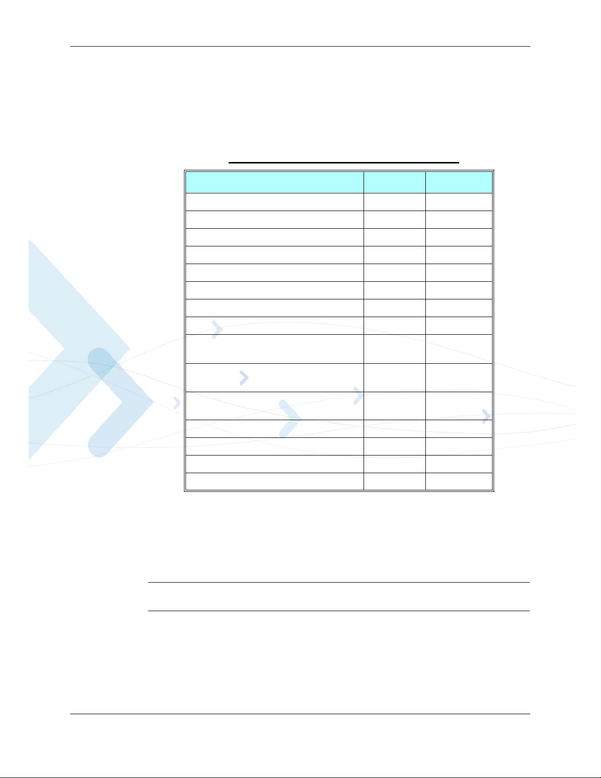
Package Contents
The G30 Developer’s Kit includes the Developer Board, chassis, cover and standard accessories,
which enable you to better utilize the board. The kit and its components are described in
Table 1-1.
Antenna Stub 8588912N02 1
Developer Board FCN5540C 1
Developer Board Top Cover 1588522V58 1
Developer Board Bottom Cover 1588522V59 1
Documentation CD FVN5423A 1
European Plug for Adapter SYN7456A 1
M2/6mm Screw (for G30 fastening) 0387839V09 2
Table 1-1: G30 Developer’s Kit Package Contents
Description Part No. Quantity
Mono Headset SYN8390B 1
RF cable between internal antenna and
external connectors
RF cable with MMCX connector between
G30 and external antenna connector
RF cable with U.FL connector between
G30 and external antenna connector
RS232 Cable 3086159U69 1
Test SIM Card 8102316T02 1
Mini-AB USB Cable (not used with G30) SKN6371B 1
Wall Mount Power Adapter SPN5202A 1
3087568V01 1
3087568V02 1
3087568V99 1
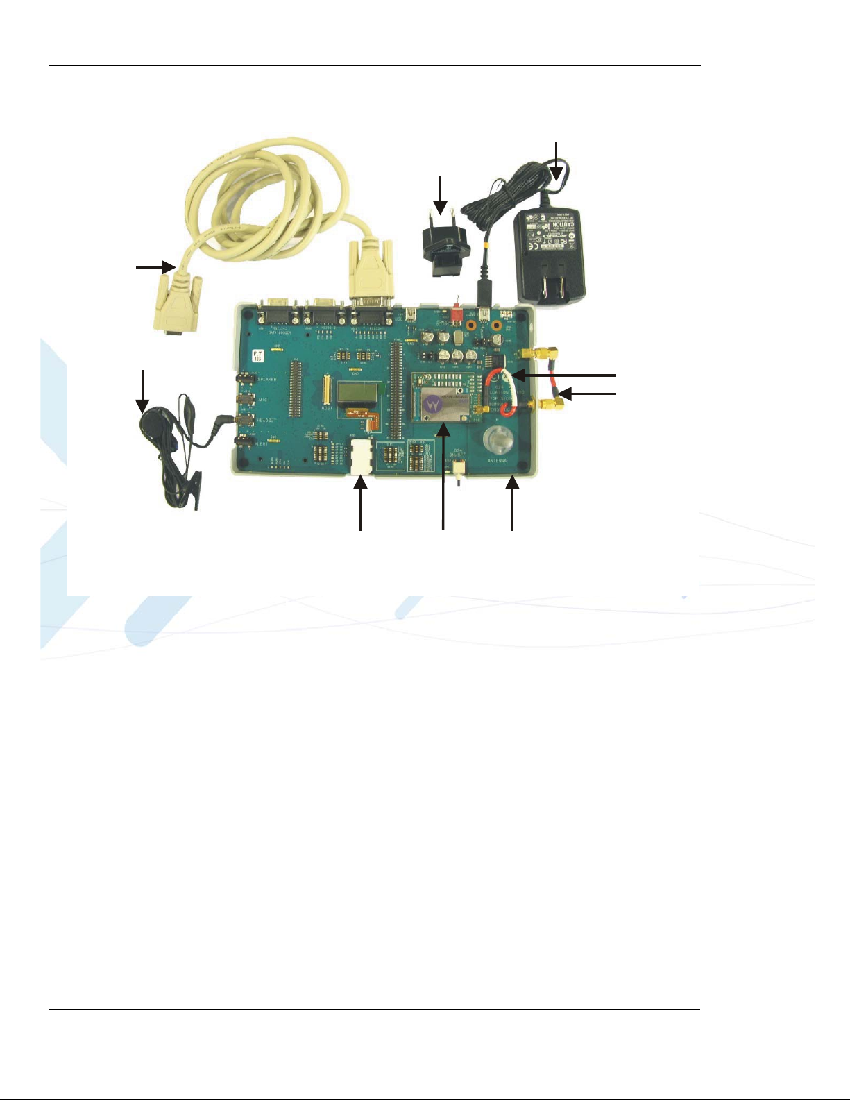
Figure 1-6 shows the G30 Developer’s Kit, including the Developer Board (without cover), the
G30 Adapter and some accessories.
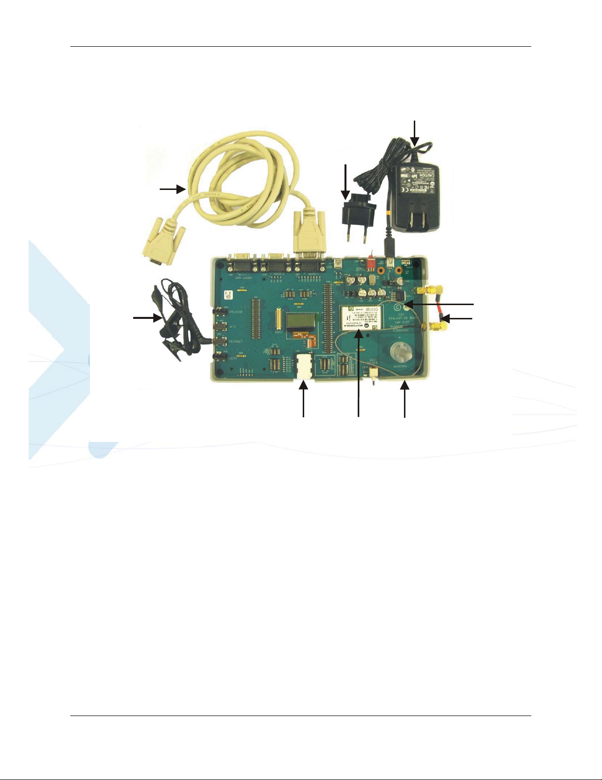
Figure 1-7 shows the G30 Developer’s Kit, including the Developer Board (without cover), the
G30 and some accessories.
Important: The Developer’s Kit does not include a G30/G30 Adapter device. The G30/G30
Adapter must be obtained separately.
December 15, 2009 G30 Developer’s Kit 3
Page 22
Package Contents
RS232
Cable
Headset
G30
Adapter
Developer
Board
SIM
Card
RF
Cables
Power
Adapter
Adapter Plug
Figure 1-6: G30 Developer’s Kit with Board, G30 Adapter and Accessories
4 G30 Developer’s Kit December 15, 2009
Page 23
RS232
Cable
Headset
G30
Developer
Board
SIM
Card
RF
Cables
Wall-mount
Power
Adapter
Adapter Plug
Figure 1-7: G30 Developer’s Kit with Board, G30 and Accessories
December 15, 2009 G30 Developer’s Kit 5
Page 24

Package Contents
This page intentionally left blank.
6 G30 Developer’s Kit December 15, 2009
Page 25

Chapter 2: Developer Board and Interfaces Description
This chapter contains the following sections:
• Overview—provides an overview of the Developer Board
• Initial Setup—describes how to set up and prepare the Developer Board for first-time use
• Configuration—describes how to modify the default settings to control the operation of the
Developer Board
• Components and Specifications—l ists each connector, switch, jumper, option switch.
and LED. Also provides other details and specifications for the Developer Board
Overview
The G30 Developer Board is designed to support the hardware and software development and
validation of the G30 GSM/GPRS/EGPRS data module. The Developer Board provides a
peripheral platform to operate the G30 as a standalone product, and to easily access the G30
70-pin interface connector signals.
Developer Board Features and Structure
The Developer Board provides these features to facilitate software and hardware development:
• Easy access to G30 70-pin interface connector signals, through a large header connector and
an external host connector
• Wall adapter and DC power supplies for board operation
• LED indicators for critical signals
• RS232 serial interfaces
• Analog audio interface for speaker, alert speaker, microphone and headset
• SIM card interface
• Switches and jumpers for controlling board operat ion
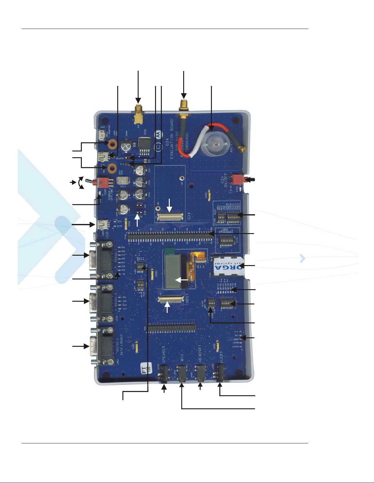
Figure 2-1 shows the Developer Board structure:
December 15, 2009 G30 Developer’s Kit 7
Page 26
Overview
On-board
Antenna
SIM Card
Tray
G30 On/Off
Pushbutton
GPIO
LEDs
GPIO
Switches
ADC
Switches
G30 Header
Connector
General
LEDs
General
Switches
G30 UUT
Connector
Power
Jumpers
Host
Connector
Display
External
Antenna
Input
Power
Source
Jumpers
Internal
Antenna
Input
Wall
Adapter
Connector
Speaker
Connector
RS232-1
LEDs
RS232-1
Connector
RS232-2
Connector
Power On/Off
Switch
DC Power
Connectors
(Not Included)
Power Indicator
LED
Microphone
Connector
Headset
Connector
On
Off
NA for
G30
NA for
G30
NA for
G30
NA for
G30
Figure 2-1: Developer Board Structure
8 G30 Developer’s Kit December 15, 2009
Page 27

Initial Setup
Chapter 2: Developer Board and Interfaces Description
This section describes the initial procedure for setting up the Developer Board for G30 testing
and evaluation. The tasks in this section need to be performed only once, prior to initial use of the
Developer’s Kit. After performing the initial setup, you can modify the default settings or use
different peripheral devices, as described in “Configuration” on page 16.
Perform the steps in this section in sequence.
Before starting, remove the cover of the Developer Board. The cover simply slides up off the
board, and does not require the removal of any screws or clips. After setting up the Developer
Board, replace the cover simply by pushing it gently back into place. Make sure the cover is
aligned properly with the external connectors on the side of the board.
Note: Numbers that appear in parentheses throughout the following paragraphs (Jxxx, Sxxx,
etc.), refer to components reference designation numbers as they are given on the
developer board and in the schematic diagrams.
Connecting the G30 Adapter
To Connect the G30 Adapter to the Developer Board
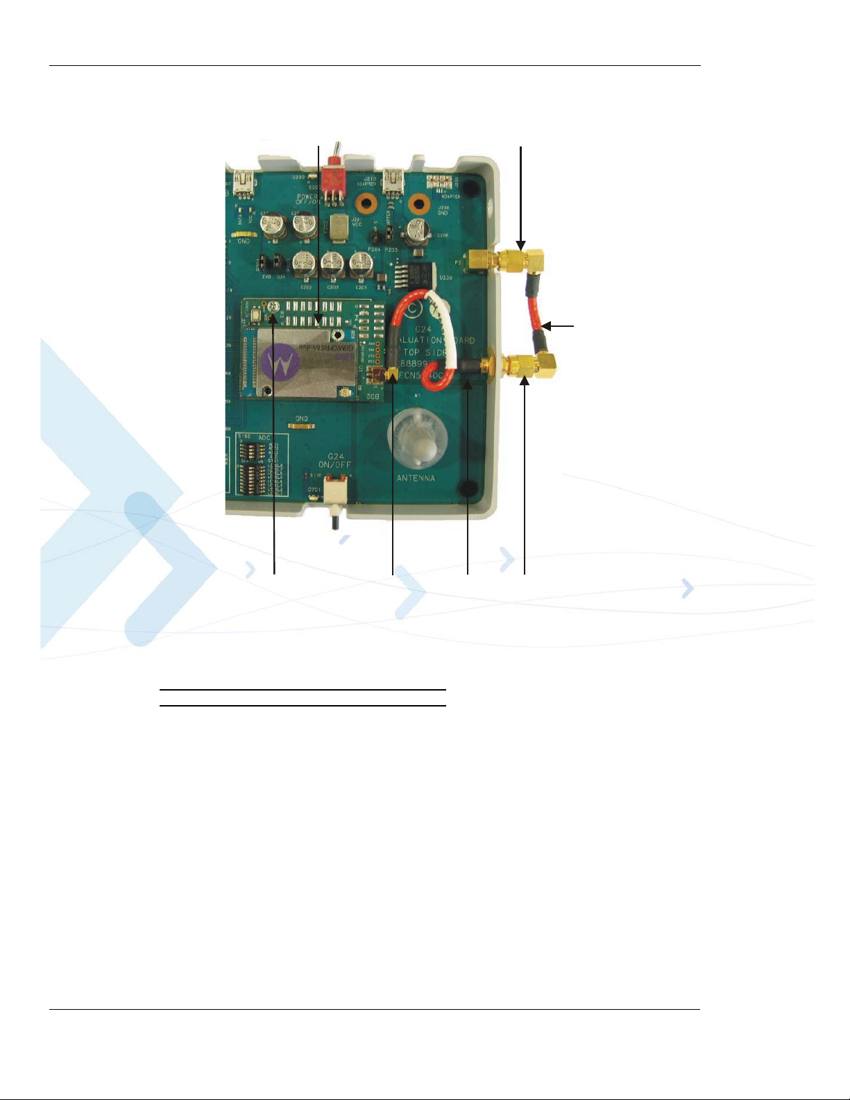
1. Place the G30 adapter (Figure 2-2) on the Developer Board area, marked by a white
rectangle, and push the G30 adapter 70-pin connector down into the G30 70-pin connector
on the Developer Board.
The screw hole on the G30 adapter should be aligned with the G30 spacer (denoted by M2).
2. Fasten the G30 adapter to the Developer Board using one M2 screw provided with the kit.
3. Connect the internal RF cable MMCX connector to the MMCX connector of the G30
adapter by pushing it in until it clicks (Figure 2-2).
4. Insert the External Antenna Connector into the dedicated hole in the Developer Board cover
and close nut.
5. Connect the external RF cable between the External Antenna Connector and the Internal
Antenna Connector (Figure 2-2).
This connects the G30 adapter to the antenna.
December 15, 2009 G30 Developer’s Kit 9
Page 28
Initial Setup
MMCX
Connector
Internal
RF Cable
External
RF Cable
External
Antenna
Connector
Internal
Antenna
Connector
G30 Adapter
G30 Adapter
Screw
.
Figure 2-2: Connecting the G30 Adapter
Connecting the G30
To Connect the G30 to the Developer Board
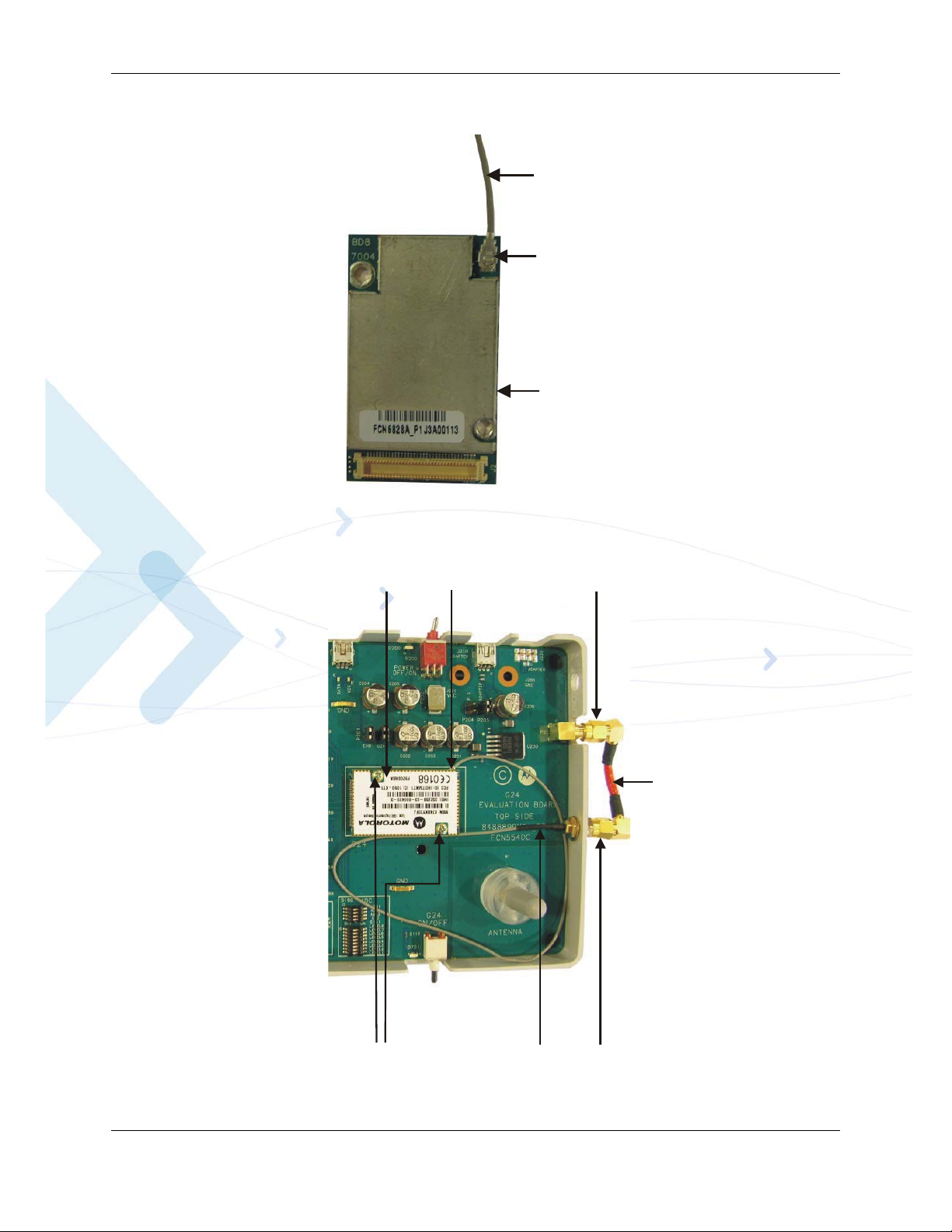
1. Connect the internal RF cable U.FL connector to the U.FL connector of the G30 by pushing
it until it clicks (Figure 2-3).
2. Place the G30 (Figure 2-4) on the Developer Board area, marked by a white rectangle, and
push the G30 70-pin connector down into the G30 70-pin connector on the Developer Board.
The two screw holes on the G30 should be aligned with the G30 spacers (denoted by M2 and
M3).
3. Fasten the G30 to the Developer Board using the two M2 screws provided with the kit.
4. Insert the External Antenna Connector into the dedicated hole in the Developer Board cover
and close nut.
5. Connect the external RF cable between the External Antenna Connector and the Internal
Antenna Connector (Figure 2-4).
This connects the G30 to the antenna.
10 G30 Developer’s Kit December 15, 2009
Page 29
Chapter 2: Developer Board and Interfaces Description
U.FL
Connector
G30 Bottom
View
Internal
RF Cable
U.FL
Connector
Internal
RF Cable
External
RF Cable
External
Antenna
Connector
Internal
Antenna
Connector
G30
G30
Screws
Figure 2-3: Connecting the U.FL Connector to the G30
.
Figure 2-4: Connecting the G30
December 15, 2009 G30 Developer’s Kit 11
Page 30
Initial Setup
Developer Board
On/Off Switch
Power
Indicator LED
Wall-mount
Adapter Connector
Connecting External Accessories
Replace the Developer Board cover and connect the following external connectors in the
sequence shown.
Power Supply
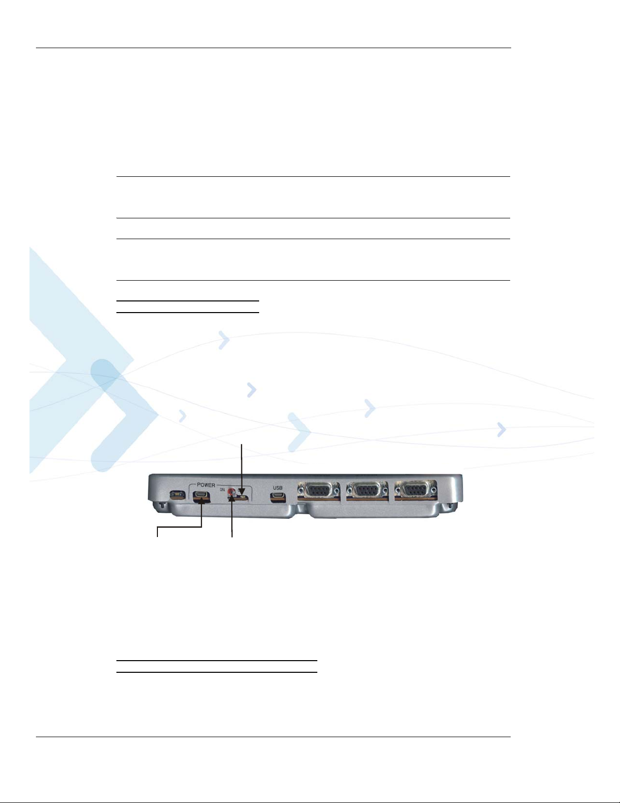
Caution: Before connecting the power supply, make sure that the Developer Board On/Off
switch (located in the rear of the board, as shown in Figure 2-5) is in the
position.
Caution: When using the Wall adapter, make sure to insert it into the Power Adapter
Connector (J210) and not to the Mini-AB USB connector (J380), as shown in
Figure 2-5.
To Connect the Power Supply
1. Connect the supplied Wall adapter to the Wall Adapter Connector (J230) (Figure 2-5).
OFF
The Wall Adapter Connector is located to the left of the Developer Board On/Off switch
(labeled
Power) at the rear of the Developer Board.
2. Plug the adapter into a wall outlet.
Note: The G30 Developer Board can also be powered by an external DC power supply. This
option is described in “Configuration” on page 16.
Figure 2-5: Developer Board Power Switch and Adapter Connector (Rear)
Serial Communications
RS232 serial interface is available for communicating with a PC. The G30 Developer’s Kit
includes the necessary RS232 cable for connecting to a PC.
12 G30 Developer’s Kit December 15, 2009
To Connect
• Connect (Figure 2-5) either the supplied RS232 cable with a male D-type connector to
Serial Communication Cables
RS232-1 connector (J300), or to the RS232-2 connector (J330) for data logging.
Page 31
Chapter 2: Developer Board and Interfaces Description
Speaker
Connector
NA For
G30
Headset
Connector
Microphone
Connector
The RS232 connector is located to the right of the Developer Board On/Off switch (labeled
Power) at the rear of the Developer Board.
Audio Devices
The G30 Developer’s Kit has connectors that support the following audio devices:
• Headset (supplied)
• Microphone
• Speaker
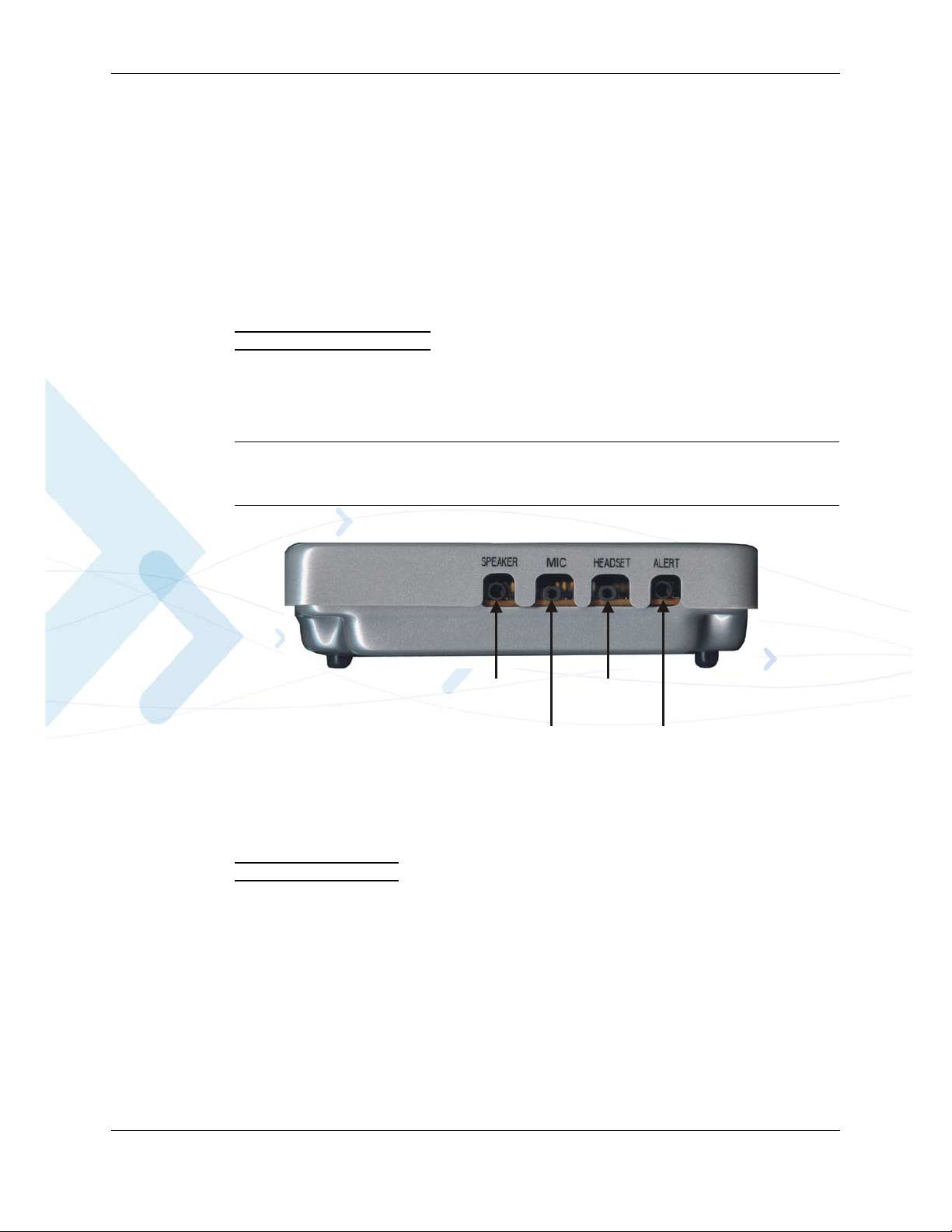
To Connect Audio Devices
• Connect the supplied headset to the appropriate connector, labeled HEADSET (Figure 2-6)
The Audio Connectors are located on the left side of the Developer’s Board.
Important: The G30 Developer Board enables connection of additional audio devices, which
are not supplied with the Developer Kit. These devices are described in
“Configuration” on page 16.
Figure 2-6: Audio Connectors (Left Side)
External SIM Card
To Insert the SIM Card
Note: A test SIM card is provided with the G30 Developer’s Kit.
• Insert a SIM card (Figure 2-7) into the SIM tray (J100) with the contacts down and the
cut-off corner to the front and right
December 15, 2009 G30 Developer’s Kit 13
Page 32
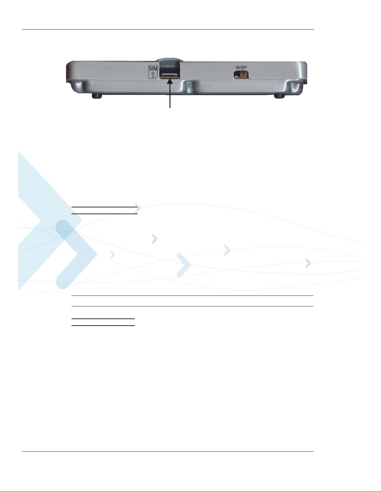
Initial Setup
SIM Tray
A diagram on the cover indicates how to insert the SIM card.
Figure 2-7: SIM Tray
Note: When using a G30 with an Embedded SIM, verify the following:
1. A SIM card is not inserted into the SIM tray.
2. G30 "ESIM_RST" and "SIM_RST" signals are shorted on the EVB. This could be
done by manually shorting P100 header pins 56 and 44.
Antenna
To Attach the Antenna
• Screw the supplied antenna into the antenna base, located at the bottom-right corner on top of
the Developer's Kit.
The Developer's Kit arrives configured to operate with its on-board internal antenna. The
EXT ANT and INT ANT connectors are connected together using an external RF cable, on
the board's right side (Figure 2-2 and Figure 2-3).
Power Up
Important: You must turn the Developer Board power on before turning on the G30.
To Turn on the Power
1. Turn on the Developer Board power by switching the power On/Off switch (S200) to ON
(Figure 2-5).
The Developer Board power On/Off switch (labeled
Developer Board.
The Developer Board power indicator LED is lit.
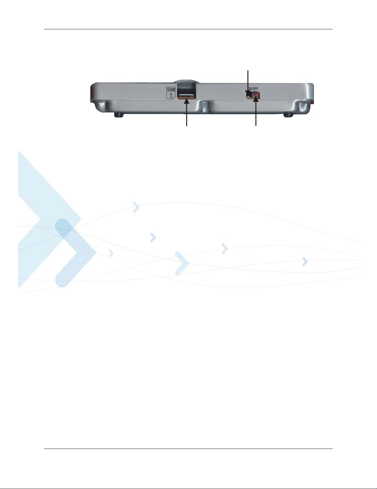
2. Turn on the G30 power by pressing the On/Off pushbutton (S110) for at least 0.5 seconds
(Figure 2-8).
Power) is located at the rear of the
The G30 power On/Off pushbutton is located at the front of the Developer Board.
14 G30 Developer’s Kit December 15, 2009
Page 33
Chapter 2: Developer Board and Interfaces Description
SIM Tray G30 On/Off
Pushbutton
G30 Power
Indicator
The G30 On/Off LED is lit.
Figure 2-8: G30 On/Off Pushbutton and Power Indicator LED
Initial Setup of the Developer Board is now complete and the board is ready for use.
December 15, 2009 G30 Developer’s Kit 15
Page 34
Configuration
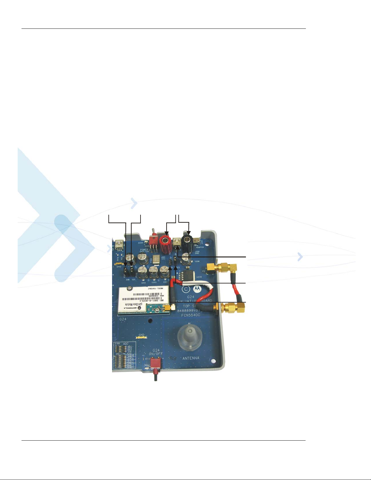
P200
(G24 Power
Jumper)
P203
(Adapter Power
Jumper)
P204
(P.S Power
Jumper)
DC Power
Connectors
(Not Included)
Wall Mount
Adapter
Connector
P201
(Developer Board
Power Jumper)
Configuration
After performing Initial Setup (previous section), you can continue using the Developer Board
this default setup. This section describes how to change the default setup so you can use different
peripherals or change default board operation.
Alternate Power Sources
The Developer Board power can be supplied from:
• Wall mount power adapter (See “Wall Mount Adapter Operation” on page 17.)
• External DC power source (See “DC Power Source Operation” on page 18.)
A single power source is used for the G30 and the board peripherals.
You must connect the Developer Board to a power source, and then set the power source jumper
(P204), if necessary (See “Selecting the Power Source” on page 19.).
Two other jumpers (Figure 2-9) help control the power supply in th e De veloper Board:
• P201—Connects/disconnects the power from the Develo per Board peripherals
• P200—Connects/disconnects the power from the G30
16 G30 Developer’s Kit December 15, 2009
Figure 2-9: Power Supply Connectors, Jumpers and Switches
Each power supply option is described in the sections that follow.
Page 35
Chapter 2: Developer Board and Interfaces Description
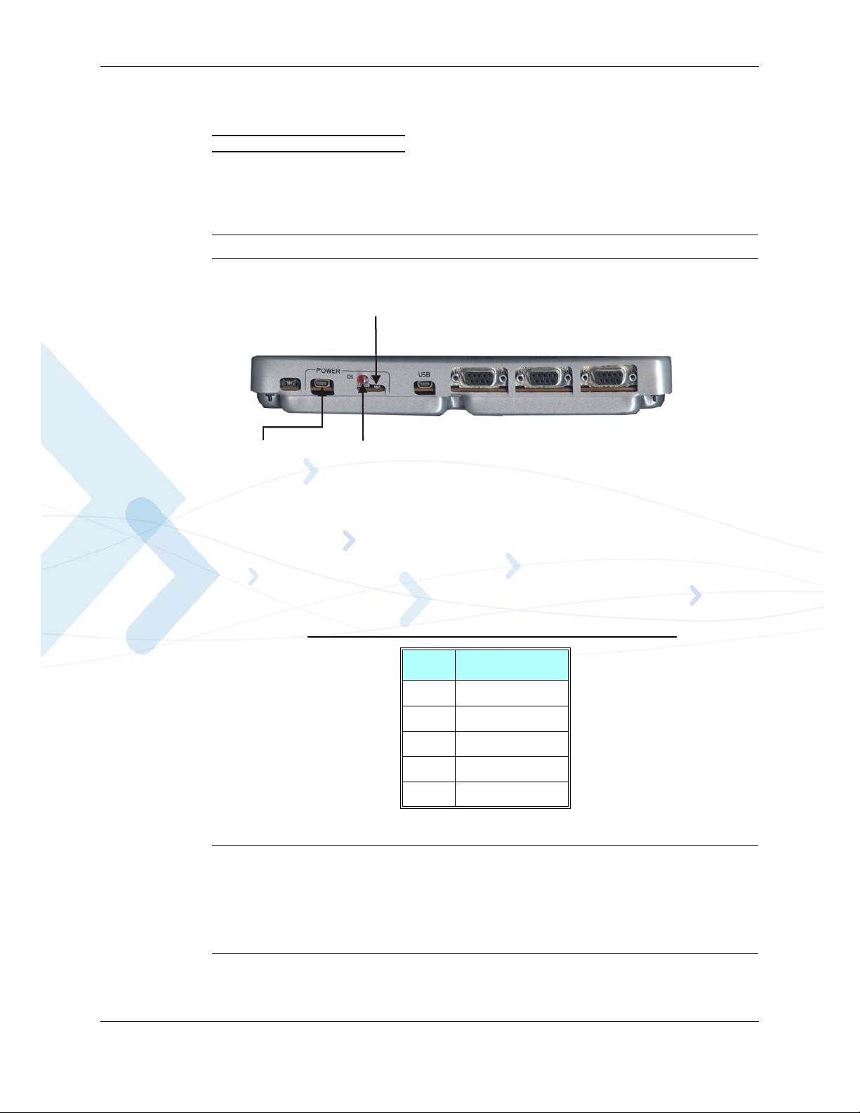
Power
On/Off Switch
Power
Indicator LED
Wall-mount
Adapter Connector
Wall Mount Adapter Operation
To Use a Wall Mount Adapter
1. Connect the Wall mount adapter to the Power Adapter connector (J210) (Figure 2-10)
2. Verify that jumper P203 is connected and jumper P204 is disconnected (default setup).
Important: Verify that the Wall mount adapter is not connected to the USB connector (J380).
Figure 2-10: G30 Developer’s Kit Wall Mount Adapter Connector
The Wall Mount Adapter connector is located at the rear of the Developer Board,
immediately to the left of the Power On/Off switch.
The Wall Mount Adapter connector pinout is described in Table 2-1. The adapter supplies a
constant 4.5 V, which is regulated to a nominal 4.1 V on the Developer Board.
Table 2-1: Wall Mount Adapter Connector Pinout (J210)
Pin # Pin Name
1 GND
2 Not connected
3 Not connected
5 Detection circuit
6 VCC
Important: The G30 includes an on-board protection circuit for cases in which the USB
connector is connected by mistake to the Wall Mount Adapter connector (J210).
If by mistake, the Mini AB USB cable is connected to J210 instead of J380, the on
board Wall mount adapter is disabled, preventing unrequired load on the host
December 15, 2009 G30 Developer’s Kit 17
computer.
Page 36
Configuration
DC Power Source Operation
To Use an External DC Power Supply
1. Remove the Developer Board cover.
When using the DC power input connectors, the Developer Board cover must be removed.
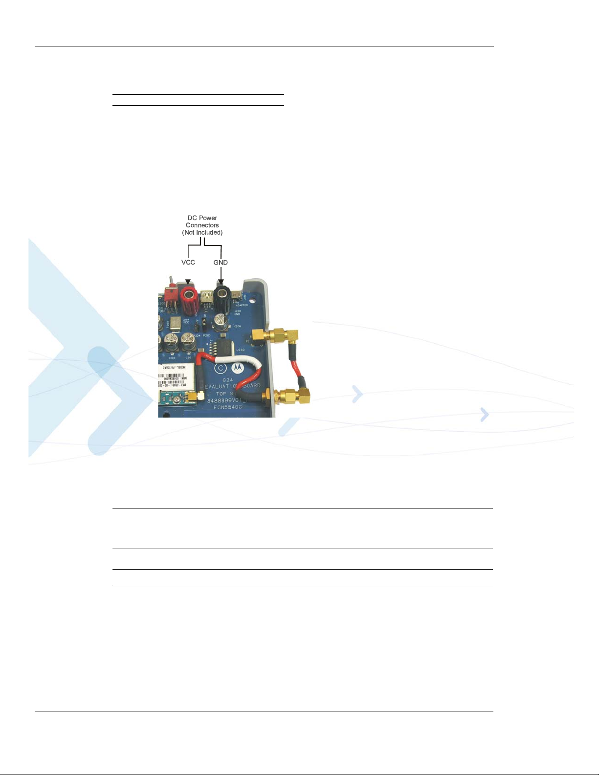
2. Attach the DC input connectors to the Developer Board (Figure 2-11).
Note: The DC input connectors are not included and should be purchased separately.
Use the red connector for
VCC and the black one for GND.
Figure 2-11: DC Input Connectors
3. Connect the external DC power supply to the
banana plugs, alligator clips or wire.
VCC (J201) and GND (J200) connectors using
4. Move jumper P203 to jumper P204.
Important: The DC voltage applied through this connection should not exceed the
recommended operational limits of 3.3 V to 4.2 V. In any case, the DC source input
is protected from over voltage and reverse polarity, and includes a protective fuse.
Important: The DC power source should not be used when other sources are connected.
18 G30 Developer’s Kit December 15, 2009
Page 37
Chapter 2: Developer Board and Interfaces Description
Selecting the Power Source
The Developer Board can be powered using two different power sources:
• Wall-mount power adapter (default source)
• External DC power supply
Important: Only one power source can be used at any given time.
T wo jumpers are used for selecting the power source - P203 for Wall-mount adapter and P204 for
the external DC power supply (Figure 2-9). The jumpers position for each power source is
described in Table 2-2.
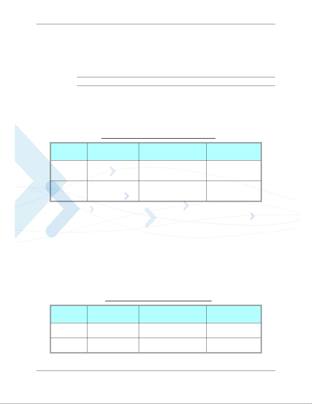
Table 2-2:
Power Source Jumpers (P203, P204)
Reference Description Jumper Connected
P203 Wall-mount adapter
power selection jumper
P204 External DC power selec-
tion power.
Wall mount adapter is used as the
power source for the G 30 Developer board.
DC power is used as the power
source for the G30 Developer
board.
Disconnecting Power
The Developer Board and G30 supplies are separated by two jumpers (P200, P201) (Figure 2-9)
that allow disconnecting the power to the Developer Board or to the G30.
Developer Board. Disconnecting power to the Developer Board is generally used to diagnose
a problem that may be caused by the board. This is independent of power supply to the G30,
which will continue to receive power. The Developer Board Power jumper (P201) (Figure 2-9)
positions for connecting and disconnecting power to the Developer Board are shown in Table 2-3.
G30. Disconnecting the power to the G30 is generally used to connect an amperometer to the
jumper’s two pins to measure the current through the G30. The G30 Power Jumper (P200)
(Figure 2-9) positions for connecting and disconnecting power to the G30 are shown in Table 2-3.
Jumper Not
Connected
Wall adapter is NOT used.
DC power is NOT used.
Table 2-3: G30 Power Jumpers (P200, P201)
Jumper Not
Reference Description Jumper Connected
P200 Connects/Disconnects
G30 power.
P201 Connects/Disconnects
Developer board power.
December 15, 2009 G30 Developer’s Kit 19
G30 power is connected. G30 power is Discon-
Developer board power is connected.
Connected
nected.
Developer board power is
Disconnected.
Page 38
Configuration
RS232-1
Connector
RS232-2
Connector
NA for
G30
NA for
G30
Communication Interfaces
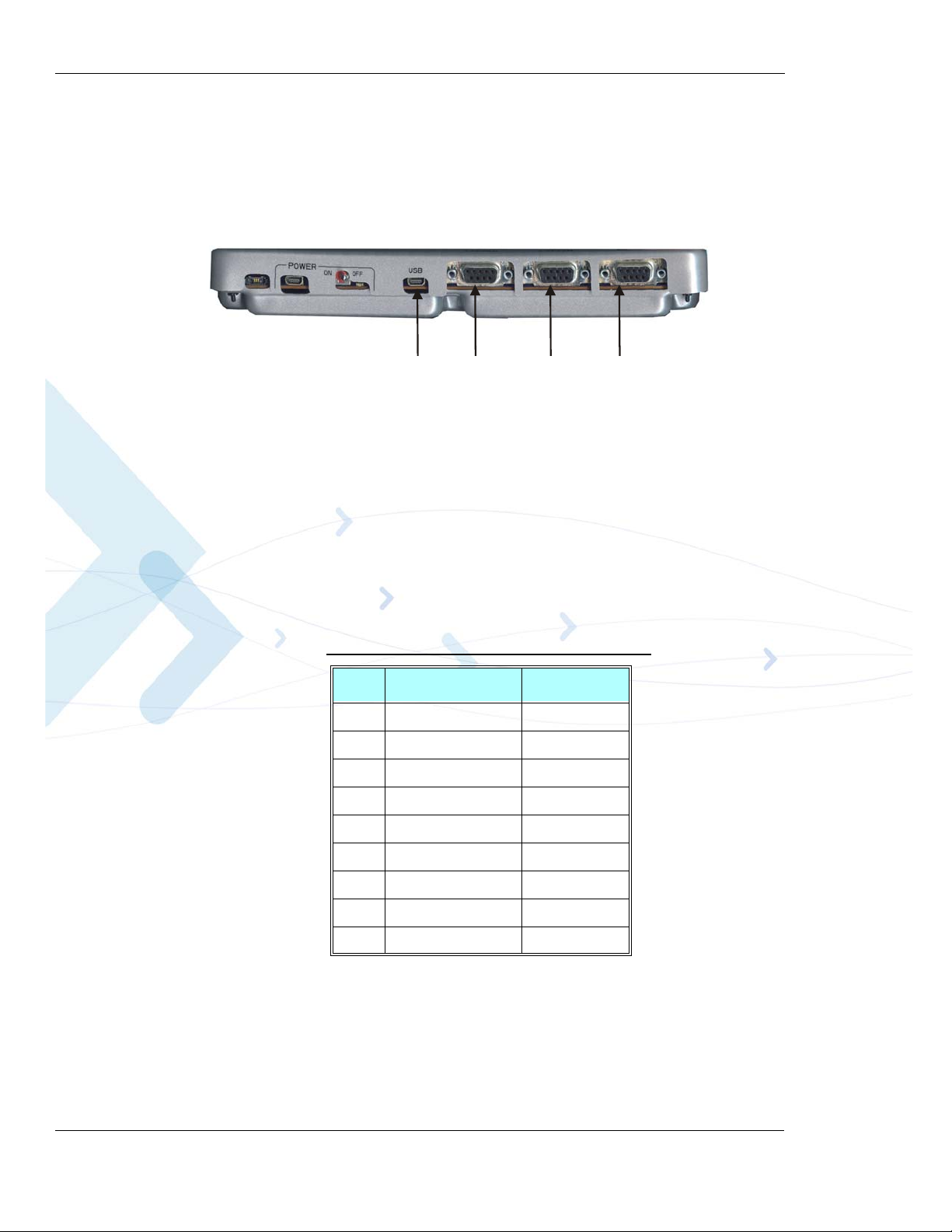
The G30 Developer Board includes four serial interfaces (Figure 2-12):
• Primary RS232-1
Figure 2-12: RS232-1 Connector
This serial interface is described in the sections that follow.
RS232-1
The 9-pin, D-type RS232-1 serial port (J300) is the primary interface to the G30. The G30 UAR T
signals are active-low CMOS-level signals (0-2.7 V), which are converted by the Developer
Board to standard RS232 levels for PC communications. The RS232-1 Connector Pinout (J300)
is shown in Table 2-4.
Note: The RS232-1 connector pin names are DTE-oriented.
Table 2-4: RS232-1 Connector Pinout (J300)
Pin # Description DTE I/O
1 DCD In
2 RXD In
3 TXD Out
4 DTR Out
5 Ground
6 DSR In
7 RTS Out
8 CTS In
9 RI In
RS232-2
The 9-pin, D-type RS232-2 serial port (J330) is used for data logger when G30 adapter is used.
Note: Only the G30 adapter supports Data logger. If G30 with 70 pin connector model is used,
data logger is not applicable.
20 G30 Developer’s Kit December 15, 2009
Page 39
Chapter 2: Developer Board and Interfaces Description
Reset
Button
This UART signals are active-low CMOS-level signals (0-2.7 V), which are converted by the
Developer Board to standard RS232 levels for PC communications. The RS232-2 Connector
Pinout (J3300) is shown in Table 2-5.
Table 2-5: RS232-2 Connector Pinout (J330)
Pin # Description DTE I/O
1 NA NA
2 RXD In
3 TXD Out
4 NA NA
5 Ground
6 NA NA
7 RTS Out
8 CTS In
9 NA NA
On-board Reset Button
Note: The On-Board Reset Button is applicable only when G30 adapter is used.
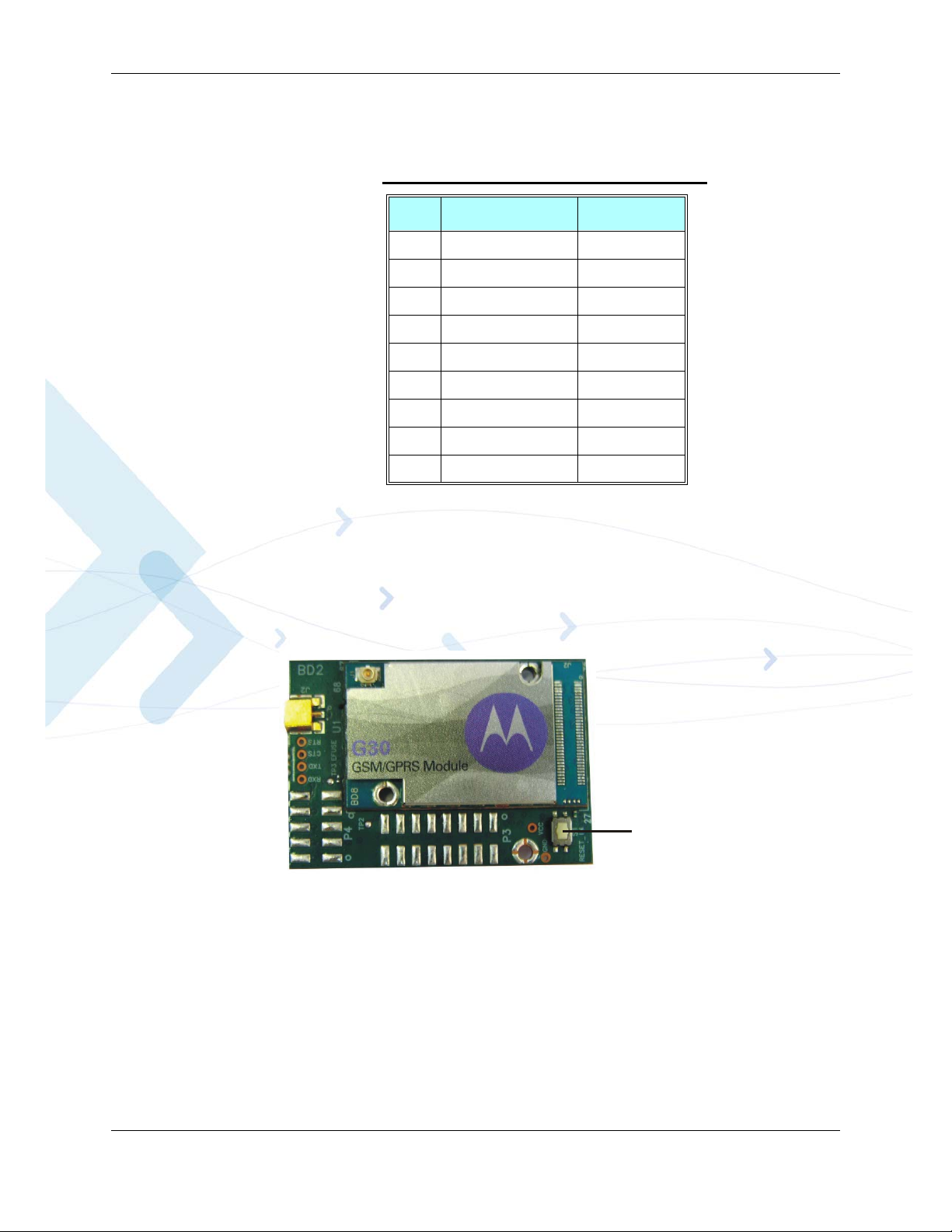
The S1 button is directly connected to G30 reset input pin. Pressing this button causes the module
to perform soft reset. This is valid when the module is turned ON. See Figure 2-13.
Figure 2-13: G30 Reset Switch
December 15, 2009 G30 Developer’s Kit 21
Page 40
Configuration
NA for
G30
Microphone
Connector
Headset
Connector
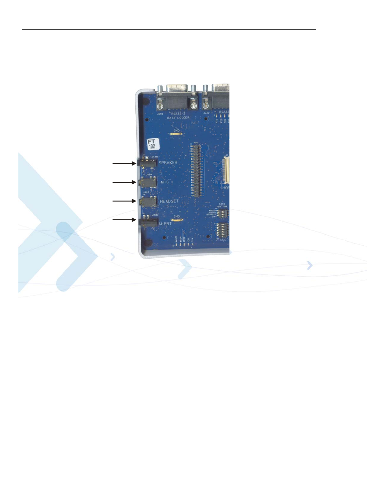
Speaker-Alert
Connector
Audio Interface
The Developer Board includes analog and digital audio interfaces. The audio interface contains a
speaker - alert speaker, microphone, and a headset (Figure 2-14).
Figure 2-14: Audio Connectors
Analog Audio path:
• Handset mode: use "MIC" Input (pin 51), and differential speaker "ALRT_N", "ALRT_P"
outputs (pins 63, 65 of the G30).
• Headset mode:
• When G30 with 70 pin connector is used, "MIC_HDST" Input (pin 57), "HD ST_SPK" output
(pin 54).
• When G30 adapter is used, "MIC_HDST" Input (pin 57), "HDST_SPK" output (pin 67).
Note: In order to operate the G30 EVB with the G30 70 pin connector module, pin 54 of the 70
pin connector, must be manually shorted with pin 67 of the 70 pin connector.
The short can be implemented using 70 pin Header "P100".
22 G30 Developer’s Kit December 15, 2009
Page 41
Chapter 2: Developer Board and Interfaces Description
Alert - Speaker
The Developer Board uses an audio amplifier to amplify the speaker audio output to desired
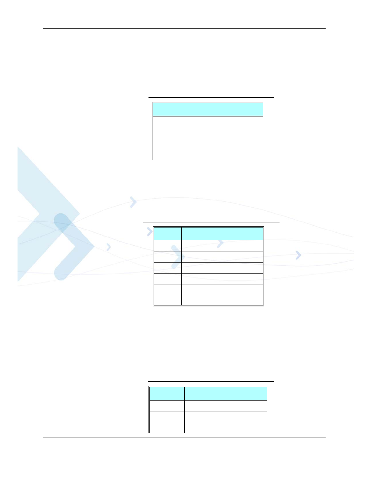
levels. The alert-speaker connector (J480) is labeled ALERT. The speaker output is 8 ohms
impedance. The Speaker Connector pinout (J480) is shown in Table 2-6.
Table 2-6:
Speaker Connector Pinout (J430)
Pin # Description
1 Not connected
2 Speaker positive output
3 Not connected
4 Speaker negative output
Microphone
The microphone connector (J460) is labeled MIC. The Microphone Connector pinout (J460) is
shown in Table 2-7.
Table 2-7: Microphone Connector Pinout (J460)
Pin # Description
1 Ground
2 Not connected
3 Not connected
4 Microphone audio-in
5 Not connected
6 Grounding switch
Headset
The headset interface is designed as a portable phone audio interface, and is similar to a phone
headset interface. The headset connector (J440), labeled HEADSET, includes a speaker,
microphone and a detection signal. The speaker and microphone signals are directly connected to
the G30 audio signals.
The Headset Connector pinout (J440) is shown in Table 2-8.
Table 2-8: Headset Connector Pinout (J440)
Pin # Description
1 Ground
2 Headset-detect switch
3 Speaker audio-out
December 15, 2009 G30 Developer’s Kit 23
Page 42
Configuration
Reference Description "Off" State "On" State
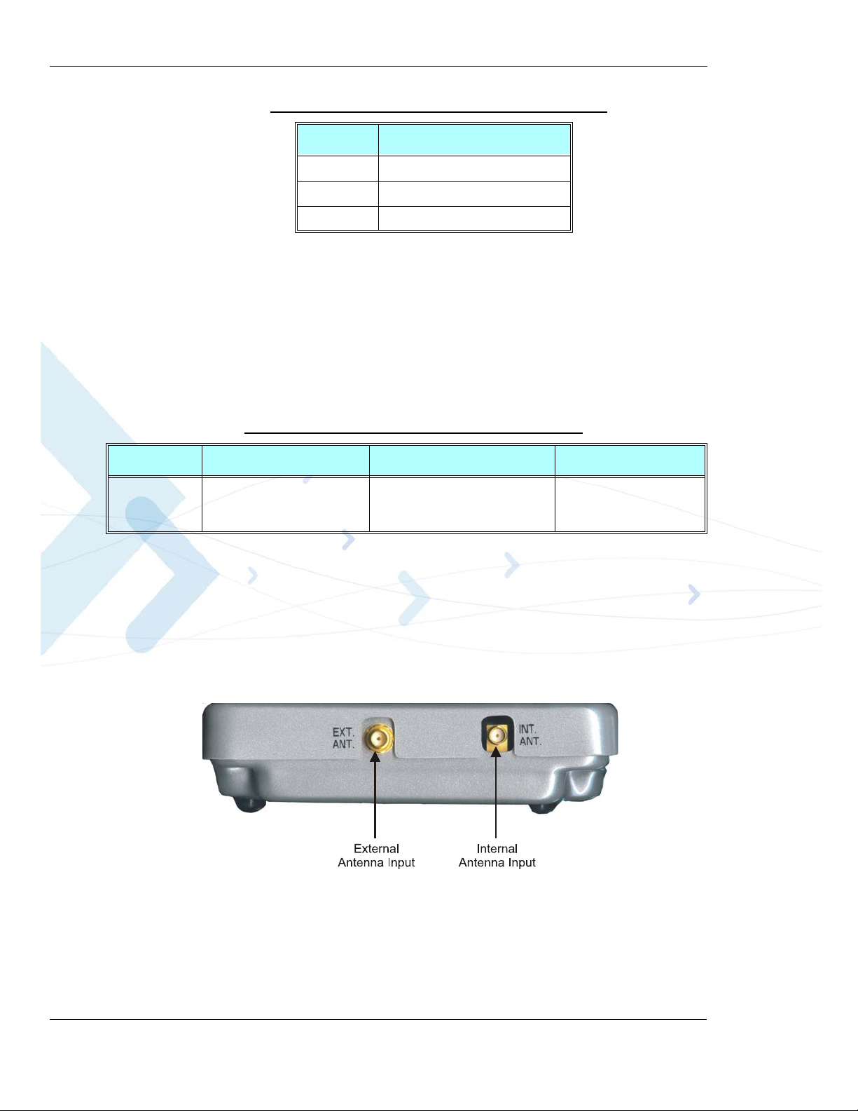
Table 2-8: Headset Connector Pinout (J440) (Cont.)
Pin # Description
4 Microphone audio-in
5 Ground
6 Headset pull down
Audio Source Selection
The microphone and speaker audio can be routed through two different sources, the G30 audio
amplifiers or the G30 digital audio interface. The Developer Board includes an on board CODEC
that converts the G30 digital audio data to analog audio signals.
AUDIO switch of S140 (see Figure 2-21), selects the speaker and microphone so urce, as
indicated in Table 2-9. This enables you to test the digital or analog audio channels.
Table 2-9: Audio Source Selection (S140-"AUDIO")
Audio Selecting between Analog or
Digital Audio.
Antenna
An antenna (internal or external) must be connected to the Developer Board for adequate GSM
reception. You must connect the G30 to either the on-board internal antenna or to an external
antenna.
T wo RF connectors on the right side of the Developer Board, labeled
used for setting up the antenna (Figure 2-15).
Figure 2-15: Antenna Connectors (external)
Analog audio - audio sources are
the G30 audio lines.
Digital audio - audio
source is the on board
CODEC.
INT ANT and EXT ANT , are
On the inside of the Developer Board, the
INT ANT is connected to the on-board internal antenna.
24 G30 Developer’s Kit December 15, 2009
EXT ANT connector is connected to the G30 and the
Page 43
Chapter 2: Developer Board and Interfaces Description
G30 Adapter
RF Cable
G30 Adapter
On-board
Internal
External
RF Cable
EXT ANT
INT ANT
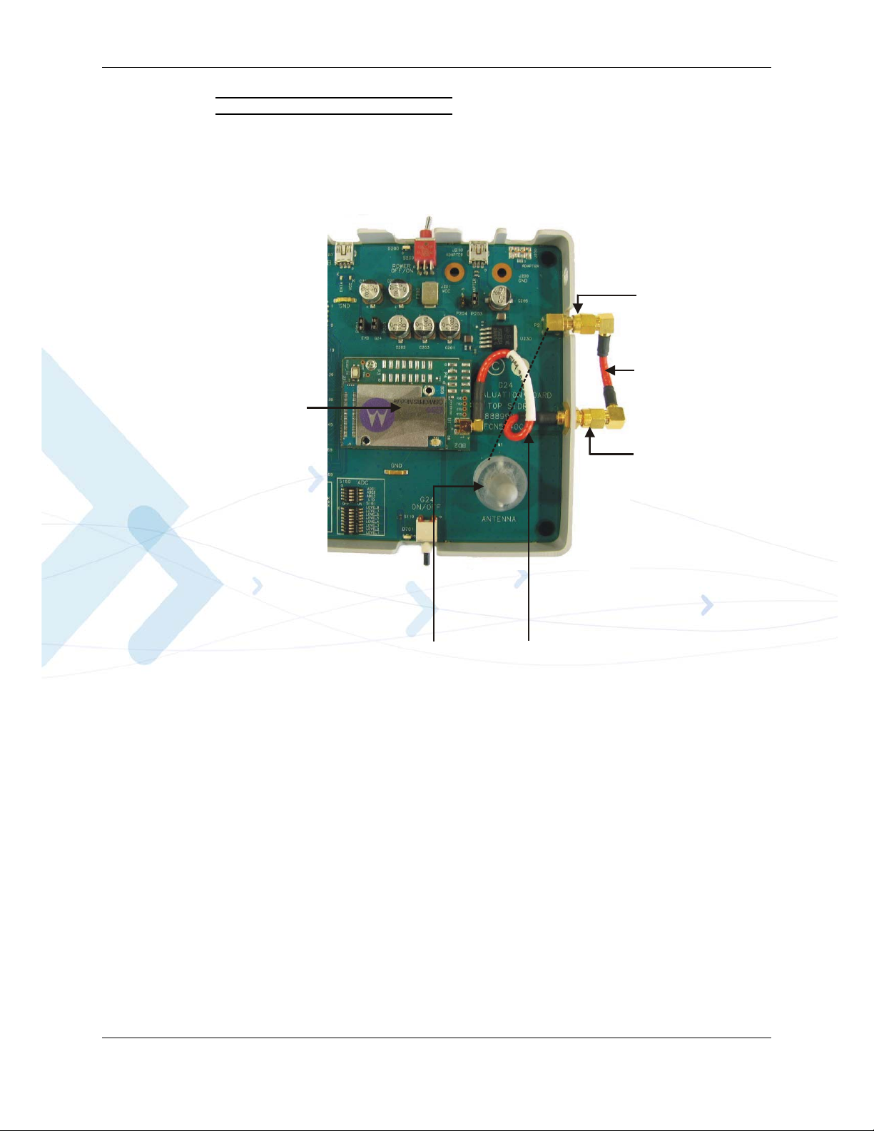
To Connect to the Internal Antenna
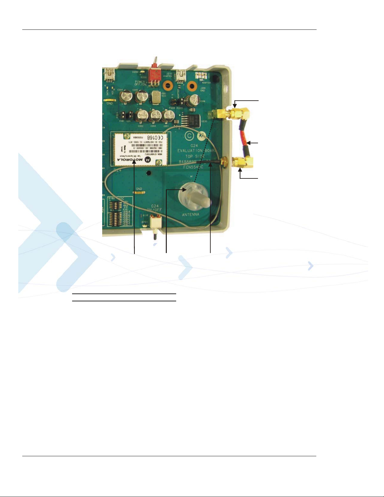
• Connect the EXT ANT and INT ANT connectors with the additional RF cable supplied in the
Developer’s Kit (Figure 2-16 and Figure 2-17).
Note: This is the Developer Board’s default configuration. The board arrives with the EXT ANT
and
INT ANT already connected.
Figure 2-16: Antenna Connectors (internal) - For G30 Adapter
December 15, 2009 G30 Developer’s Kit 25
Page 44
Configuration
G30
RF Cable
G30
On-board
Internal
Antenna
External
RF Cable
EXT ANT
INT ANT
Figure 2-17: Antenna Connectors (internal) - For G30
To Connect to an External Antenna
1. Disconnect the external RF cable from the EXT ANT connector.
2. Connect an external antenna or antenna application to the
and Figure 2-17).
EXT ANT connector (Figure 2-16
The connection cable is not included.
26 G30 Developer’s Kit December 15, 2009
Page 45
Chapter 2: Developer Board and Interfaces Description
S160
S161
Option Switches
The Developer Board contains 7 option switches that are described in the following paragraphs.
Analog to Digital Converter (ADC) - S160, S161
Important: Applying voltage to ADC lines before power up is forbidden and may cause G30
power up issues.
Note: G30 Adapter Board supports dual ADC. ADC1 and ADC2 are applicable.
Note: G30 ADC voltage input range is 0V-1.92V. Therefore, only level 1 to level 7 are
applicable.
The Developer Board can route up to 8 different analog voltage levels to the 3 G30 analog to
digital converters, using the S160 and S161 switches.
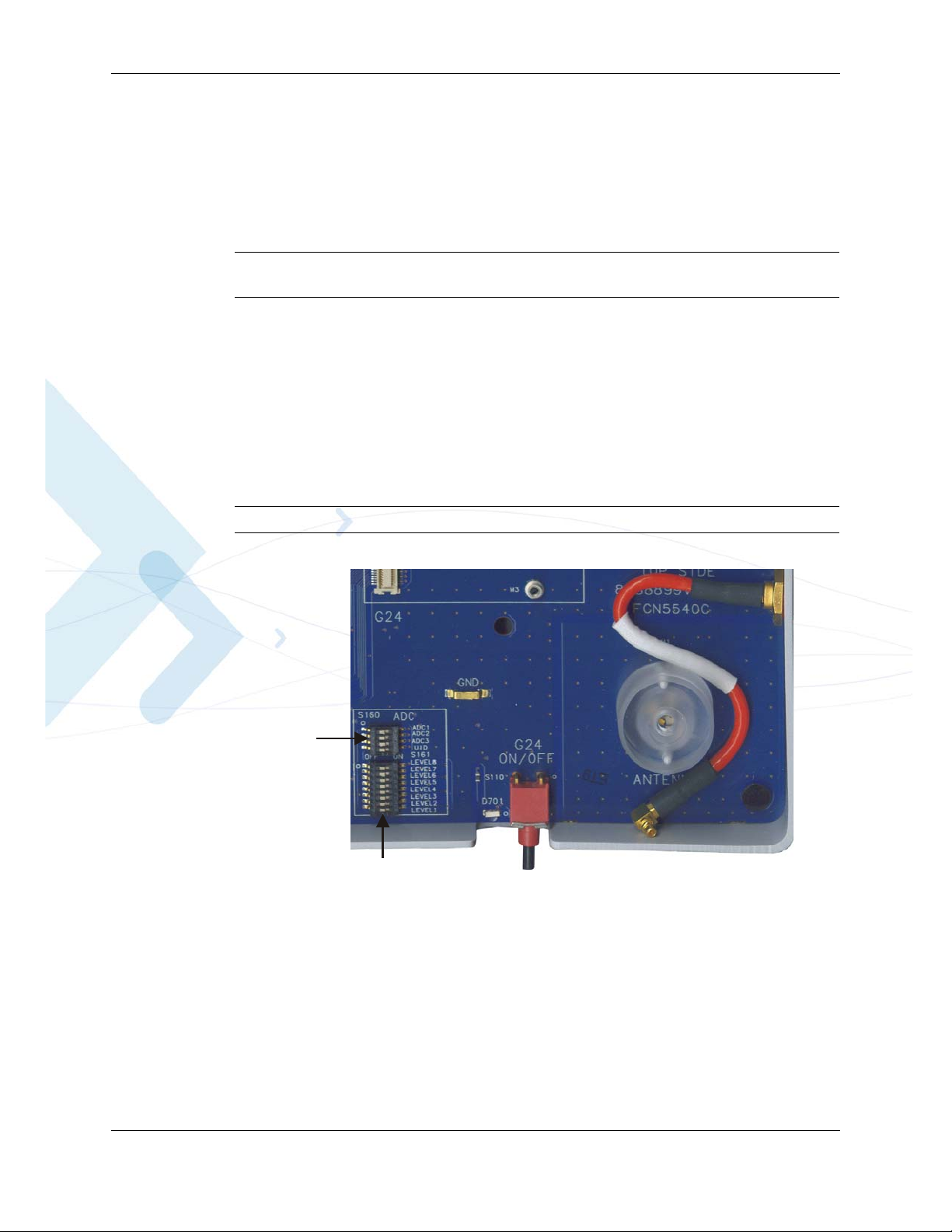
Figure 2-18 shows the ADC switches (S160, S161) provided on the Developer Board, which are
located on the S160, S161 components.
Important: S160 switches must be placed Off (all switches to left side) before power up.
Figure 2-18: S160, S161 Switches
Voltage level is set using the S161 switches and routing of the voltage to the desired A/D is done
using the S160 switched.
When simulating a desired voltage level to either of the A/D lines, perform the following steps:
1. Turn the desired voltage level switch (labeled LEVEL1-LEVEL8) to ON.
Note: In order to have the correct voltage level, verify that only a single level switch is turned
ON.
December 15, 2009 G30 Developer’s Kit 27
Page 46
Configuration
2. Move the desired A/D input switch (labeled ADC1-ADC3) to ON. Selecting more then one
ADC channel is allowed.
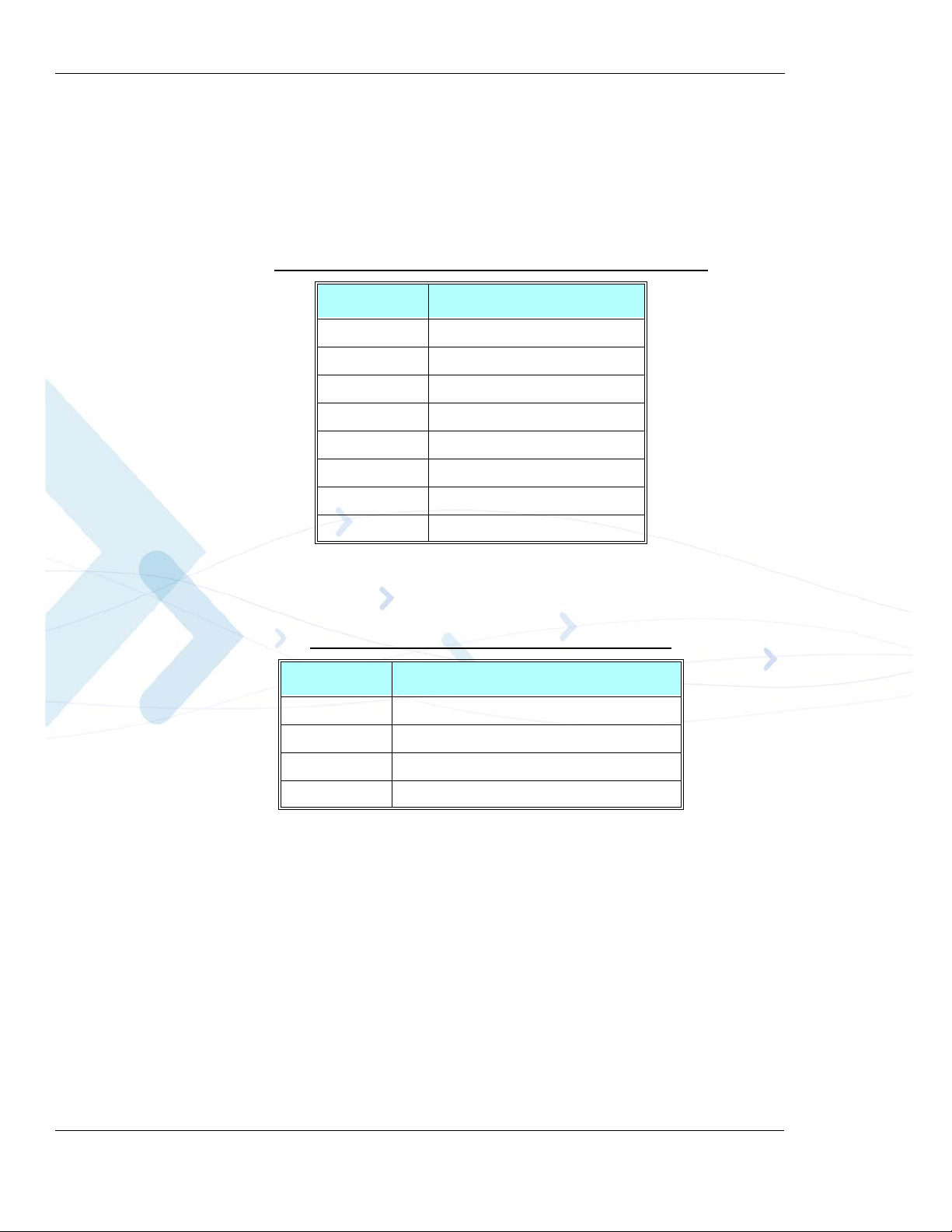
S161 switches are labeled LEVEL1 to LEVEL8 respectively. Voltage levels are shown in
Table 2-10.
Table 2-10:
Voltage Level Settings for A/D Switches (J161)
Reference Analog Voltage Level
LEVEL8 NA
LEVEL7 Setting 1.93V
LEVEL6 Setting 1.59V
LEVEL5 Setting 1.24V
LEVEL4 Setting 0.96V
LEVEL3 Setting 0.68V
LEVEL2 Setting 0.37V
LEVEL1 Setting 0.06V
ADC channel mapping is shown in Table 2-11.
Table 2-11: A/D Selection Switch Settings (J160)
Reference Description
ADC1 Routing voltage level to ADC1 (G30 J1/37)
ADC2 Routing voltage level to ADC2 (G30 J1/43)
ADC3 Do Not Use
N.C Not Used
28 G30 Developer’s Kit December 15, 2009
Page 47
Chapter 2: Developer Board and Interfaces Description
General Purpose I/O (GPIO) - S120
Note: The following GPIOs are G30 GPIO names. In order to verify the G30 GPIOs that are
connected to these pins, refer to “G30 to 70 pin Adapter Board” on page 36.
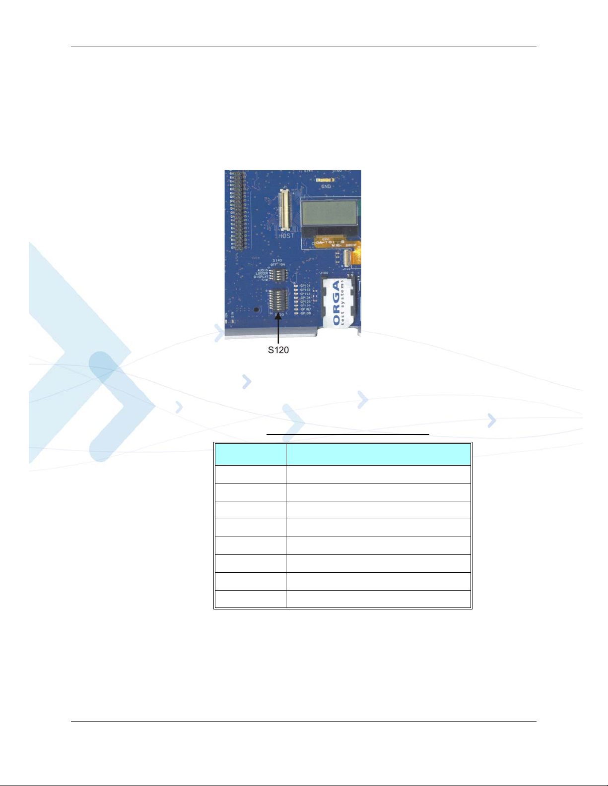
The Developer Board can simulate all 8 G30 GPIO1-GPIO8 states using the S120 switches.
Figure 2-19 shows the GPIO switches provided on the Developer Board, which are located on the
S120 component.
Figure 2-19: S120 Switches
GPIO signals mapping is shown in Table 2-12.
Table 2-12: GPIO Signals Mapping
Reference Description
GPIO1 Map to GPIO1 signal (G30 J1/28)
GPIO2 Map to GPIO2 signal (G30 J1/30)
GPIO3 Map to GPIO3 signal (G30 J1/32)
GPIO4 Map to GPIO4 signal (G30 J1/34)
GPIO5 Map to GPIO5 signal (G30 J1/36)
GPIO6 Map to GPIO6 signal (G30 J1/38)
GPIO7 Map to GPIO7 signal (G30 J1/40)
GPIO8 Map to GPIO8 signal (G30 J1/42)
The G30 GPIO lines can be configured both as output or input lines. The Developer Board
contains 8 LEDs, marked as GPIO1 through GPIO8, that indicate the GPIO state, regardless of its
configuration.
December 15, 2009 G30 Developer’s Kit 29
Page 48
Configuration
The GPIO switches have two positions: Logic High (left position, marked with "H") and Logic
Low (Right position, marked with "L"). When setting a switch to "H" (default position), the
GPIO line is not connected (uses the internal G30 pull-up resistor), when setting the GPIO to "L",
the line is being shorted to ground.
Caution: In order to avoid unnecessary load on one of the GPIO lines, verify that when a
GPIO line is configured as an output and is set to logic High state, the
corresponding GPIO switch is set to "H".
UID - S170
Note: The UID S170 is not applicable for G30 Adapter Board/G30.
Figure 2-20 shows the UID switches provided on the Developer Board, which are located on the
S170 component.
Figure 2-20: S170 Switches
General Function Switch - S140
Note: The S140 is not applicable for G30 Adapter Board/G30.
30 G30 Developer’s Kit December 15, 2009
Page 49
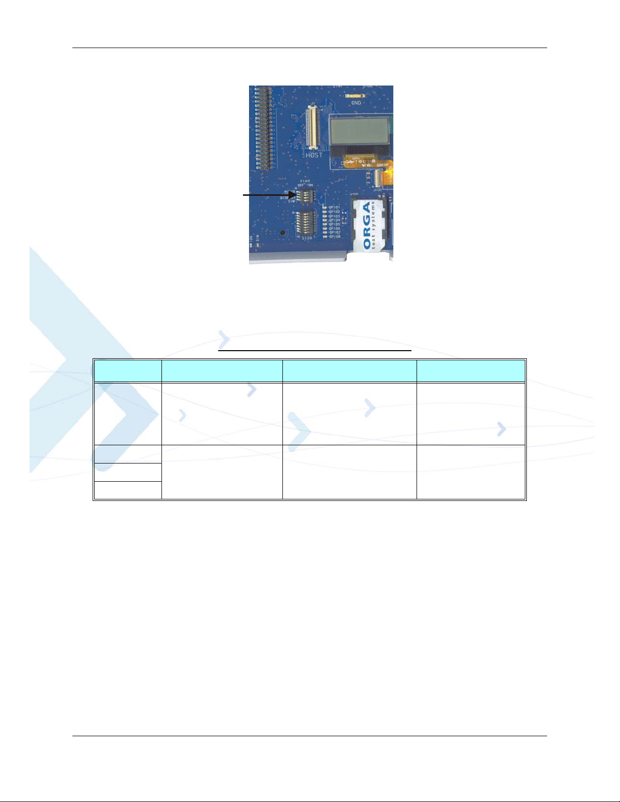
Chapter 2: Developer Board and Interfaces Description
S140
Figure 2-21 shows the S140 switches.
Figure 2-21: S140 Switches
The S140 switches description and functionality are shown in Table 2-13.
Table 2-13: S140 Switches Functionality
Reference Description "Off" State "On" State
AUDIO Selecting the audio speaker
output path.
LOGGER Used for development only.
DISPLAY
SIM
Verify that the switch is
always at "OFF".
Disabling the on board audio
CODEC to Audio speaker.
Speaker and microphone analog
audio are routed from the G30
module.
Switch should always be at this
state.
Enabling the on board
audio CODEC to Audio
speaker. Au dio is routed
using the G30 digital audio
signals.
General Function Switch - S141
Note: The S141 is not applicable for G30 Adapter Board/G30.
The S141 switches are used for development purpose only and should remain at OFF (left
position) for proper use of the G30.
December 15, 2009 G30 Developer’s Kit 31
Page 50
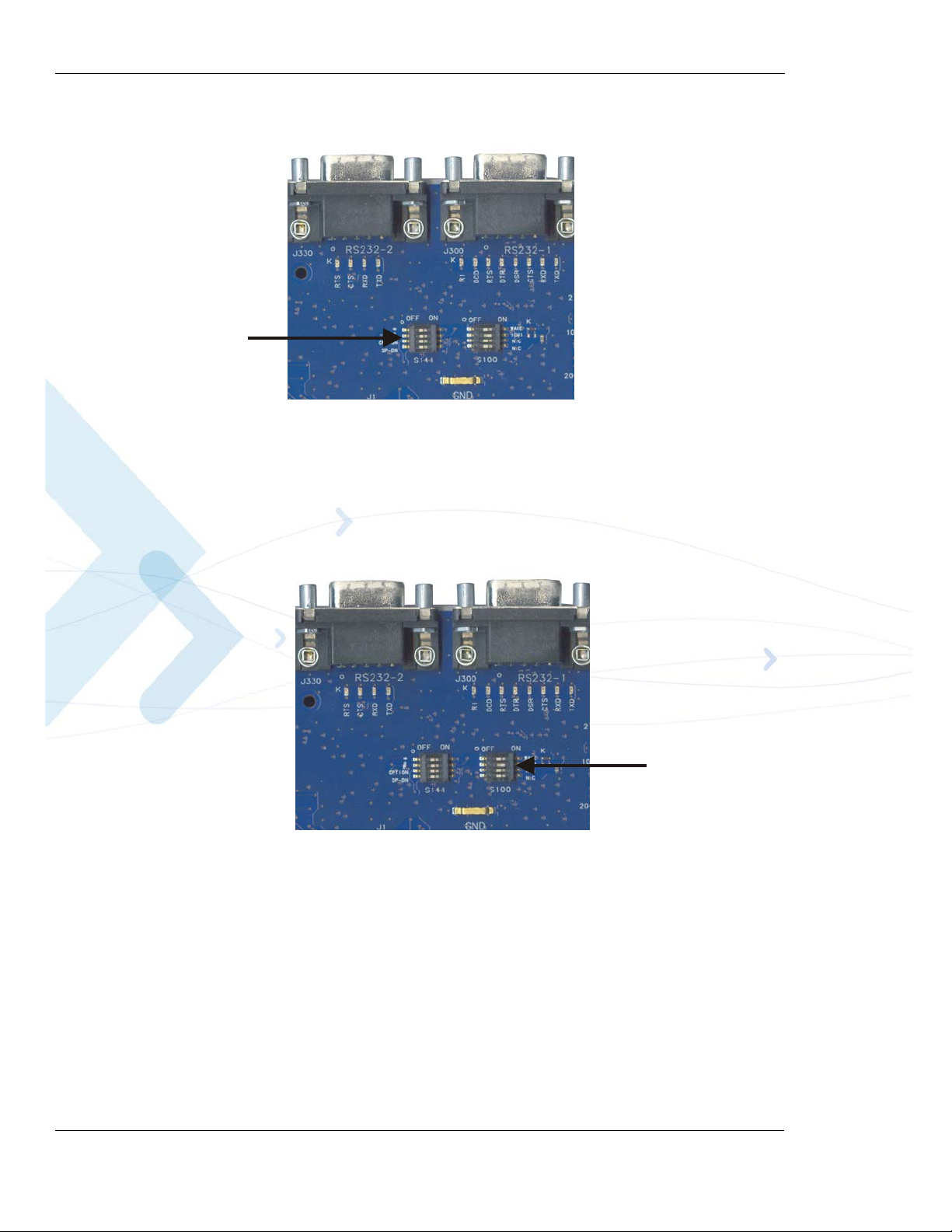
Configuration
S141
S100
Figure 2-22 shows the S141 switches.
Figure 2-22: S141 Switches
General Function Switch - S100
Note: The S100 is not applicable for G30 Adapter Board.
Figure 2-23 shows the S100 switches.
Figure 2-23: S100 Switches
32 G30 Developer’s Kit December 15, 2009
Page 51
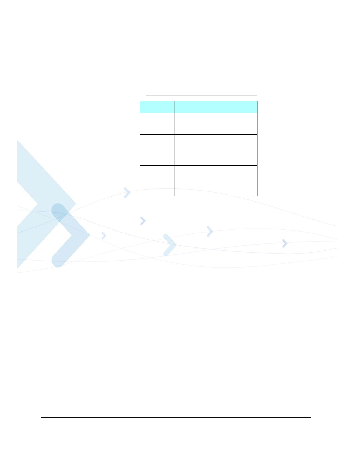
Chapter 2: Developer Board and Interfaces Description
SIM Card
The SIM card connector (J100) is external to the G30, but is connected directly to it, similar to an
internal SIM. The G30 can accept 3V SIM cards. The SIM Connector pinout (J100) is shown in
Table 2-14.
Table 2-14:
SIM Connector Pinout (J100)
Pin Description
1 Ground
2 Presence detect
3 Clock
4 Reset
5 VCC
6 Serial data I/O
7 VPP (not connected)
8 Ground
G30 detects the presence of the SIM card through the SIM_PD signal. This signal is configured in
the G30 as Active-Low.
December 15, 2009 G30 Developer’s Kit 33
Page 52
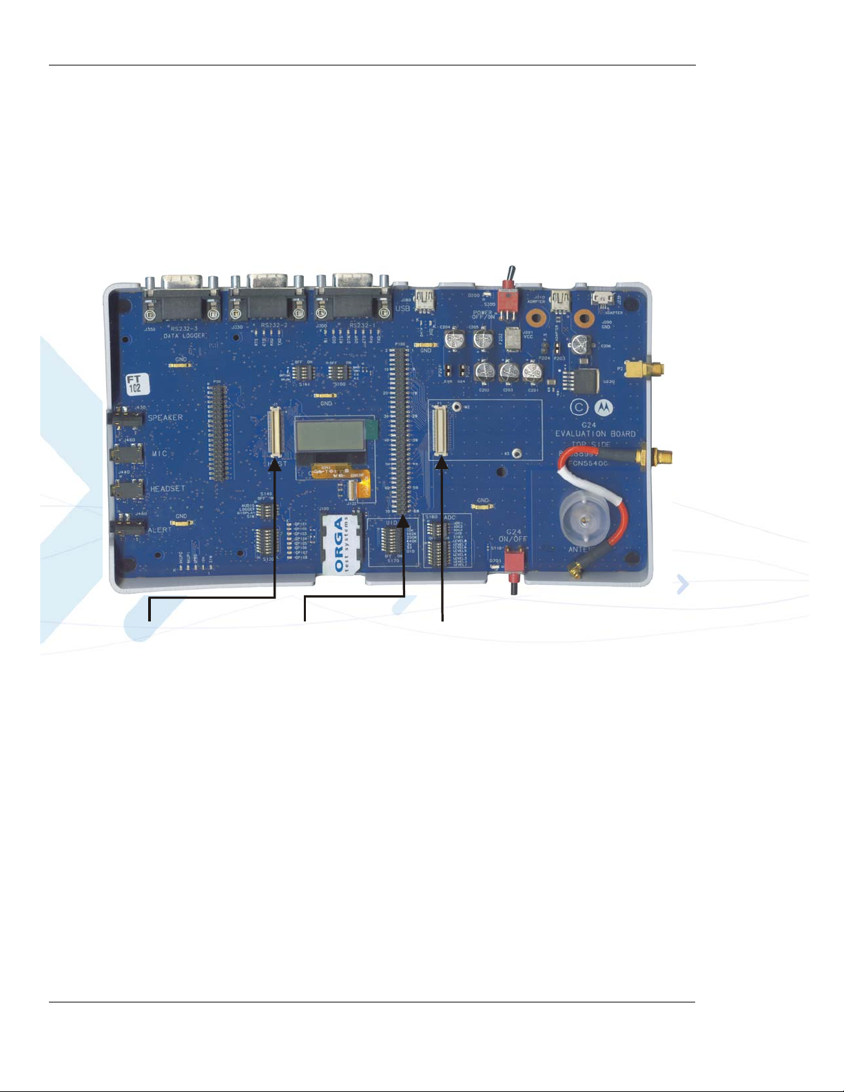
Configuration
G30/G30 Adapter
70-pin Connector
G30 70-pin
Header Connector
70-pin
Host Connector
Host Connection
An external application may communicate with the G30 through the host connector (J1)
(Figure 2-24) and control some or all of the G30's functions. The host connector enables yo u to
integrate the G30 into an application without installing the G30 inside the product.
The host connector operates in parallel with the Developer Board peripherals and enables an
external application to share G30 resources with the Developer Board. You may select any G30
function to control externally, through the host connector, and allow the Developer Board to
control other functions.
Figure 2-24: 70-pin Connectors
34 G30 Developer’s Kit December 15, 2009
You can connect an external application to the G30 Developer Board using a host interconnect
flex cable and connecting it to the host connector (J1). Connect the other end of the cable to the
external application. The cable is an optional accessory.
All pin numbers and functions of the host connector are identical to those of the G30 (P1) and the
G30 diagnostic connector (P100). For more information on the pins of the host connector, refer to
“G30 to 70 pin Adapter Board” on page 36.
These are guidelines for using the host connector:
• When using an external SIM card through the host connector, the Developer Board SIM card
tray must be empty
• When using any of the serial communication channels (RS232, LOGGER) through the host
connector, the Developer Board serial connectors should not be used
• When using the WAKEUP functions through the host connector, the functions should be
switched off on the Developer Board switches
• When using the analog audio channels through the host connector, disconnect all audio
devices from the Developer Board
Page 53

Chapter 2: Developer Board and Interfaces Description
• It is recommended to place the audio selection switch (S140 - AUDIO) to analog audio mode
(OFF)
• When connecting an external application that provides the power to the G30 and the
Developer Board, remove any other power sources from the Developer Board
December 15, 2009 G30 Developer’s Kit 35
Page 54
Components and Specifications
Components and Specifications
Connectors Description
All the Developer Board connectors are marked by their reference number and by a pin-1
indicator. Table 2-15 describes the available connectors on the Developer Board.
Table 2-15: Developer Board Connectors
Reference Connector Description
Internal Connectors (not visible when cover is on)
P1 G30 UUT G30 UUT (Unit Under Test) connector
J1 Host Emulates the G30 connector for host systems
P100 Header Debug header connector (70-pin)
P50 Header For development use only
J201 VCC Developer Board DC power supply
J200 GND Developer Board common ground
External Connectors (visible when cover is on)
J380 USB USB mini AB-type connector, applicable for
J300 RS232-1 Primary RS232 to PC
J330 NA
J350 NA
J430 Speaker Hands-free system speaker jack
J460 Microphone Hands-free system microphone jack
J440 Headset Headset jack
J480 NA
J210 AC adapter/char ger Wall-mount adapter connector
J100 SIM card SIM card socket with detection
P2 Antenna connector SMA connector for internal antenna
M1 RF Antenna Internal antenna
G30 to 70 pin Adapter Board
G30 Adapter Board with charger model
The following table lists the pin names and functions available for the G30 to 70 pin interface
connector. All pin numbers and functions are identical to the G30 (P1), host (J1) and G30 Diagnostic (P100) connectors on the Developer Board.
36 G30 Developer’s Kit December 15, 2009
Page 55
Chapter 2: Developer Board and Interfaces Description
@70 Pin
Conn.
36 1 GPIO5 I/O GPIO
38 2 GPIO6 I/O GPIO
56 4 eSIM_RESET I Embedded SIM reset
40 5 GPIO7 I/O GPIO
42 6 GPIO8 I/O GPIO
62 7 SPI_IRQ
41 13 ANT_DET
26 14 WKUPO
49 16 GPRS
Pin No. Name I/O Function
I SPI Interrupt Input
I/O Capture/Compare
I/O GPIO
12 GPIO9 I/O GPIO
I/O GPIO
O Antenna Detect
I/O GPIO
O Wake-Up Out
I/O GPIO
OGPRS
53 18 PWR_ON I Power-on/off input
48 20 VSIM O SIM supply output
44 21 SIM_RST O External SIM reset
52 22 SIM_IO I/O SIM data
46 23 SIM_CLK O SIM clock
16 25 WKUPI
25 27 RESET_IN OC External reset input
34 33 GPIO4/SCL
I/O Capture/Compare
I Wake-Up In
2
O
I/O GPIO
C bus clock line
I
December 15, 2009 G30 Developer’s Kit 37
Page 56
Components and Specifications
@70 Pin
Conn.
32 34 GPIO3/SDA
43 35 ADC2 I
37 36 ADC1 I
23 37 RI
17 38 DCD O Data Carrier Detect
13 39 DSR O Data Set Ready
19 40 DTR I Data terminal ready
941RTS I Ready to send
15 42 CTS O Clear To Send
Pin No. Name I/O Function
2
I/O
I
C bus data line
I/O GPIO
Analog-to-Digital
Converter Input
Analog-to-Digital
Converter Input
O Ring Indicator
I/O GPIO
21 43 TXD I
11 44 RXD O
66 45 SPI_CLK O
54 47 HDST_SPK O
63,67 48 SPKR_N O
65,69 49 SPKR_P O
55 50 HDST_INT
61 51 MIC I
59 52 AGND1 I
57 53 MIC_HDST I
Transmitted Data
GPIO
Received Data
GPIO
SPI Clock
Short to Pin 57
Low power single-ended
analog audio output
High power differential
analog audio output
High power differential
analog audio output
Headset detection
I
input
External interrupt
I
input
I/O GPIO
Headset microphone
analog bias
Handset microphone
analog reference
Headset microphone
analog bias
38 G30 Developer’s Kit December 15, 2009
Page 57
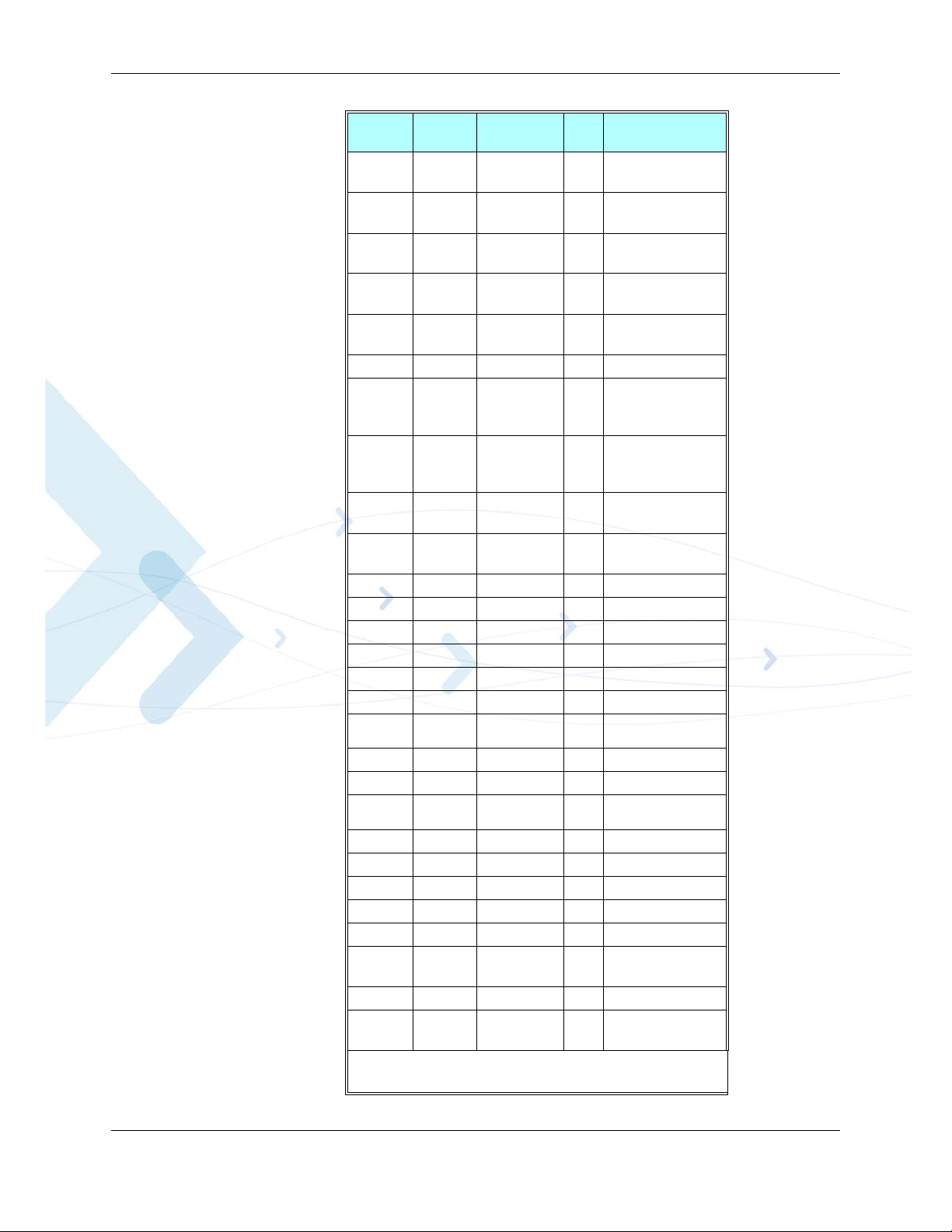
Chapter 2: Developer Board and Interfaces Description
@70 Pin
Conn.
59 54 AGND2 I
18 55 RXD_DAI I
24 56 WA0_DAI O
22 57 CLK_DAI O
20 58 TXD_DAI O
50 59 SIM_PD_n I SIM present detect
68 60 SPI_MOSI O
64 61 SPI_MISO I
60 62 VRTC I/0
70 63 SPI_CS O
1,2,3,4 65 GND NA Ground
N.C
1,2,3,4 67 GND NA Ground
1,2,3,4 68 GND NA Ground
1,2,3,4 69 GND NA Ground
1,2,3,4 70 GND NA Ground
Pin No. Name I/O Function
Headset microphone
analog reference
I2S receive data
Short to pin 61
I2S word alignment
Short to pin 60
I2S clock
Short to pin 45
I2S transmit data
Short to pin 63
SPI sync data
(MOSI)
Shorted to pin 56
SPI sync data
(MISO)
Shorted to pin 55
Real Time Clock
Supply Output
SPI chip select
Short to pin 58
66 ANT I/O RF antenna
1,2,3,4 71 GND NA Ground
1,2,3,4 72 GND NA Ground
1,2,3,4 73 GND NA Ground
1,2,3,4 74 GND NA Ground
1,2,3,4 75 GND NA Ground
1,2,3,4 76 GND NA Ground
1,2,3,4 77 GND NA Ground
5,6,7,8 78 VCC I Voltage Supply Input
5,6,7,8 79 VCC I Voltage Supply Input
28 80 GPIO1 I/O GPIO
30 81 GPIO2 I/O GPIO
27 VREF O
Not Connected – Refer to "RF Recommendation in G30
Module Description Manual".
December 15, 2009 G30 Developer’s Kit 39
Reference voltage
supply
Page 58
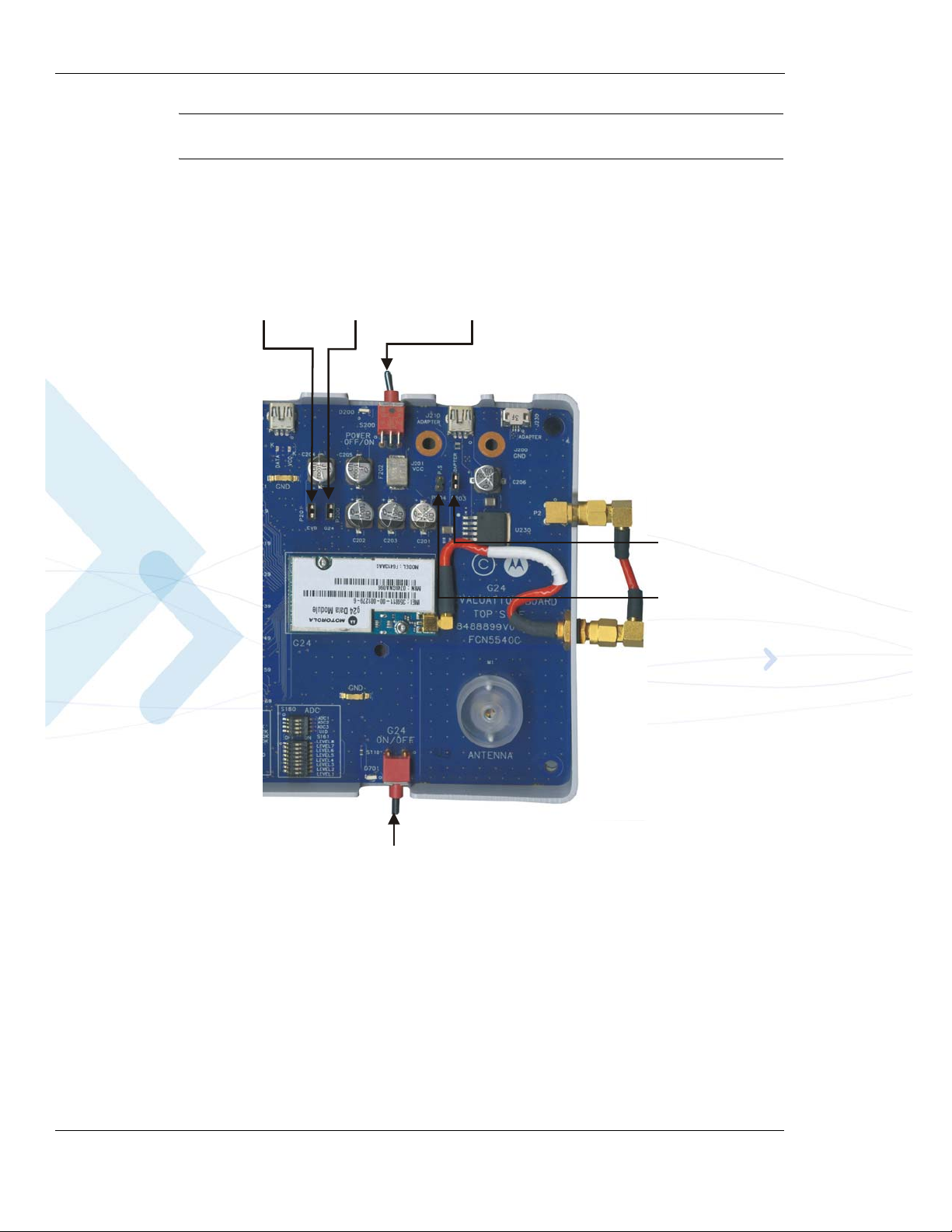
Components and Specifications
P200
(G30 Power
Jumper)
S200
(Power On/Off
Switch)
S110
(G30 On/Off
Pushbutton)
P203
(Adapter Power
Jumper)
P204
(P.S Power
Jumper)
P201
(Developer Board
Power Jumper)
Important: Applying voltage to ADC lines before power up is forbidden and may cause G30
Switches and Jumpers
Figure 2-25 shows the jumpers and switches on the Developer Board.
power up issues.
Figure 2-25: Jumpers and Switches on Developer Board
40 G30 Developer’s Kit December 15, 2009
Page 59
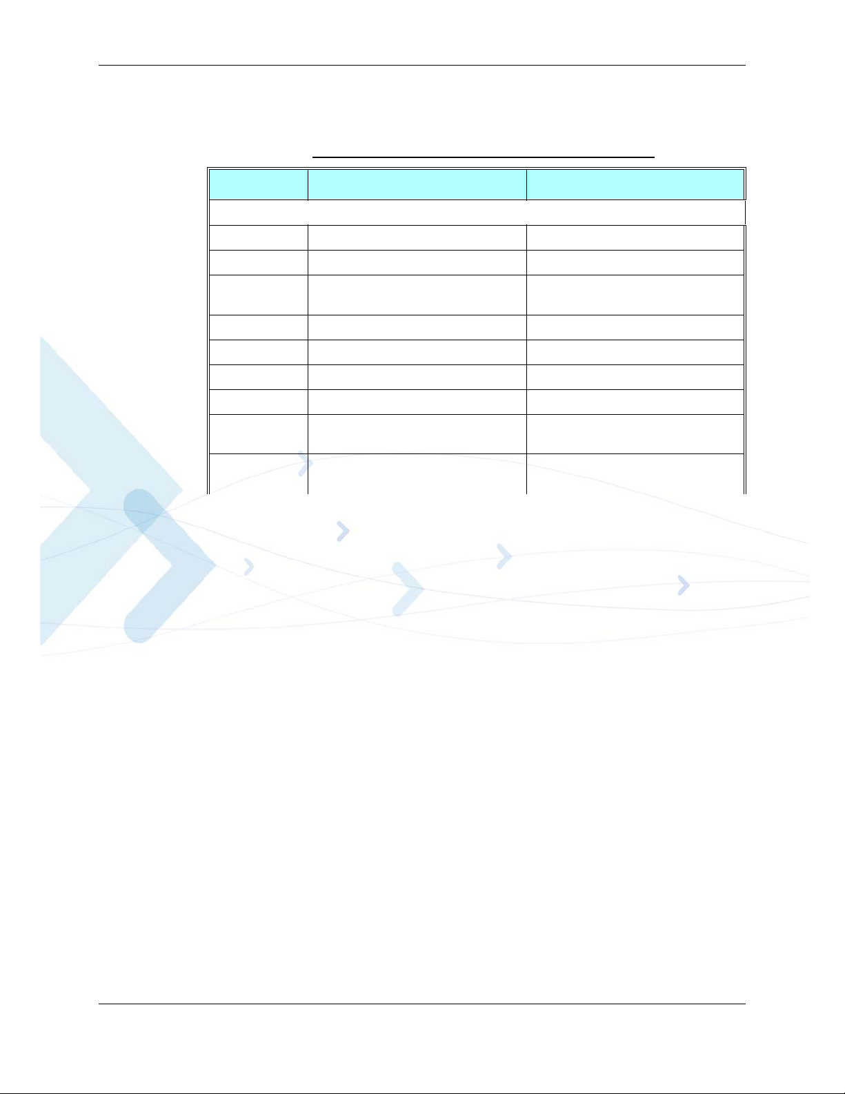
Chapter 2: Developer Board and Interfaces Description
Table 2-16 describes the available switches and jumpers on the Developer Board.
Table 2-16:
Developer Board Switches and Jumpers
Reference Switch/Jumper Description
Switches
S200 Board on/off Developer Board on/off switch
S110 G30 on/off G30 on/off pushbutton switch
S100 General Function Switch Four switches for Developer Board
options
S141 NA
S140 NA
S120 GPIO Switch Eight switches for GPIO signals
S170 UID Switch Eight switches for development use only
S160 ADC Switch Eight switches for simulating ADC sig-
nals
S161 ADC Switch Eight switches for simulating ADC sig-
nals
December 15, 2009 G30 Developer’s Kit 41
Page 60
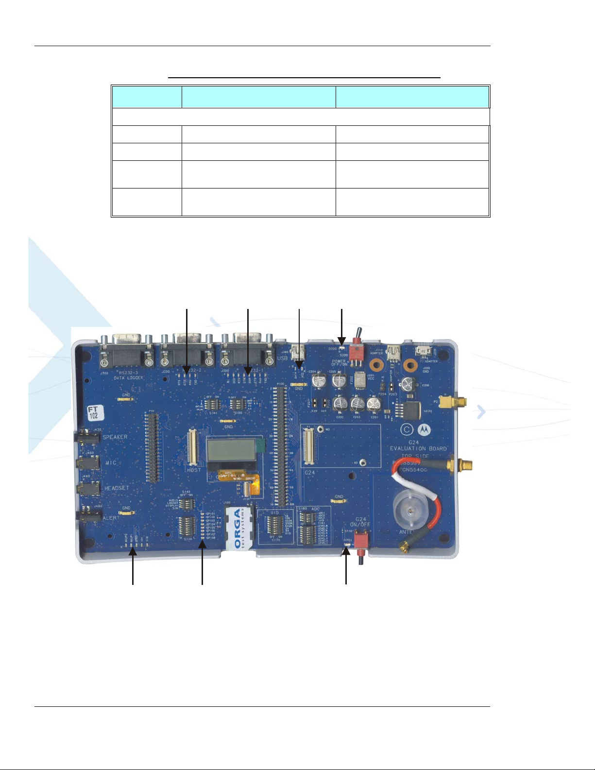
Components and Specifications
Developer
Board Power
G30
On/Off
GPIO
LEDs
General
LEDs
USB
LEDs
RS232-1
LEDs
RS232-2
LEDs
Reference Switch/Jumper Description
Jumpers
P201 EVB Peripheral power input jumper
P200 UUT G30 UUT power input jumper
P203 ADAPTER Wall mount adapter power source selec-
P204 P.S External power supply, power source
LED Indicators
Figure 2-26 shows the LEDs on the Developer Board.
Table 2-16: Developer Board Switches and Jumpers (Cont.)
tion jumper
selection jumper
Figure 2-26: LEDs on Developer Board
Note: Some LED indicators detailed in the table below are not applicable for G30 Adapter
Board.
42 G30 Developer’s Kit December 15, 2009
Page 61
Chapter 2: Developer Board and Interfaces Description
Table 2-17 describes the LED indicators on the Developer Board. Each LED is marked on the
board by the function it represents.
Table 2-17:
Developer Board LED Indicators
Group LED Reference Description
General WAKEUPO D768 Wake-up out
WAKEUPI D704 Wake-up in
IGN D 702 Ignition input
GPRS D710 GPRS/EGPRS coverage indi-
cation
SIM D707 SIM card reset indication
GPIO GPIO1 D760 General purpose I/O 1 signal
GPIO2 D761 General purpose I/O 2 signal
GPIO3 D762 General purpose I/O 3 signal
GPIO4 D763 General purpose I/O 4 signal
GPIO5 D764 General purpose I/O 5 signal
GPIO6 D765 General purpose I/O 6 signal
GPIO7 D766 General purpose I/O 7 signal
GPIO8 D767 General purpose I/O 8 signal
Power G30 D701 G30 on/off
Power D200 Developer Board Power
USB VCC D780 USB VBUS
DATA D711 USB D+
RS232-1 RXD D722 DTE receive data
TXD D721 DTE transmit data
RTS D724 Request to send
CTS D723 Clear to send
DTR D725 Data terminal ready
DSR D726 Data set ready
DCD D727 Carrier detect
RI D728 Ring indicator
RS232-2 RXD D743 DTE receive data
TXD D742 DTE transmit data
CTS D744 Clear to send
RTS D745 Request to send
December 15, 2009 G30 Developer’s Kit 43
Page 62

Components and Specifications
This page intentionally left blank.
44 G30 Developer’s Kit December 15, 2009
Page 63

Chapter 3: Service and Troubleshooting
Service
This section provides contact information for any possible queries that may arise, for example:
• Have questions?
• Having trouble getting the Developer Board set up?
• Technical questions?
• Configuration questions/problems?
• Technical operating problems?
• Need documentation?
Who to Contact?
The Customer Care Group is ready to assist you on integration issues.
Direct Customer
Use this following email address to contact customer assistance:
Note:
The support services provided by Motorola are subject to the agreement between the
customer and Motorola and may be at an additional charge to the customer . Motorola will
inform the customer in advance of any such charge.
Indirect Customer
Please contact your Motorola licensed distributor.
December 15, 2009 G30 Developer’s Kit 45
Page 64
Troubleshooting
Troubleshooting
Table 3-1 lists problems that may occur during board operation, and describes how to resolve
them. If the problem persists, please contact your Motorola representative.
Problem Indication Action
Power
Table 3-1: Troubleshooting
Developer board does not
power up
The G30 does not
power up or does not
communicate
High current
consumption
GSM Reception
No GSM reception
available
Power LED does not light Check the power source connection.
If using an external DC power source, verify that the
supply is within the limits of 3.3 V to 4.2 V.
Verify that the board power switch (S200) is on.
Check the source jumper (P203 or P204) position.
Verify that the EVB jumper (P201) is present.
The G30 on/off LED doesn’t light or
lights for a short period
The G30 on/off LED lights up automatically when power is applied
The G30 on/off LED blinks
The resetable fuse is turned on Check the polarity of the DC power inputs.
The G30 unit searches unsuccessfully
for network
Check the G30 connection to the Developer Board.
Verify that the UUT jumper (P203 or P204) is present.
Depress the G30 on/off pushbutton for a longer period.
Contact your Motorola representative.
Verify that only one optional power source is connected.
If using an external DC power source, verify that the
supply is within the limits of 3.3 V to 4.2 V.
Fasten the G30 to the board with the supplied screws.
Check the MMCX RF cable connection to the G30.
Fasten the RF cable connections between the EXT
ANT and INT ANT connectors.
Fasten the onboard antenna stub into its base.
SIM card
The SIM card does
not operate
Serial Communications
The RS232 port does not
work with the PC
Audio
The headset does
not work
46 G30 Developer’s Kit December 15, 2009
The SIM LED does not illuminate Verify that the SIM card operates at 3 V.
Verify that the SIM card is inserted properly into its
tray.
The PC does not communicate Check the serial cable connection to the PC.
Verify that the PC port settings comply with the G30
defaults.
Incorrect RS232 LEDs are lit Contact your Motorola representative.
No sound in the headset earpiece or
No sound is produced from the headset microphone
Verify that the headset is inserted correctly into the
headset (J440) audio connector.
Use only the supplied headset.
Check the G30 volume level.
Page 65
Acronyms and Abbreviations
ACD
E
GIL
M
Abbreviation Full Name
A ADC
C CMOS
C CODEC
D DIAG
D DTE
E EGPRS
E EME
E ESD
E EVB
G GPRS
G GSM
Analog to Digital Converter
Complementary Metal Oxide Semiconductor
Coder-Decoder
Diagnostics
Data Terminal Equipment (such as terminals, PCs and so on)
Enhanced General Packet Radio Service
Electromagnetic Emission
Electro-Static Discharge
Evaluation Board
General Packet Radio Service
Global System for Mobile Communications
I IRQ
L LED
M MIDI
M MMCX
M MMI
December 15, 2009 G30 Developer’s Kit Acr & Abbr-1
Interrupt Request
Light Emitting Diode
Musical Instrument Digital Interface
Mini Micro Coax
Man-Machine Interface
Page 66
Abbreviation Full Name
O
P
R
S
U
O OEM
P PCM
R RF
S SIM
S SPI
U UART
U USB
U UUT
Original Equipment Manufacturer
Pulse Code Modulation
Radio Frequency
Subscriber Identity Module
Serial Peripheral Interface
Universal Asynchronous Receiver Transmitter
Universal Serial Bus
Unit Under Test
Acr & Abbr-2 G30 Developer’s Kit December 15, 2009
Page 67

Index
Numerics
70-pin Connectors, 7, 9–10
A
AC Adapter
Connector Pins, 17
Voltage, 17
Accessories, 3
Alert Transducer, 7, 22
Antenna, vi, 9–10, 14
External, 24
Internal, 25
Audio, 13, 22, 24
Amplifier, 23
Analog, 24
Digital, 24
Headset, 13, 22–23
Microphone, 13, 22
Speaker, 13, 22
C
Communications, 12, 20
D
Developer Board
Board Number
ESD, vi
Diagnostics
Connector
Dip Switches, 27
, 3
, 34
E
External DC Power, 12, 16, 18
External Power Source
Jumpers, 18
G
G30
Connecting to Antenna
Header Connection, 34
GND, 18
GSM
Reception
, 24
, 9–10
H
Header Connection, 7
Header Connector, 36
Headset, 13, 22–23
Connector Pins, 23
Host Connector, 34
Flex Cable, 34
J
Jumpers, 7, 40
Audio, 24
Power Source, 16, 35
L
LEDs, 7, 14–15, 42
M
Microphone, 13, 22
Connector Pins, 23
MMCX Connector, 9
O
OEM, v
P
Parts List, 3
Power Jumpers, 16
Power Supply, 7
AC Adapter, 12, 16
Battery, 12
Developer Board Power Jumper, 19
External DC Power, 12, 18
Jumpers, 16, 19, 35
Power Jumper, 19
VCC, 18
Voltage, 18
Power Switch, 12
R
RF Cable, 9, 14, 25
RS232, 20
Connector Pins, 20
S
SIM Card, 7, 33
Connector Pins, 33
Voltage, 33
Spacers, 9–10
Speaker, 13, 22
Switches, 7, 40
U
USB, 12
UUT , 34
V
Voltage
AC Adapter, 17
December 15, 2009 G30 Developer’s Kit Index-1
Page 68

Index V - V
Index-2 G30 Developer’s Kit December 15, 2009
Page 69

Page 70

@6802986C48@
6802986C48-A
MOTOROLA and the Stylized M Logo are registered in the US Patent & Trademark Office.
All other product or service names are the property of their respective owners.
©Copyright 2005 Motorola, Inc.
Java™T echnolo gy and/ or J2ME™: Java and all o ther Java– based ma rks are trad emarks or re gistered
trademarks of Sun Microsystems, Inc. in the U.S. and other countries.
UNIX® : UNIX is a registered trademark of The Open Group in the United States and other countries.
 Loading...