

Motorola DTC114YE Datasheet
SEMICONDUCTOR TECHNICAL DATA
Order this document
by DTC114YE/D
NPN Silicon Surface Mount Transistor with
Monolithic Bias Resistor Network
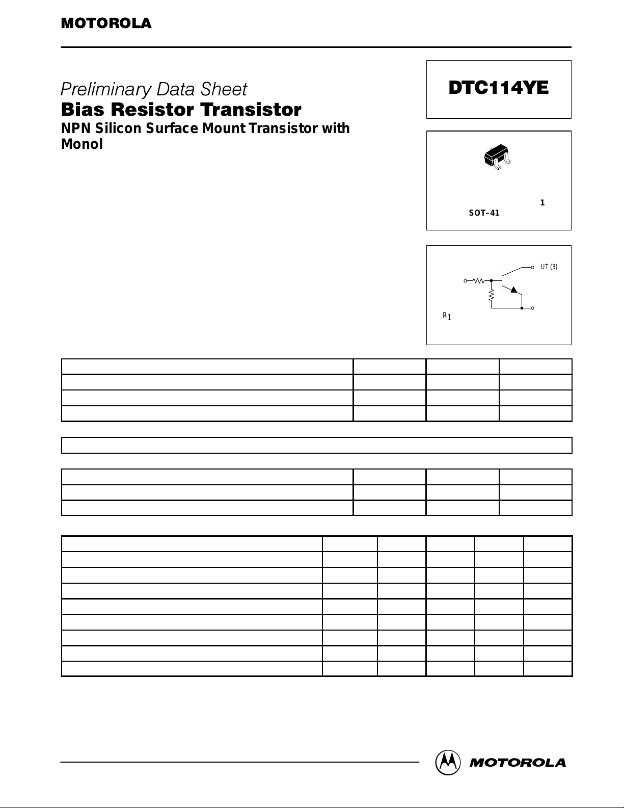
The BRT (Bias Resistor Transistor) contains a single transistor with a
monolithic bias network consisting of two resistors; a series base resistor and a
base–emitter resistor. These digital transistors are designed to replace a single
device and its external resistor bias network. The BRT eliminates these
individual components by integrating them into a single device. The DTC1 14YE
is housed in the SOT–416/SC–90 package which is ideal for low power surface
mount applications where board space is at a premium.
• Simplifies Circuit Design
• Reduces Board Space
• Reduces Component Count
• Available in 8 mm, 7 inch/3000 Unit Tape and Reel.
MAXIMUM RATINGS
Output Voltage V
Input Voltage V
Output Current I
DEVICE MARKING
DTC114YE = 69
THERMAL CHARACTERISTICS
Power Dissipation @ TA = 25°C
Operating and Storage Temperature Range TJ, T
Junction Temperature T
(TA = 25°C unless otherwise noted)
Rating Symbol Value Unit
(1)
3
2
1
CASE 463–01, STYLE 1
SOT–416/SC–90
R
IN (1)
R1 = 10 k
R2 = 47 k
O
I
O
P
D
stg
J
–55 to +150 °C
1
R
2
Ω
Ω
50 Vdc
40 Vdc
100 mAdc
*125 mW
150 °C
OUT (3)
GND (2)
ELECTRICAL CHARACTERISTICS (T
Characteristic
Input Off Voltage (VO = 5.0 Vdc, IO = 100 µAdc) V
Input On Voltage (VO = 0.3 Vdc, IO = 1.0 mAdc) V
Output On Voltage (IO = 5.0 mAdc, II = 0.25 mAdc) V
Input Current (VI = 5.0 Vdc) I
Output Cutoff Current (VO = 50 Vdc) I
DC Current Gain (VO = 5.0 Vdc, IO = 5.0 mAdc) G
Input Resistance R
Resistance Ratio R1/R
1. Device mounted on a FR–4 glass epoxy printed circuit board using the minimum recommended footprint.
This document contains information on a product under development. Motorola reserves the right to change or discontinue this product without notice.
Thermal Clad is a trademark of the Bergquist Company
REV 1
Motorola Small–Signal Transistors, FETs and Diodes Device Data
Motorola, Inc. 1996
= 25°C)
A
Symbol Min Typ Max Unit
I(off)
I(on)
O(on)
I
O(off)
I
1
2
— — 0.3 Vdc
1.4 — — Vdc
— — 0.3 Vdc
— — 0.88 mAdc
— — 500 nAdc
68 — — —
7.0 10 13 kOhms
0.17 0.21 0.25
1
DTC114YE
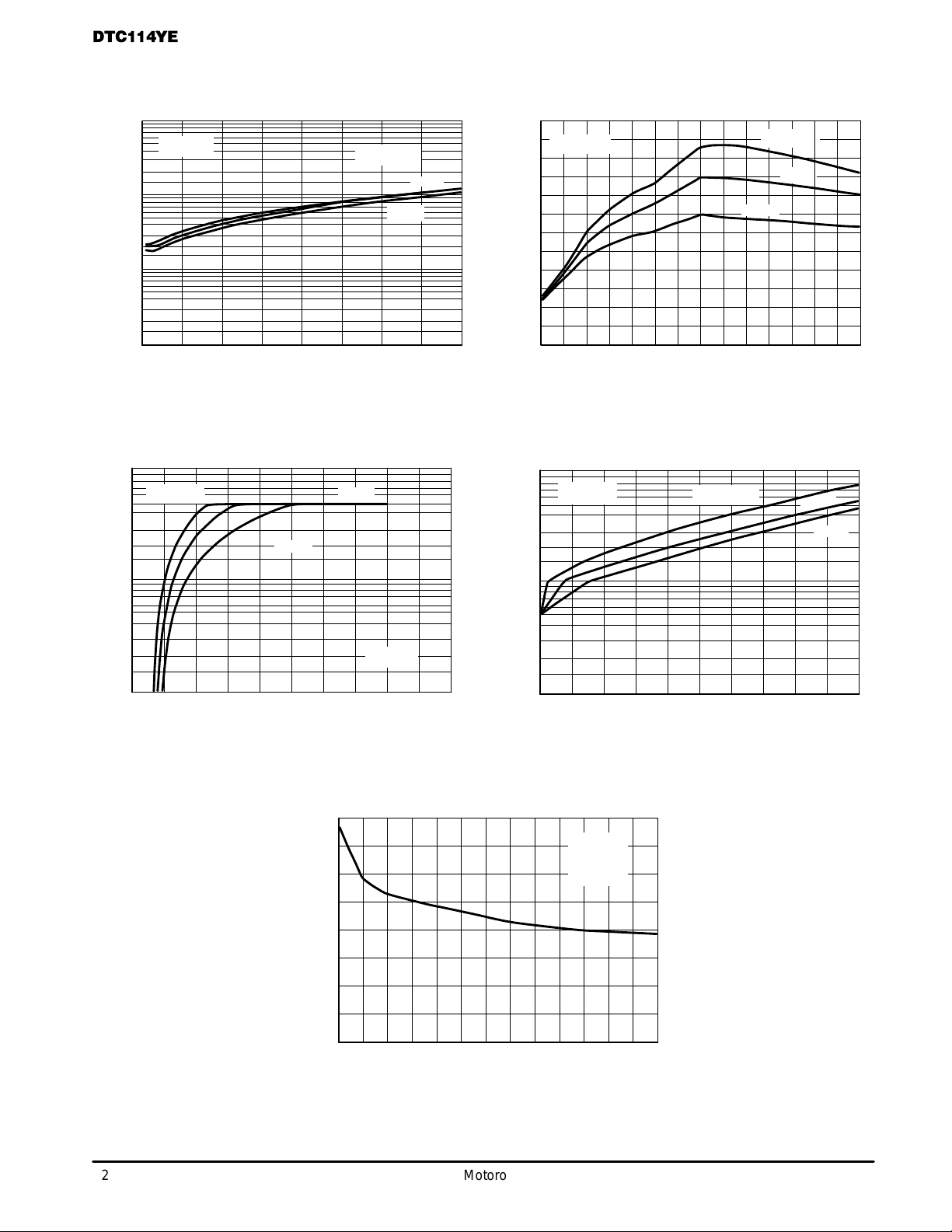
TYPICAL ELECTRICAL CHARACTERISTICS
1
IO/II = 10
0.1
, OUTPUT VOL TAGE (V)
0.01
O(on)
V
0.001
020406080
IO, OUTPUT CURRENT (mA)
Figure 1. V
100
TA=75°C
O(on)
–25°C
TA= –25°C
versus I
25°C
25°C
75°C
O
300
V
= 10
O(on)
250
200
150
100
50
, DC CURRENT GAIN (NORMALIZED)
I
G
0
2468 1520405060708090
1 10 100
IO, OUTPUT CURRENT (mA)
TA=75°C
25°C
–25°C
Figure 2. GI, DC Current Gain
10
VO = 0.2 V
TA= –25°C
25°C
75°C
10
, OUTPUT CURRENT (mA)
O
I
1
0246810
VI, INPUT VOLTAGE (V)
VO = 5 V
Figure 3. Output Current versus Input Voltage Figure 4. Input Voltage versus Output Current
4
3.5
3
2.5
2
1.5
, CAPACITANCE (pF)
ob
1
C
0.5
1
, INPUT VOLTAGE (VOLTS)
I
V
0.1
01020304050
IO, OUTPUT CURRENT (mA)
f = 1 MHz
lE = 0 V
TA = 25
°
C
0
02468101520253035404550
V
, REVERSE BIAS VOLTAGE (VOLTS)
R
Figure 5. Output Capacitance
2
Motorola Small–Signal Transistors, FETs and Diodes Device Data
 Loading...