

Page 1
Freescale Semiconductor, Inc.
MOTOROLA
SEMICONDUCTOR
Order this document
by DSP56156/D
REV 1
nc...
I
cale Semiconductor,
Frees
TECHNICAL DATA
DSP56156
DSP56156ROM
Advance Information
16-bit Digital Signal Processor
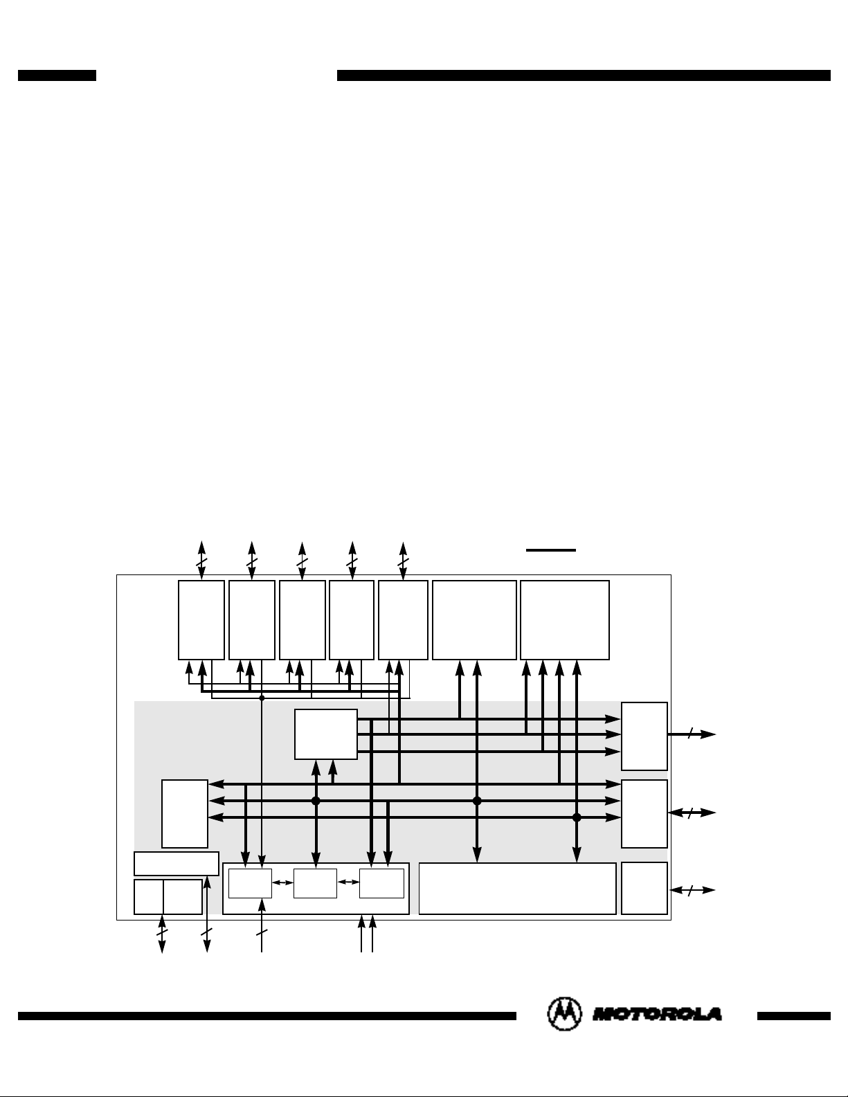
The DSP56156 is a general-purpose MPU-style Digital Signal Processor (DSP). On a single semiconductor chip, the DSP56156 comprises a very efficient 16-bit digital signal processing core, program and data memories, a number of peripherals, and system support ci rc uitry. Unique features
of the DSP56156 include a built-in sigma-delta (²ý) codec and phase-locked loop (PLL). This combination of featur es makes the DSP56156 a cost-ef fective, high-perf ormance solution for many DSP
applications, especially speech coding, digital communications, and cellular base stations.
The central processing unit of the DSP56156 is the DSP56100 core processor. Like all DSP56100based DSPs, the DSP56156 consists of three execution units operating in parallel, allowing up to
six operations to be performed during each instruct ion cycle. This parallelism gr eatly incr eases the
effective processing speed of the DSP56156. The MPU-style programming model and instruction
set allow straightforward ge neration of ef fici ent, compa ct code. The ba sic ar c hitectur es a nd devel opment tools of Motorola's 16-bit, 24-bit , and 32-bit DSPs are so similar that understanding how to
design and program one greatly reduces the time needed to learn the others.
TM
On-Chip Emulation (OnCE
ities normally available only through expensive external hardware. Development costs are reduced and in-field testing is greatly simplified using the OnCE
DSP56156 in detail.
7
Sigma-
Delta
Codec
16-bit
Timer/
Event
Counter
16-bit
56100 DSP
Core
Internal
Data
Bus
Switch
port) circuitry provi des convenient and inexpensive debug fa cil-
TM
port. Figure 1 illustrates the
5 15 2
Sync.
Serial
(SSI)
or I/O
Address
Generation
Unit
5
Sync.
Serial
(SSI)
or I/O
Host
Interface
(HI)
or I/O
Program
Memory *
2048 × 16 RAM
64 × 16 ROM
(boot)
PAB
XAB1
XAB2
GDB
PDB
XDB
Memory
2048 × 16 RAM
16-bit Bus
Data
External
Address
Bus
Switch
External
Data
Bus
Switch
Address
16
Data
16
OnCE™ Port
Clock
PLL
Gen.
3
4
Interrupt
Control
IRQ 2
Program
Decode
Controller
Program Control Unit
Program
Address
Generator
Figure 1 DSP56156 Block Diagram
Specifications and information herein are subject to change without notice.
OnCE is a trademark of Motorola, Inc.
MOTOROLA INC., 1994
For More Information On This Product,
Go to: www.freescale.com
16 x 16 + 40 —> 40-bit MAC
Data ALU
Two 40-bit Accumulators
* 12 k x 16 ROM replaces the program RAM on the DSP56156ROM
Bus
Control
Control
9
Page 2

Introduction
DSP56156 Features
DSP56156 Features
Digital Signal Processing Core
nc...
I
Memory
cale Semiconductor,
Freescale Semiconductor, Inc.
• Efficient, object code compatible, 16-bit 56100-Family DSP engine
— Up to 30 Million Instructions Per Second (MIPS) – 33 ns instruction cycle at 60 MHz
— Up to 180 Million Operations Per Second ( MOPS) at 60 M Hz
— Highly parallel instruction set wit h unique DSP a ddressing modes
— Two 40-bit accumulators i ncludi n g exte nsion b yte
— Parallel 16 × 16- bi t m u lti ply- ac cumul ate in 1 instruction cycle (2 clock cycle s)
— Double precision 32 × 3 2-b it mult iply with 72-bit result in 6 i nstruc tion c yc les
— Least Mean Square (LMS) adaptive loop filter in 2 instructions
— 40-bit Addition/Subtraction in 1 in struct ion c ycl e
— Fractional and integer arithmetic with support fo r multiprecision arithmetic
— Hardware support for block-floating poi nt FFT
— Hardware-nested DO loops including infinit e l oops
— Zero-overhead fast interrupts (2 instruction cycles)
— Three 16-bit internal data buses and three 16-bit internal address buses for
maximum information tr ansf er on - chip
• On-chip Harvard architecture permitting simultaneous accesses to program
and memories
• 2048 × 16-bit on-chip program RAM and 64 × 16-bit bootstrap ROM
(or 12 k × 16-bit on-chip program ROM on the DSP56156ROM)
• 2048 × 16-bit on-chip data RAM
• External memory expansion with 16-bit address and data buses
• Bootstrap loading from external data bus, Host Interface, or
Synchronous Serial Interface
Frees
2 DSP56156 Data Sheet MOTOROLA
Peripheral and Support Circuits
• Byte-wide Host Interface (HI) with Direct Memory Access support
• Two Synchronous Serial Interfaces (SSI) to communicate with codecs and
synchronous serial devices
— Built in µ-law and A-law compression/expansion
— Up to 32 software-selectable ti me s lots in net wo rk mode
• 16-bit Timer/Event Counter also generates and measures digital waveforms
• On-chip sigma-delta voice band Codec:
— Sampling clock rates bet we en 100 kHz and 3 MHz
— Four software-programmable decimation/interpolation ratios
2
— Internal voltage reference (
— No external components required
/5 of positive power supp ly)
For More Information On This Product,
Go to: www.freescale.com
Page 3

Freescale Semiconductor, Inc.
• On-chip peripheral registers memory mapped in data memory space
• Double buffered peripherals
• Up to 27 general purpose I/O pins
• Two external interrupt request pins
• On-Chip Emulation (OnCE™) port for unobtrusive, processor speed-independent
debugging
• Software-programmable, Phase-Locked Loop-based (PLL) f requency synthesizer for the
core clock
DSP56156 Features
Miscellaneous Features
• Power-saving Wait and Stop modes
Introduction
Documentation
nc...
I
cale Semiconductor,
Frees
• Fully static, HCMOS design for operating frequencies from 40 or 60 MHz down to DC
• 112-pin Ceramic Quad Flat Pack (CQFP) surface-mount package; 20 × 20 × 3 mm
• 112-pin Plastic Thin Quad Flat Pack (TQFP) surface-mount package; 20 × 20 × 1.5 mm
• 5 V power supply
Product Documentation
This data sheet plus the two manuals listed in Table 1 are required for a complete DSP56156
description and are necessary to properly design with the part. Documentation is available
from a local Motorola distributor, a semiconductor sales office, or through a Motorola Literature Distribution Center.
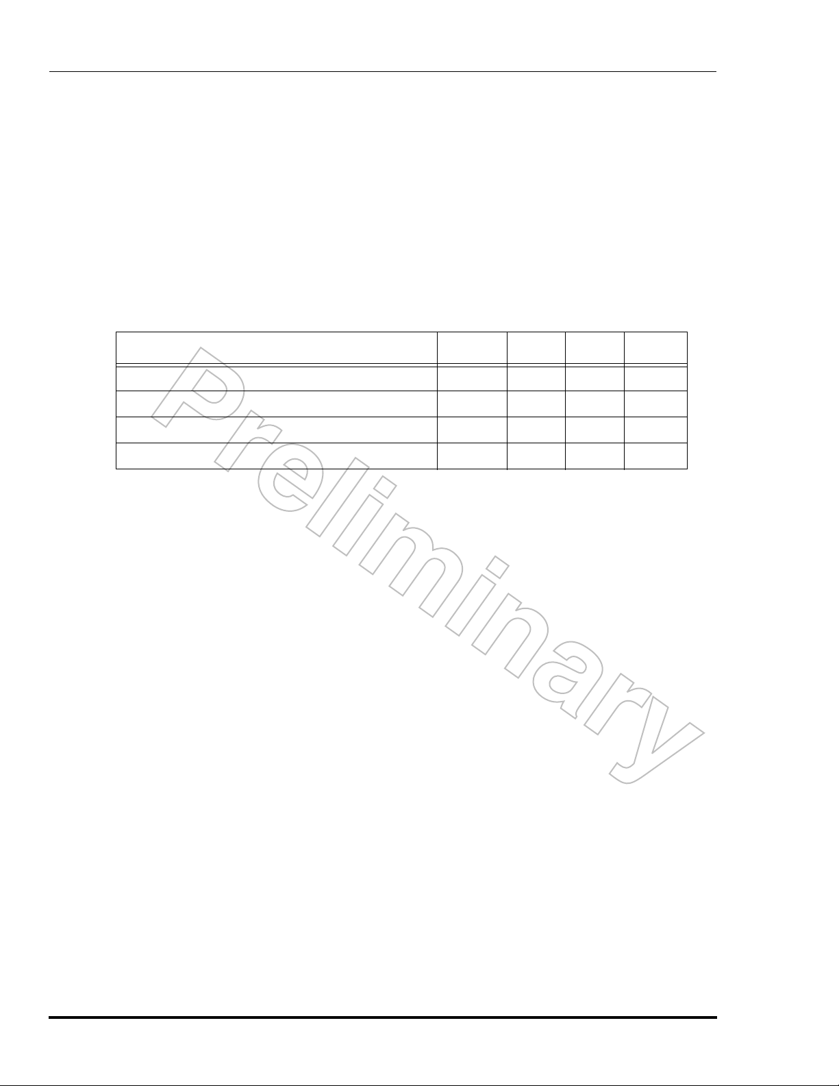
Table 1 DSP56156 Documentation
Topic Description Order Number
DSP56100 Family Manual Detailed description of the 56000-
family architecture and the 16-bit core
processor and instruction set
DSP56100FAMUM/AD
DSP56156 User’s Manual Detailed description of memory,
peripherals, and interfaces
DSP56156 Data Sheet Pin and package descriptions, and
electrical and timing specifications
MOTOROLA DSP56156 Data Sheet 3
For More Information On This Product,
Go to: www.freescale.com
DSP56156UM/AD
DSP56156/D
Page 4
Introduction
Documentation
Data Sheet Contents
Related Documentation
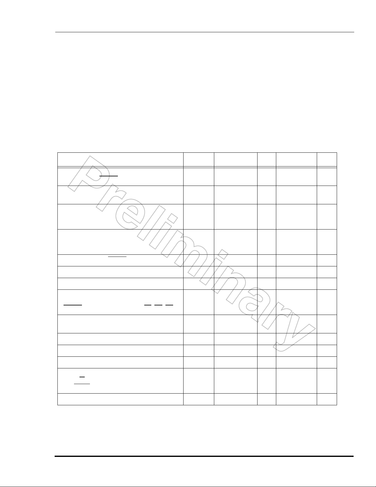
Table 2 lists additional documentation relevant to the DSP56156.
DSP Family Brochure Overview of all DSP product families BR1105/D
Freescale Semiconductor, Inc.
Table 2 Related Motorola Documentation
Topic Description Order Number
Development Tools Product Brief. Includes ordering
information
nc...
I
cale Semiconductor,
Fractional and Integer Arithmetic Application Report. Includes code APR3/D
Fast Fourier Transforms (FFTs) Application Report. Comprehensive
FFT algorithms and code for
DSP56001, DSP56156, and
DSP96002
G.722 Audio Processing Application Report. Theory and code
using SB-ADPCM
Dr. BuB Bulletin Board Flyer. Motorola’s electronic bulletin
board where free DSP software is
available
Third Party Compendium Brochures from companies selling
hardware and software that supports
Motorola DSPs
University Support Program Flyer. Motorola’s program that sup-
ports universities in DSP research
and education
DSPTOOLSP/D
APR4/D
APR404/D
BR297/D
DSP3RDPTYPAK/D
BR382/D
Frees
Data Sheet Contents
This data sheet contains:
• signal definitions and pin locations
• electrical specifications and timings
• package descriptions
• design considerations
• order ing inform ation
4 DSP56156 Data Sheet MOTOROLA
For More Information On This Product,
Go to: www.freescale.com
Page 5
Freescale Semiconductor, Inc.
Introduction
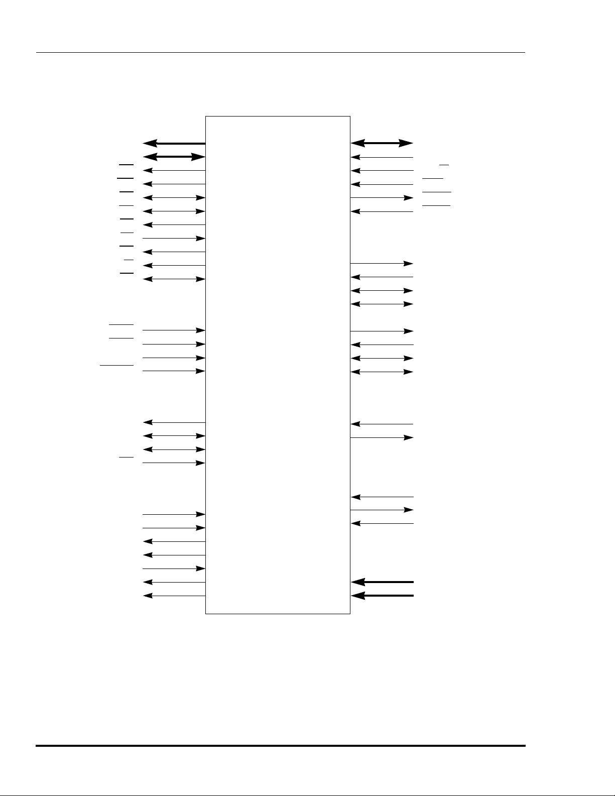
Pin Groupings
Pin Groupings
The DSP56156 is available in a 112-pin Cerami c Quad Flat P ack ( CQFP ) and a 112- pin Pla stic
Thin Quad Flat Pack (TQFP). The input and output signals are organized into the functional
groups indicated in Table 3. Figure 2 illustrates the chip’s pin functions.
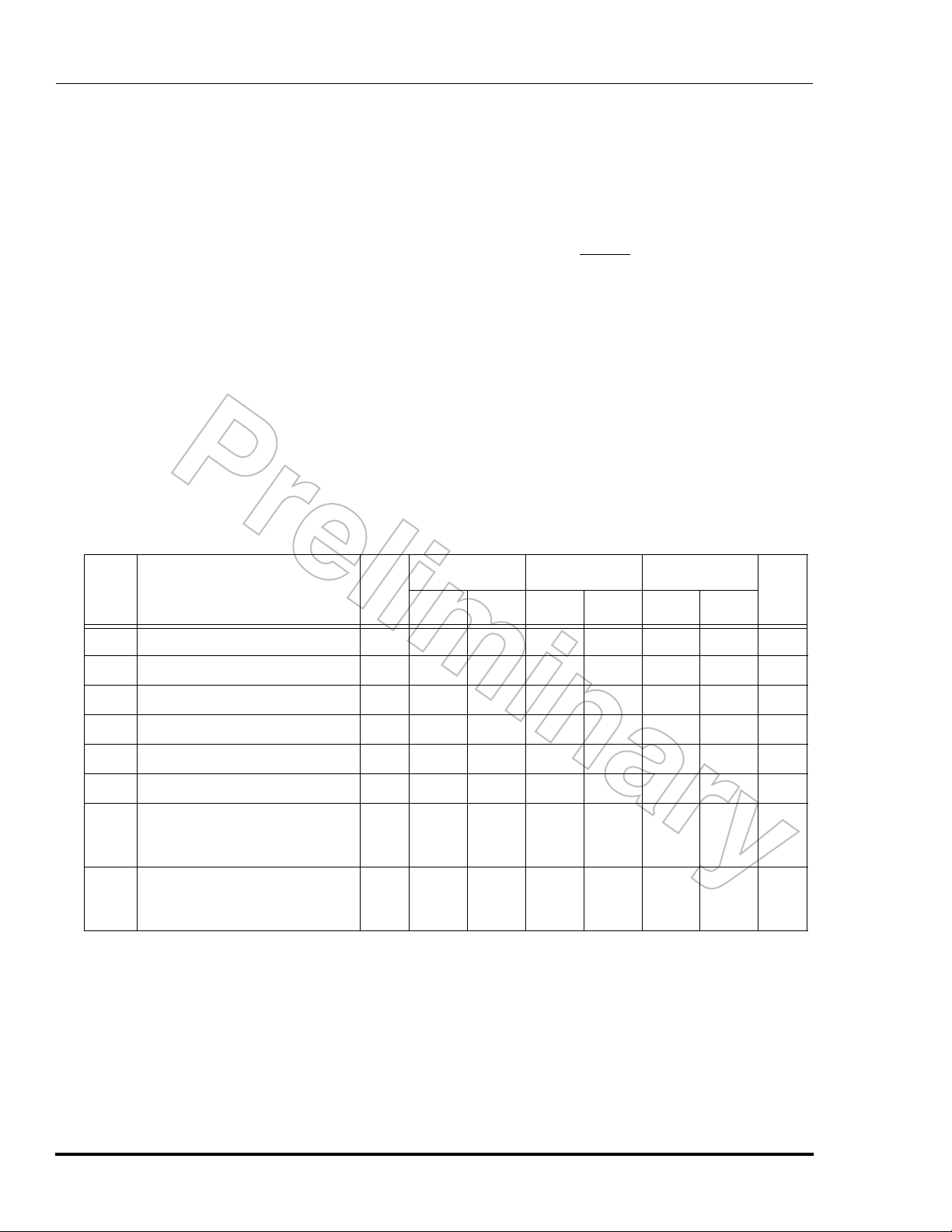
Table 3 Functional Pin Groupings
Functional Group Number of Pins
Address 16
nc...
I
Data Bus 16
cale Semiconductor,
Frees
Bus Control 9
Host Interface (HI) 15
Synchronous Serial Interfaces (SSI) 10
Timer Interface 2
Interrupt and Mode Control 4
Phase-Locked Loop (PLL) and Clock 3
TM
On-Chip Emulation (OnCE
On-Chip Codec 7
Power (V
Ground (GND) 16
Total 112
NOTE: OVERBARS are used throughout this document to indicate a signal which is at Ground voltage (typi-
cally a TTL logic low — V
V
voltage (typically a TTL logic high — VIH or VOH) when the function is logically false.
CC
)10
CC
or VOL) when the function is logically true. These signals are, likewise, at
IL
Port) 4
MOTOROLA DSP56156 Data Sheet 5
For More Information On This Product,
Go to: www.freescale.com
Page 6
Introduction
Pin Functions
nc...
I
cale Semiconductor,
Frees
A0-A15
D0-D15
RD
WR
BR
BG
BS
TA
PS/DS
R/W
BB
MODA/IRQA
MODB/IRQB
MODC
RESET
DSO
DSI/OS0
DSCK/OS1
DR
MIC
AUX
SPKP
SPKM
BIAS
VREF
VDIV
Freescale Semiconductor, Inc.
DSP56156
H0-H7*
HA0-HA2*
HR/W*
HEN*
HREQ*
HACK*
STD0*
SRD0*
SCK0*
SC00-SC10*
STD1*
SRD1*
SCK1*
SC01-SC11*
TIN*
TOUT*
EXTAL
CLKO
SXFC
V
GND
External
Bus
Interrupt/
Mode
Control
On-Chip
Emulator
(OnCE)
Port
On-Chip
Codec
Host
Interface (HI)
Two
Synchronous
Serial
Interfaces
(SSI)
Timer/Event
Counter
Clock
and
Phase-locked
Loop
(PLL)
112 pins
CC
* These pins have an alternate function of general purpose input/output.
Figure 2 DSP56156 Pin Functions
6 DSP56156 Data Sheet MOTOROLA
For More Information On This Product,
Go to: www.freescale.com
Page 7

Freescale Semiconductor, Inc.
Pin Descriptions
Address and Data Bus
Bus Control
nc...
I
cale Semiconductor,
Frees
Pin Descriptions
Address and Data Bus
A0-A15 (Address Bus) — three-state, active
high outputs. A0-A15 change in t0 and
specify the address for external program and data memory accesses. If
there is no external bus activity, A0-A15
remain at their previous values. A0-A15
are three-stated during hardware reset.
D0-D15 (Data Bus) — three-state, active
high, bidirectional input/outputs.
Read data is sampled on the trailing
edge of t2, while write data o utput is
enabled by the leading edge of t2 and
three-stated at the leading edge of t0. If
there is no externa l bus activity, D0-D15
are three-stated. D0-D15 are also threestated during hardware reset.
Bus Control
PS/DS (Program/Data Memory Select) —
three-state, active low output. This out-
put is asserted only when external data
memory is referenced. PS/DS
the same for the A0-A15 address lines.
is high for program memory ac-
PS/DS
cess and is low for data memory access. If
the external bus is not used during an instruction cycle (t0, t1, t2, t3), PS/DS
high in t0. PS/DS
ance state during hardware reset.
(Read/Write) — three-state, active
R/W
low output. Timing is the same as the
address lines, providing an “early
write” signal. R/W
t0) is high for a read access and is low
for a write access. If the external bus is
not used during an instruction cycle
is in the high imped-
(which changes in
timing is
goes
(t0, t1, t2, t3), R/W
is three-stated during hardware reset.
(Write Enable) — three-st ate, active
WR
low output. This output is asserted during external memory write cycles. When
is asserted in t1, the data bus pins
WR
D0-D15 become outputs and the DSP
puts data on the bus during the leading
edge of t2. When WR
the external data has been latched inside
the external device. When WR
ed, it qualifies the A0-A15 and PS/DS
pins. WR can be connected directly to
the WE
stated during hardware reset or when
the DSP is not bus master.
(Read Enable) — three-st ate, active
RD
low output. This output is asserted
during external memory read cycles.
When RD
the data bus pins D0-D15 become inputs and an external device is enabled
onto the data bus. When RD
serted in t3, the external data is latched
inside the DSP. When RD
qualifies the A0-A15 and PS/DS
RD
OE
three-stated during hardware reset or
when the DSP is not bus master.
(Bus Strobe) — three-state, active
BS
low output. Asserted at the start of a
bus cycle (during t0) and deasserted at
the end of the bus cycle (during t2).
This pin provides an “early bus start”
signal which can be used as address
latch and as an “e arly bus end” signa l
which can be used by an external bus
controller. BS
hardware reset.
pin of a static RAM. WR is three-
is asserted in late t0/early t1,
can be connected directly to the
pin of a stat ic RA M or ROM. RD is
goes high in t0. R/W
is deasserted in t3,
is asserted, it
is three-stated during
is assert-
is deas-
pins.
MOTOROLA DSP56156 Data Sheet 7
For More Information On This Product,
Go to: www.freescale.com
Page 8
Pin Descriptions
Bus Control
Freescale Semiconductor, Inc.
nc...
I
cale Semiconductor,
Frees
TA (Transfer Acknowledge) — active
low input. If there is no external bus ac-
tivity, the TA
DSP. When there is external bus cycle
activity, TA
states in the external bus cycle. TA
sampled on the leading edge of the
clock. Any numb er of wait stat es f rom 1
to infinity may be inserted by using TA
is sampled high on the leading
If TA
edge of the clock beginning the bus cycle, the bus cycle will end 2T after the
has been sampled low on a leading
TA
edge of the clock; if the Bus Control Register (BCR) value does not program
more wait states. The number of wait
states is determined by the TA
by the Bus Control Register (BCR),
whichever is longer. TA
during the leading edge of the clock
when wait states are controlled by the
BCR value. In that case, TA
be sampled low during the leading edge
of the last period of the bus cycle programmed by the BCR (2T before the end
of the bus cycle programmed by the
BCR) in order not to add any wait states.
should always be deasserted during
TA
CLKO
TA
input is ignored by the
can be used to insert wait
is still sampled
will have to
T0
T1 T2
T3
T0
T1 T2
is
input or
T2
Tw
.
T3 T0
T1
t3 to be sampled high by the leading
edge of T0. If TA
ed) at the leading edge of the t0 beginning the bus cycle, and if no wait states
are specified in the BCR register, zero
wait states will be i nserte d in the external bus cycle, regardless the status of
during the leading edge of T2.
TA
(Bus Request) — active low output
BR
when in master mode, active low input when in slave mode. After power-
on reset, this pin is an input (slave
mode). In this mode, the bus request
allows another device such as a pro-
BR
cessor or DMA controller to become
the master of the DSP external data
bus D0-D15 and external address bus
A0-A15. The DSP asserts BG
states after the BR
The DSP bus controller releases control
of the external data bus D0-D15, address bus A0-A15 and bus control pins
PS/DS
est time possible consistent w ith proper synchronization. These pins are then
placed in the high impedance state and
T2
T3 T0
, RD, WR, and R/W at the earli-
T1
is sampled low (assert-
input is asserted.
T2
Tw T2
Tw
T2
T3
a few T
BS
CLKO
TA
BS
T0
T1 T2
Tw
T2
Tw T2
Tw
T2
T3 T0
T1
T2
Tw T2
Tw
T2
T3 T0
T1
T2
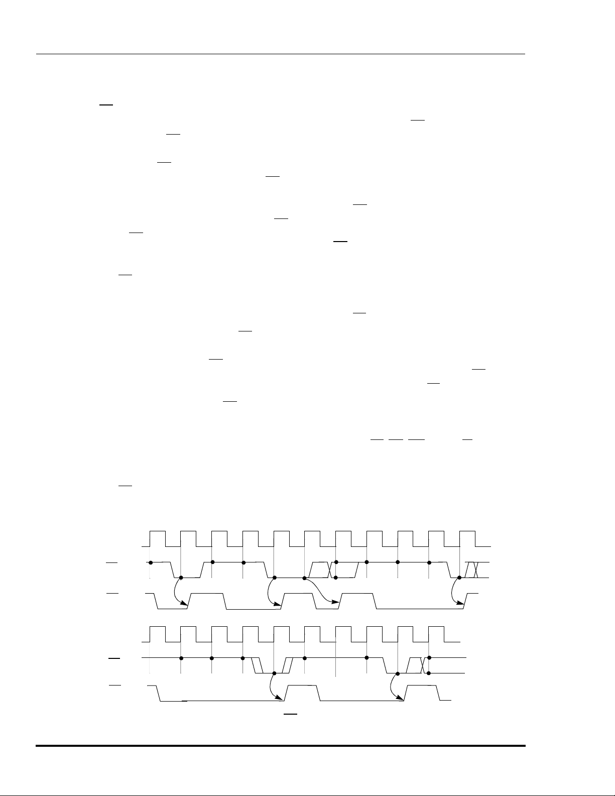
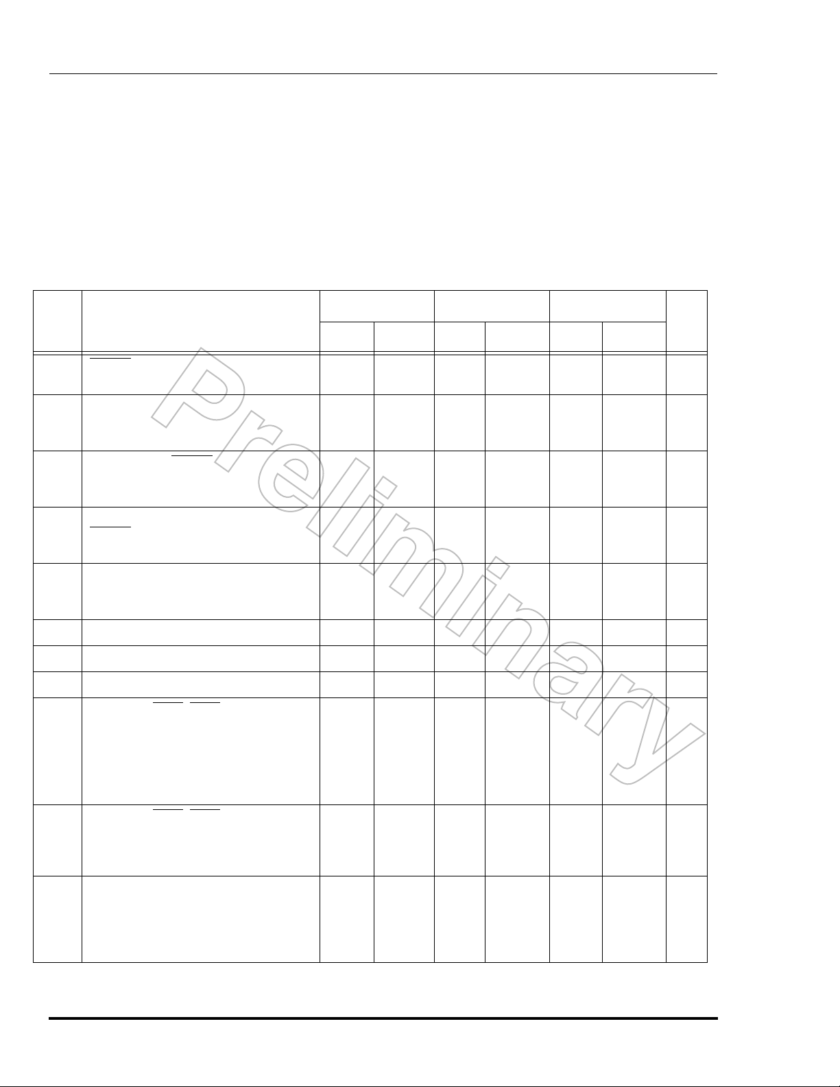
Figure 3 TA Controlled Accesses
8 DSP56156 Data Sheet MOTOROLA
For More Information On This Product,
Go to: www.freescale.com
Page 9

Freescale Semiconductor, Inc.
Pin Descriptions
Bus Control
nc...
I
cale Semiconductor,
Frees
the BB pin is deasserted. The DSP continues executing instructions only if internal program and data memory
resources are accessed. If the DSP requests the external bus while BR
pin is asserted, the DSP bus controller
inserts wait states until the external bus
becomes available (BR
serted). Note that interrupts are not
serviced when a DSP instruction is
waiting for the bus controller. Note
also that BR
rupting the execution of a read/ modify/write instruction.
If the master bit in the OMR register is
set, this pin becomes an output (Master
Mode). In this mode, the DSP is not the
external bus master and has to assert
to request the bus mastership. The
BR
DSP bus controller will insert wait
states until BG
will then begin normal bus accesses after the rising of the clock which sampled BB
remain asserted until the DSP no longer needs the bus. In this mode, the Request Hold bit (RH) of the Bus Control
Register (BCR) allows BR
under software control.
During external accesses caused by an
instruction executed out of external program memory, BR
for consecutive external X memory accesses and continues toggling for consecutive external P memory accesses
unless the Request Hold bit (RH) is set
inside the Bus Control Register (BCR).
In the master mode, BR
used for non arbitration purpose: if BG
is always asserted, BR is asserted in t0
of every external bus access. It can then
be used as a chip select to turn a exter-
is prevented from inter-
input is asserted and
high. The BR output signal will
and BB deas-
to be asserted
remains asserted low
can also be
input
nal memory device off and on between
internal and external bus accesses. BR
timing is in that case similar to A0-A15,
and PS/DS; it is asserted and
R/W
deasserted during t0.
(Bus Grant) — active low input when
BG
in master mode, active low output
when in slave mode. Output after
power on reset if the slave is selected,
this pin is asserted to acknowledge an
external bus request. It indicates that
the DSP will release control of the external address bus A0-A15, data bus
D0-D15 and bus control pins when BB
is deasserted. The BG output is asserted in response to a BR
output is asserted and BB is deas-
BG
serted, the external address bus A0-A15,
data bus D0-D15 and bus control pins
are in the high impedance state. BG
sertion may occur in the middle of an
instruction which requires more than
one external bus cycle for execution.
Note that BG
during indivisible read-modify-write
instructions (BFSET, BFCLR, BFCHG).
When BR
is deasserted and the DSP regains control of the external address bus, data
bus, and bus control pins when the BB
pin is sampled high.
This pin becomes an input if the master
bit in the OMR register is set (Master
Mode). It is asserted by an external processor when the DSP may become the
bus master. The DSP can start normal
external memor y access af ter the BB
has been deasserted by the previous
bus master. When BG
DSP will release the bus as soon as the
current transfer is com plete d. The s tate
may be tested by testing the BS bit
of BG
in the Bus Control Register. BG
nored during hardware reset.
assertion will not occur
is deasserted, the BG output
input. When the
is deasserted, the
as-
pin
is ig-
MOTOROLA DSP56156 Data Sheet 9
For More Information On This Product,
Go to: www.freescale.com
Page 10

Pin Descriptions
Bus Control
Interrupt and Mode Control
Freescale Semiconductor, Inc.
nc...
I
cale Semiconductor,
Frees
BB (Bus Busy) — active low input when
not bus master, active low output
when bus master. This pin is asserted
by the DSP when it becomes the bus
master and it performs an external access. It is deasserted when the DSP releases bus mastership. BB
input when the DSP is no longer the
bus master.
becomes an
Interrupt and Mode Control
MODA/IRQA (Mode Select A/External In-
terrupt Request A) — input. This in-
put has two functions:
•to select the initial chip operating
mode and,
•to allow an external device to request
a DSP interrupt after internal synchronization.
MODA is read and internally latched
in the DSP when the processor exits the
reset state. MODA and MODB select
the initial chip operating mode. Several
clock cycles after leaving the reset state,
the MODA pin changes to the external
interrupt request IRQA
ating mode can be changed by software after reset.
The IRQA
ternal interrupt request which indicates that an external device is
requesting service. It may be programmed to be level sensitive or negative edge triggered. If level sensitive
triggering is selected, an external pull
up resistor is required for wired-OR
operation. If the processor is in the stop
standby state and IRQA
processor will exit the stop state.
input is a synchronized ex-
. The chip oper-
is asserted, the
MODB/IRQB
MODC ( Mode Select C) — input. This input
RESET
(Mode Select B/External In-
terrupt Request B) — input. This in-
put has two functions:
•to select the initi al chip operating
mode and,
•to allow an external device to request
a DSP interrupt after internal synchronization.
MODB is read and internally latched in
the DSP when the processor exits the
reset state. MODA and MODB select
the initial chip operating mode. Several
clock cycles after leaving the reset state,
the MODB pin changes to the external
interrupt request IRQB
chip operating mode can be changed
by software.
The IRQB
request which indicates that an external device is requesting service. It may
be programmed to be level sensitive or
negative edge triggered. If level sensitive triggering is selected, an external
pull up resistor is required for wiredOR operation.
selects the initial bus operating mode.
When tied high, the external bus is programmed in the master mode (BR
put and BG
the bus is programmed in the slave
mode (BR
MODC is read and internally latched in
the DSP when the processor exits the
reset state. After RESET
ing mode can be changed by software by
writing the MC bit of the OMR register.
(Reset) — input. This input is a direct
hardware reset of the processor. When
RESET
and placed in the reset state. A Schmitt
input is an external interrupt
input) and when tied low
input and BG output).
is asserted, the DSP is initialized
. After reset, the
, the bus operat-
out-
10 DSP56156 Data Sheet MOTOROLA
For More Information On This Product,
Go to: www.freescale.com
Page 11

Freescale Semiconductor, Inc.
Pin Descriptions
Interrupt and Mode Control
Host Interface
nc...
I
cale Semiconductor,
Frees
trigger input is u sed for nois e immuni ty .
When the reset pin is deasserted, the initial chip operating mode is latched from
the MODA and MODB pins, and the initial bus operating mode is latched from
the MODC pin. The internal reset signal
should be deasserted synchronized with
the internal clocks.
Host Interface
H0-H7 (Host Dat a Bu s) — bidirectional. This
bidirectional data bus is used to transfer
data between the host processor and the
DSP. This bus is an input unless enabled
by a host processor read. H0-H7 may be
programmed as Port B general purpose
parallel I/O pins called PB0 -PB7 when
the Host Interface (HI) is not being used.
HA0-HA2 (Host Address 0-2) — input*. These
inputs provide the address selection
for each HI register and are stable
when HEN
be programmed as Port B general purpose parallel I/O pins called PB8-PB10
when the HI is not being used.
(Host Read/Write) — input*. Th is in-
HR/W
put selects the direction of data transfer
for each host processor access. If HR/W
is high and HEN is asserted, H0-H7 are
outputs and DSP data is transferred to
the host processor. If HR/W
HEN
host data is transferred to the DSP.
When HEN
HR/W
eral purpose I/O pin called PB11
when the HI is not being used.
is asserted. HA0-HA2 may
is low and
is asserted, H0-H7 are inputs and
is asserted, HR/W is stable.
may be programmed as a gen-
HEN
(Host Enable) — input*. This input en-
ables a data transfer on the host data
bus. When HEN
is high, H0-H7 becomes an output a nd
DSP data may be latched by the host
processor. When HEN
HR/W
host data is latched inside the DSP
when HEN
chip select signal derived from host address decoding and an enable clock is
connected to the Host Enable. HEN
may be programmed as a general purpose I/O pin called PB12 when the HI
is not being used.
(Host Request) — output*. This open-
HREQ
drain output signal is used by the HI to
request service from the host processor. HREQ
terrupt request pin of a host processor,
a transfer request of a DMA controller,
or a control input of external ci rcuitry.
HREQ
quest occurs in the HI. HREQ
serted when the enabled request is
cleared or masked, DMA HACK is asserted, or the DSP is reset. HREQ
be programmed as a general purpose
I/O pin (not open-drain) called PB13
when the HI is not being used.
(Host Acknowledge) — input*. This
HACK
input has two functions:
If programmed as a host acknowledge
signal, HACK
strobe for HI DMA data transfers. If programmed as an MC68000 ho st interrupt
is low, H0-H7 is an input and
is asserted when an enabled re-
•to provide a host acknowledge signal
for DMA transfers and,
•to control handshaking and to provide a host interrupt acknowledge
compatible with MC68000 family
processors.
is asserted and HR/W
is asserted and
is deasserted. Normally a
may be connected to an in-
may be used as a data
is deas-
may
* These pins can be bidirectional when programmed as general purpose I/O.
MOTOROLA DSP56156 Data Sheet 11
For More Information On This Product,
Go to: www.freescale.com
Page 12

Pin Descriptions
16-bit Timer
SSI
Freescale Semiconductor, Inc.
nc...
I
cale Semiconductor,
Frees
acknowledge, HACK enables the HI
Interrupt Vector Register (IVR) onto
the host data bus H0-H7 if the Host Request HREQ
case, all other HI control pins are ignored and the HI state is not affected.
HACK
eral purpose I/O pin called PB14 when
the HI is not being used.
output is asserted. In this
may be programmed as a gen-
16-bit Timer
TIN (Timer Input) — input*. This input re-
ceives external pulses to be counted by
the on-chip 16-bit timer when external
clocking is selected. The pulses are internally synchronized to the DSP core
internal clock. TIN may be programmed as a general purpose I/O pin
called PC10 when the external event
function is not being used.
TOUT (Timer Output) — output*. This out-
put generates pulses or toggles on a
timer overflow event or a compare
event. TOUT may be programmed as a
general purpose I/O pin called PC11
when disabled by the timer out enable
bits (TO2-TO0).
Synchronous Serial Interfaces (SSI)
PC0 and PC5, respectively, when the
STD function is not being used.
SRD0-1 (SSI0-1 Receive Data) — input*.
These input pins receive serial data and
transfer the data to the SSI0-1 Receive
Shift Register. SRD0 and SRD1 may be
programmed as a general purpose I/O
pin called PC1 and PC6, respectively,
when the SRD function is not being
used.
SCK0-1 (S SI0-1 Serial Clock) — bidirection-
al. These bidirectional pins provide the
serial bit rate clock for the SSI0-1 interface. SCK0 and SCK1 may be programmed as a general purpose I/O pin
called PC2 and PC7, respectively,
when the SSI0-1 interfaces are not being used.
SC10-11 (SSI0-1 Serial Control 1) — bidirec-
tional. These bidirectional pins are
used by the SSI0-1 serial interface as
frame sync I/O or flag I/O. SC10 and
SC11 may be programmed as a gene ral
purpose I/O pin called PC3 and PC8,
respectively, when the SSI0-1 are not
using these pins.
SC00-01 (SSI0-1 Serial Control 0) — bidirec-
tional. These bidirectional pins are
used by the SSI0-1 serial interface as
frame sync I/O or flag I/O. SC00 and
SC01 may be programmed as a gene ral
purpose I/O pin called PC4 and PC9,
respectively, when the SSI0-1 are not
using these pins.
STD0-1 (SSI0-1 Transmit Data) — output*.
These output pins transmit seri al data
from the SSI 0-1 Transm it Shift R egister.
STD0 and STD1 may be programmed
as a general purpose I/O pin called
* These pins can be bidirectional when programmed as general purpose I/O.
12 DSP56156 Data Sheet MOTOROLA
For More Information On This Product,
Go to: www.freescale.com
Page 13

Freescale Semiconductor, Inc.
Pin Descriptions
OnCE
On-Chip Codec
nc...
I
cale Semiconductor,
Frees
On-Chip Emulation
TM
(OnCE
DSI/OS0 (Debug Serial Input/Chip Status 0) —
DSCK/OS1 (Debug Serial Clock/Chip Status 1)
DSO (Debug Serial) — output. The debug
Port)
bidirectional. The DSI/OS0 pin, when
an input, is the pin through which serial data or commands are provided to
the OnCE port controller. The data received on the DSI pin will be recognized only when the DSP has entered
the debug mode of operation. Data
must have valid TTL logic levels before
the serial clock falling edge. Data is always shifted into the OnCE serial port
most significant bit (MSB) first. When the
DSP is not in the debug mode, the DSI /
OS0 pin provides information about the
chip status if it is an output and used in
conjunction with the OS1 pin.
— bidirectional. The DSCK/OS1 pin,
when an input, is the pin through
which the serial clock is supplied to the
OnCE port. The serial clock provides
pulses required to shift data into and
out of the OnCE serial port. Data is
clocked into the OnCE port on the falling edge and is clocked out of the
OnCE serial port on the rising edge. If
the DSCK/OS1 pin is an output and
used in conjunction with the OS0 pin, it
provides information about the chip
status when the DSP is not in the debug
mode.
serial output provides the data contained in one of the OnCE port con troller registers as specified by the last
command received from the command
controller. When idle, this pin is high.
When the requested data is available, the
DSO line will be asserted (negative true
logic) for four T cycles (one instruction
cycle) to indicate that the serial sh ift register is ready to receive clocks in order to
deliver the data. When the chip enters
the debug mode du e to an external debug request (DR
debug request (DEBUG), a hardware
breakpoint occurrence or a trace/step
occurrence, this l ine will be assert ed for
three T cycles to indicate that the chip
has entered the debug mode and is waiting for commands. Data is always shifted out the OnCE serial port with the
most significant bit first.
(Debug Request) — input. The debug
DR
request input provides a means of entering the debug mode of operation.
This pin, when asserted, will cause the
DSP to finish the current instructio n being executed, enter the debug mode,
and wait for commands to be entered
from the debug serial input line.
), an internal software
On-Chip Codec
AUX (Auxiliary) — input. This pin is select-
ed as the analog input to the A/D converter when the INS bit is set in the
codec control register COCR. This pin
should be left floating when the codec
is not used.
BIAS (Bias current) — input. This input is
used to determine the bias current for
the analog circuitry. Connecting a resistor between BIAS and GNDA will
program the current bias generator.
This pin should be left floating when
the codec is not used.
MIC (Microphone) — input. This pin is se-
lected as the analog input to the A/D
converter when the INS bit is cleared in
MOTOROLA DSP56156 Data Sheet 13
For More Information On This Product,
Go to: www.freescale.com
Page 14

Pin Descriptions
On-Chip Codec
Power, Ground, and Clock
Freescale Semiconductor, Inc.
nc...
I
cale Semiconductor,
Frees
the codec control register COCR. This
pin should be left floa ting when the codec is not used.
SPKP (Speaker Plus) — output. This pin is
the positive analog output from the onchip D/A converter. This pin should be
left floating when the codec is not used.
SPKM (Speaker Minus) — output. This pin is
the negative analog output from the
on-chip D/A converter. This pin
should be left floating when the codec
is not used.
VREF (Voltage Reference) — output. This
pin is the op-amp buffer output in the
reference voltage generator. It has a
value of (
ways be connected to the GNDA
through two capacitors, even when the
codec is not used.
VDIV (Voltage Division) — output. This
output pin is also the output to the onchip op-amp buffer in the reference
voltage generator. It is connected to a
resistor divider network located within
the codec block which provides a voltage equal to (
be connected to the GND via a capacitor
when the codec is used and should be
left floating when the codec is not used.
2
/
)V
. This pin should al-
CCA
5
2
/
)V
. This pin shou ld
CCA
5
Power, Ground, and Clock
VCC(Power) — Power pins
GND (Ground) — Ground pins
(Synthesizer Power) — This pin sup-
V
CCS
plies a quiet power source to the PhaseLocked Loop (PLL) to provide greater
frequency stability.
GNDS (Synthesizer Ground) — This pin sup-
plies a quiet ground source to the PLL
to provide greater frequency stability.
V
(Analog Power) — This pin is the posi-
CCA
tive analog supply input. It should be connected to V
GNDA (Analog Ground) — This pin is the an-
alog ground return. It should be connected to digital GND when the codec
is not used.
EXTAL (External Clock) — input. This input
should be driven by an external clock or
by an external oscillator. After being
squared, the input frequency can be
used as the DSP core internal clock. In
that case, it is divided by two to produce
a four phase instruction cycle cl ock, t he
minimum inst ruction t ime being t wo input clock periods. Th is i nput frequen cy
is also used, after division, as input
clock for the on-chip codec and the onchip PLL.
CLKO (Clock Output) — output. This pin
outputs a buffered clock signal. By programming two bits (CS1-CS0) inside
the PLL Control Register (PLCR), the
user can select between outputting a
squared version of the signal applied to
EXTAL, a squared version of the signal
applied to EXTAL divided by 2, and a
delayed version of the DSP core master
clock. The clock frequency on this pin
can be disabled by setting the Clockout
Disable bit (CD; bit 7) of the Operating
Mode Register (OMR). When disabled,
the pin can be left floating.
SXFC (External Filter Capacitor) — This pin
adds an external capacitor to the PLL
filter circuit. A low leakage capacitor
should be connected between and located very close to SXFC and V
when the codec is not used.
CC
CCS
.
14 DSP56156 Data Sheet MOTOROLA
For More Information On This Product,
Go to: www.freescale.com
Page 15
Freescale Semiconductor, Inc.
Electrical Characteristics and Timing
Electrical Characteristics and Timing
nc...
I
cale Semiconductor,
Frees
CAUTION:
The DSP56156 is fabricated in high density HCMOS with TTL compatible inputs and CMOS
compatible outputs.
Supply Voltage V
All Input Voltages V
Current Drain per Pin ex cludi ng V
Storage Temperature T
Exceeding maximum electrical ratings will permanently damage or
disable the chip, or impair the chip’s long term reliability.
Table 4 Maximum Electrical Ratings (GND = 0 Vdc)
Rating Symbol Value Unit
CC
IN
and GND I 10 mA
CC
stg
Table 5 Operating Conditions
Supply Voltage
V
CC
Min Max Min Max
4.5 5.5 -40 115
Table 6 Thermal Characteri stics of CQFP and TQFP Packages
Junction Temperature
(°C)
T
J
-0.3 to +7.0 V
GND - 0.5 to VCC + 0.5 V
-55 to +150 °C
Thermal Resistance
Characteristics
Junction to Ambient Θ
Junction to Case (estimated) Θ
NOTE: This device contains protective circuitry to guard against damage due to high static voltage or electrical
fields. Howeve r, normal precaution s are advised to av oid application o f any voltages hi gher than maximu m
rated voltages to t his high-i mpedance c ircuit. R eliabili ty of opera tion is en hanced if unused in puts ar e tied
to an appropriate logic voltage level (e.g., either GND or V
MOTOROLA DSP56156 Data Sheet 15
For More Information On This Product,
Go to: www.freescale.com
Symbol
JA
JC
CC
Value
Rating
CQFP TQFP
40 49 °C/W
78°C/W
).
Page 16
Electrical Charac teristics and Timing
Analog I/O Characteristics
Analog I/O Characteristics
(V
= 5.0 V dc ± 10%, TJ = -40° to +125°C)
CC
A
The analog I/O characteristics of this device are listed in Ta ble 7.
For additional information regarding the use of analog signals, see “Design Considerations”
at the end of this document.
Characteristic Min Typ Max Unit
Input Impedance on MIC and AUX (See Note 1) 46 78 1400 kΩ
nc...
I
Input Capacitance on MIC and AUX ——10pF
Peak Input Voltage on the MIC/AUX Input for Full Scale
Linearity (0.14 dBm0): 6 dB - MGS1 - 0 = 00
(See Note 2) 0 dB - MGS1 - 0 = 01
Freescale Semiconductor, Inc.
Table 7 Analog I/O Characteris ti cs
6 dB - MGS1 - 0 = 10
17 dB - MGS1 - 0 = 11
—
—
—
—
—
—
—
—
1.414
0.707
354
100
Vp
Vp
mVp
mVp
cale Semiconductor,
Frees
Internal Input Gain Variation;
G = -6 dB, 0 dB, 6 dB or 17 dB
(±0.83 dB variation due to 10% variation on V
VREF Output Voltage 1.8 2 2.2 V
VREF Output Current — — ±1 mA
DC Offset Between SPKP and SPKM — — 100 mV
Allowable Differential Load Capacitance on
SPKP and SPKM (with 1 kΩ in series)
Allowable Single-ended Load Capacitance on
SPKP or SPKM (with 0.5 kΩ in series)
Maximum Single-ended Signal Output Level — — 1 Vp
Maximum Differential Signal Output Level — — 2 Vp
Single-ended Load Resistance 500 — — Ω
Differential Load Resistance 1 — — kΩ
Resistance BIAS — 10
Internal Output Volume Control Variation
VC = -20, -15, -10, -5, 0, 6, 12, 18, 24, 30, 35 dB
(± 0.83 dB variation due to 10% variation on V
CC
CC
):
)
G - 0.83 G G + 0.83 dB
0 — 0.05 µF
0
(See Note 3)
VC - 0.83 VC VC + 0.83 dB
— 100
0.1
—kΩ
(See
Note 4)
µF
NOTES: 1. Minimum value reached for a Codec clock of 3 MHz, typical for 2 MHz and maximum for 100 kHz
2. 0 dBm0 corresponds to 3.14 dB below the input saturation level
3. AC coupling is necessary in single-ended mode when the load resistor is not tied to VREF
4. ± 10%
16 DSP56156 Data Sheet MOTOROLA
For More Information On This Product,
Go to: www.freescale.com
Page 17
Freescale Semiconductor, Inc.
Electrical Characteristics and Timing
A/D and D/A Performance
A/D and D/A Performance
(V
= 5.0 V dc ± 10%, T
CCA
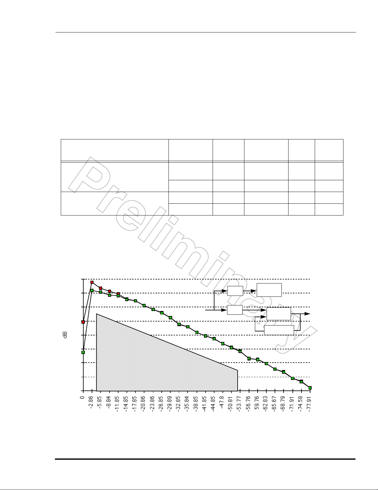
The A/D and D/A performance of the codec section are given in Table 8 with an
example presented in Figure 4.
= -40° to +125°C)
J
Table 8 A/D and D/A Performance of Codec
nc...
I
cale Semiconductor,
Frees
Characteristic
Analog to Digital Section Signal to Nois e
plus Distortion Ratio (S/N+T)
Digital to Analog Sect ion Sign al to Noise
plus Distortion Ratio (S/N+T)
NOTES: 1. 0 dB gain on the A/D and D/A; Co dec clock a t 1.538 MHz with 12 8 decima tion/interpol ation ratio and
tested at 1502 Hz
2. 0 dBm0 corresponds to -3.14 dB below the input saturation level
80
70
60
50
40
30
S/N
S/N+T
Level Min
0 dBm0
(See Note 2)
-50 dBm0 15 20 — dB
0 dB 55 65 — dB
-50 dB 15 20 — dB
13 MHz
55 65 —dB
2 MHz
÷ 6.5
÷ 13
÷13
Typ
(See Note 1)
CODEC
Codec
1 MHz
PLL
PLL
÷(12+1)x4
÷(12+1)*4
Max
COCR=$E400
Unit
52 MHz
20
10
0
S in dB
Signal in dB
Figure 4 Example: S/N and S/N+T Performance for the A/D Section
MOTOROLA DSP56156 Data Sheet 17
For More Information On This Product,
Go to: www.freescale.com
Page 18
Electrical Charac teristics and Timing
Other On-Chip Codec Characteristics
Other On-Chip Codec Characteristics
(V
= 5.0 V dc ± 10%, T
CCA
The analog I/O characteristics of this device are shown in Table 9.
Table 9 Analog I/O Characteristics of On-Chip Codec
Characteristic Min Typ Max Unit
Freescale Semiconductor, Inc.
= -40° to +125°C, CL = 50 pF + 1 TTL Load)
J
nc...
I
cale Semiconductor,
Frees
Codec Master Clock 0.1 2.048 3 MHz
Codec Sampli ng Rate 78 16000 37000 Hz
A/D Section Group Delay ——0.2msec
D/A Section Group Delay — — 0.2 msec
18 DSP56156 Data Sheet MOTOROLA
For More Information On This Product,
Go to: www.freescale.com
Page 19
Freescale Semiconductor, Inc.
DC Electrical Characteristics and Timing
DC Electrical Characteristics
(GND = 0 V dc)
= 5.0 V dc ± 10%, TJ = -40° to +125°C, CL = 50 pF + 1 TTL Load)
(V
CC
The DC electrical characteristics of this device ar e shown in Table 10.
Table 10 DC Electrical Characteristics
Characteristic Symbol Min Typ Max Unit
nc...
I
cale Semiconductor,
Frees
Input High Voltage
except EXTAL, RESET
Input Low Voltage
except EXTAL, MODA, MODB, MODC
Input High Voltage
EXTAL DC coupled
EXTAL AC coupled (See Note 1)
Input Low Voltage
EXTAL DC coupled
EXTAL AC coupled (See Note 1)
Input High Voltage RESET
Input High Voltage MODA, MODB, MODC V
Input Low Voltage MODA, MODB, MODC V
Input Leakage Current
RESET
Three-State (Off-State) Input Current
Output High Voltage (I
Output High Voltage (I
Output Low Voltage (I
Output Low Voltage (IOL = 3.2 mA
, MODA, MODB, MODC, TA, DR, BR
(@2.4 V/0.5 V)
R/W
IOL = 1.6 mA; Open Drain
IOL = 6.7 mA, TXD IOL = 6.7 mA)
HREQ
, MODA, MODB, MODC
V
EXTAL
= -10 µA) V
OH
= -0.4 mA) V
OH
= 10 µA) V
OL
V
IH
V
IL
V
IHC
V
ILC
IHR
IHM
ILM
I
IN
TSI -10 — 10 µA
OHC
OH
OLC
V
OL
2.0 — V
-0.5 — 0.8 V
70% of V
VCC -0.1 — — V
CC
1
-0.5
-0.5
2.5 — V
3.5 — V
-0.5 — 2.0 V
-100
-1
2.4 — — V
——0.1V
——0.4V
—
—
—
—
—
CC
V
CC
V
CC
20% of V
VCC-1
CC
CC
100
1
CC
V
V
V
V
V
µA
µA
Input Capacitance (See Note 2) C
NOTES: 1. When EXTAL is AC coupled, V
2. Input capacitance is periodically sampled and not 100% tested in production.
MOTOROLA DSP56156 Data Sheet 19
For More Information On This Product,
IHC
- V
IN
Š 1 V must be true.
ILC
—10—pF
Go to: www.freescale.com
Page 20
Freescale Semiconductor, Inc.
AC Electrical Characteristics and Timing
Clock Operation Timing
AC Electrical Characteristics
(GND = 0 V dc)
nc...
I
cale Semiconductor,
Frees
The timing waveforms in the AC Electrical Charact eristics ar e tested with a V
0.5 V and a V
minimum of 2.4 V for all pins, except EXTAL, RESET, MODA, MODB and
IH
maximum of
IL
MODC. These five pins are tes ted using the in put levels set forth in the DC Elect rical Charac -
teristics. AC timing spec ifications whi ch are r efer enced to a device i nput signal ar e measured
in production with respect to the 50% point of the respective input signal’s transition. The
DSP56156 output levels are measured with the production test machine V
and VOH refer-
OL
ence levels set at 0.8 V and 2.0 V respectively.
Clock Operation Timing
The system clock to the DSP56156 must be externally supplied to EXTAL as illustrated in
Figure 6.
Table 11 Clock Operation Timing
40 MHz 50 MHz 60 MHz
Num Characteristics Sym
Min Max Min Max Min Max
1 Frequency of Operation (EXTAL) f 0 40 0 50 0 60 MHz
2 Instruction Cycle Time = 2T
3 Wait State Time = T
4 EXTAL Cycle Period T
5 EXTAL Rise Time (See Note 1) — 4 — 3 — 3 ns
6 EXTAL Fall Time (See Note 1) — 4 — 3 — 3 ns
7 EXTAL Width High
48-52% duty cycle
(See Notes 2, 3, 4)
8 EXTAL Width Low
48%-52% duty cycle
(See Notes 2, 3, 4)
C
= 2T — 25 × 20 × 16.6 × ns
C
I
CYC
T
T
50 ×40×33×ns
25 × 20 × 16.6 × ns
C
12 × 9.6 × 8 × ns
H
12 × 9.6 × 8 × ns
L
Unit
NOTES: 1. Rise and fall time may b e relaxed to 12 ns maxi mum if the EXTAL input freq uency is less than o r equal
to 20 MHz. If the EXTAL input frequency is between 20 MHz and 40 MHz, rise and fall time should
meet the specified values in the 40 MHz column (4 ns maximum).
2. The duty cycle may be rela xed to 43-57% i f the EXTAL input frequency is l ess than or equ al to 20 MHz.
If the EXTAL input frequency is between 20 MHz and 40 MHz, the duty cycle should be such that T
and TL meet the specified values in the 40 MH z colum n (12 ns mi nim u m ).
3. T = I
cycle of the external clock input.
4. Duty cycles and EXTAL widths are m easured at the EXTAL inp ut signal midpo int when AC coupled a nd
at VCC/2 when not AC coupled.
20 DSP56156 Data Sheet MOTOROLA
/ 4 is used in the electrical characteristics. The exact length of each T is affected by the duty
CYC
For More Information On This Product,
Go to: www.freescale.com
H
Page 21
EXTAL
Freescale Semiconductor, Inc.
T
7 8
H
4
T
L
6
2
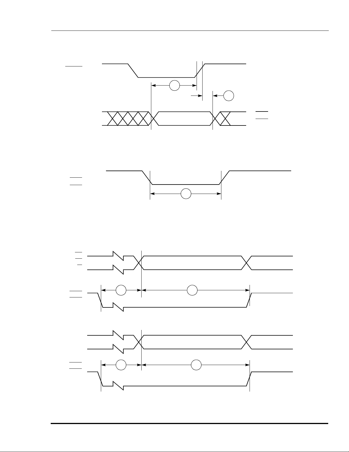
Figure 5 External Clock Timing
Other Clock and PLL Operation Timing
AC Electrical Characteristics and Timing
Clock Operation Timing
PLL
V
IHC
90%
Midpoint
10%
V
ILC
5
nc...
I
cale Semiconductor,
Frees
Clock and PLL timings are listed i n Table 12 and the clocking configurations ar e i llustrated i n
Figure 6.
Table 12 Clock and PLL Timing
Characteristics Min Max Unit
PLL Output frequency 10 Max Fosc
EXTAL Input Clock Amplitude (See Note 2) 1 V
NOTES: 1. Maximum DSP operating frequency. See Table 11.
2. An AC coupling capacitor is required on EXTAL if the levels are out of the normal CMOS level
EXTAL
range (V
100 KΩ
>20% of V
ILC
CC
÷ 1 to ÷ 16
ED3-ED0
or V
IHC
<70% of VCC).
SXFC
PFD
10 nF
XFC
LF
(See Note 1)
0.01 µF
0.1 µF
V
CCS
CC
VCO
MHz
Vpp
GNDS
PLLE=1
Fosc
1000 pF
CLKO
CS1-CS0
÷ 2
÷ 6.5
GSM
PLL
CODEC
÷ 1 to ÷ 16
YD3-YD0
÷ 4
internal phase PH0 at Fosc
PLLE=0
Figure 6 Clocking Configurations
MOTOROLA DSP56156 Data Sheet 21
For More Information On This Product,
Go to: www.freescale.com
Page 22
Freescale Semiconductor, Inc.
AC Electrical Characteristics and Timing
Reset, Stop, Wait, Mode Select, and Interrupt Timing
Reset, Stop, Wait, Mode Select, and Interrupt Timing
(VCC = 5.0 V dc ± 10%, T
cyc = Clock cycle =
J
1
/2 instruction cycle = 2 T cycles
ws = Number of wait states progra mmed into external b us acces s using BCR (WS = 0 - 3 1)
Table 13 Reset, Stop, Wait, Mode Select, and Interrupt Timing
Num Characteristics
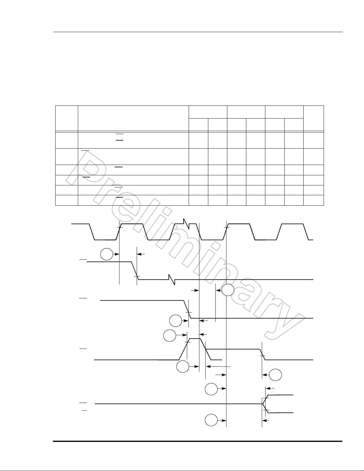
10 RESET
nc...
I
cale Semiconductor,
Control Signals High Impedance
11 Minimum Stabilization Duration
(See Note 1) OMR bit 6=0
12 Asynchronous RESET Deassertion to
First External Address Output
(See Note 7)
13 Synchronous Reset Setup Time from
RESET
CLKO
14 Synchronous Reset Delay Time from
CLKO High to the First External Access
(See Note 7)
15 Mode Select Setup Time
16 Mode Select Hold Time
17 Edge-triggered Interrupt Request Width
18 Delay from IRQA, IRQB Assertion to
External Data Memory Access Out Valid
- Caused by First Interrupt
Frees
- Caused by First Interrupt
Assertion to Address, Data and
OMR bit 6=1
Deassertion to Rising Edge of
Instruction Fetch
Instruction Execution
= -40° to +125°C, CL = 50 pF + 1 TTL Load)
40 MHz 50 MHz 60 MHz
Min Max Mi n Max Min Max
—25—23—21ns
600KT
60T
16T 18T+20 16T 18T+17 16T 18T+15 ns
7 cyc-4 6 cyc-3 5 cyc-2 ns
16T+3 16T+20 16T+ 3 16T+18 16T+3 16T+16 ns
22 — 20 — 18 — ns
0—0—0—ns
13 — 11 — 9 — ns
11T+4
19T+4
—
—
—
—
600KT
60T
11T+4
19T+4
—
—
—
—
600KT
60T
11T+3
19T+3
Unit
—
—
—
—
ns
ns
ns
ns
19 Delay from IRQA, IRQB Assertion to
General Purpose Output Valid Cause d
by the Execution of the First Interrupt
Instruction
20 Delay from External Data Memory
Address Output Valid Caused by First
Interrupt Instruction Execution to Inter-
rupt Request Deassertion for Level Sen-
sitive Fast Interrupts (See Note 2)
22 DSP56156 Data Sheet MOTOROLA
For More Information On This Product,
22T+5
—5T-26
—
+
cyc × ws
22T+4 — 22T+3 — ns
—5T-24
+
cyc × ws
—5T-22
+
cyc × ws
ns
Go to: www.freescale.com
Page 23
Freescale Semiconductor, Inc.
AC Electrical Characteristics and Timing
Reset, Stop, Wait, Mode Select, and Interrupt Timing
(VCC = 5.0 V dc ± 10%, TJ = -40° to +125°C, CL = 50 pF + 1 TTL Load)
Table 13 Reset, Stop, Wait, Mode Select, and Interrupt Timing (continued)
40 MHz 50 MHz 60 MHz
Num Characteristics
Min Max Min Max Min Max
21 Delay from General-Purpose
Output Valid Caused by the
Execution of the First Interrupt Instruction to IRQA,
IRQB
Deassertion for Level
Sensitive Fast Interru pts — If
nc...
I
2nd Interrupt Instruction is:
Single Cycle
(See Note 2)
Two Cycles
—
—
cyc - 29
3 cyc - 29
—
—
cyc - 27
3 cyc - 27
—
—
cyc - 26
3 cyc - 26nsns
Unit
cale Semiconductor,
Frees
22 Synchronous setup time from
, IRQB assertion to
IRQA
Synchronous falling edge of
CLKO (See Notes 5 and 6)
23 Falling Edge of CLKO to First
Interrupt Vector Address Out
Valid after Synchronous
recovery from Wait State
(See Notes 3 and 5)
24 IRQA Width Assertion to
Recover from Stop State
(See Note 4)
25 Delay from IRQA Assertion to
Fetch of first instruction (exiting Stop)
(See Notes 1 and 3)
OMR bit 6=0
OMR bit 6=1
28 Duration for Level Sensitive
IRQA
Assertion to Cause the
Fetch of First IRQA
Instruction (exiting Stop)
(See Notes 1 and 3)
Interrupt
OMR bit 6=0
OMR bit 6=1
14 cyc-3 13 cyc-2 12 cyc-1 ns
27T+3 27T+20 27T+3 27T+18 27T+3 27T+16 ns
15 — 13 — 12 — ns
524303T+4
47T+4
524303T
47T
—
—
—
—
524303T+3
47T+3
524303T
47T
—
—
—
—
524303T+3
47T+3
524303T
47T
—
—
—
—
ns
ns
ns
ns
29 Delay from Level Sensitive
Assertion to First Inter-
IRQA
rupt Vector Address Out
Valid (exiting Stop)
(See Notes 1 and 3)
OMR bit 6=0
OMR bit 6=1
MOTOROLA DSP56156 Data Sheet 23
For More Information On This Product,
524303T+4
47T+4
—
—
524303T+3
47T+3
—
—
524303T+3
47T+3
—
—
ns
ns
Go to: www.freescale.com
Page 24

Freescale Semiconductor, Inc.
AC Electrical Characteristics and Timing
Reset, Stop, Wait, Mode Select, and Interrupt Timing
NOTES: 1. Circuit stabilization delay is required during reset when using an external clock in two cases:
• after po wer-on reset
• when recovering from Stop mode
2. When using fast interrupts, IRQA
apply to prevent multiple interrupt service. To avoid these timing restrictions, the negative edge-triggered mode is recommended when using fast interrupts.
3. The interrupt instruction fetch is visible on the pins only in Mode 3.
4. The minimum is specified for the duration of an edge triggered IRQA interrupt required to recover
from the Stop state. This is not the minimum required so that the IRQA
5. Timing #22 is for all IRQx interrupts while timing #23 is only when exiting the Wait state.
6. Timing #22 triggers off T1 in the normal state and off phi1 when exiting the Wait state.
7. The instruction fetch is visible on the pins only in Mode 2 and Mode 3.
nc...
I
RESET
or IRQB is defined as level-sensitive, then timings 20 and 21
interrupt is accepted.
V
IHR
cale Semiconductor,
Frees
D0-D15
A0-A15
PS/DS
R/W
BS
CLKO
RESET
A0-A15
PS/DS
BS
R/W
11
10
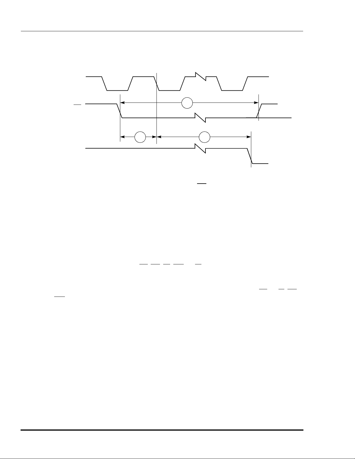
Figure 7 Asynchronous Reset Timing
13
14
12
First Fetch
Figure 8 Synchronous Reset Timing
24 DSP56156 Data Sheet MOTOROLA
For More Information On This Product,
Go to: www.freescale.com
Page 25
RESET
Freescale Semiconductor, Inc.
AC Electrical Characteristics and Timing
Reset, Stop, Wait, Mode Select, and Interrupt Timing
15
16
V
IHR
MODA
MODB
MODC
V
IHM
V
ILM
V
IH
IRQA
V
IL
IRQB
Figure 9 Operating Mode Select Timing
nc...
I
IRQA
IRQB
Figure 10 External Interrupt Timing (Negative Edge-Triggered)
A0-A15
PS/DS
BS
R/W
First Interrupt Instruction Execution
cale Semiconductor,
IRQA
IRQB
17
2018
Frees
a) First Interrupt Instruction Execution
General
Purpose
I/O Pin
IRQA
IRQB
19 21
b) General Purpose I/O
Figure 11 External Level-Sensitive Fast Interrupt Timing
MOTOROLA DSP56156 Data Sheet 25
For More Information On This Product,
Go to: www.freescale.com
Page 26

Freescale Semiconductor, Inc.
AC Electrical Characteristics and Timing
Reset, Stop, Wait, Mode Select, and Interrupt Timing
T0, T2
CLKO
IRQA
IRQB
A0-A15
PD/DS
BS
nc...
I
cale Semiconductor,
R/W
Figure 12 Synchronous Interrupt from Wait State Timing
IRQA
A0-A15
PD/DS
BS
R/W
Figure 13 Recovery from Stop State Using Asynchronous Interrupt Timing
phi0
22
24
T1, T3
phi1
25
23
First Interrupt
Instruction Fetch
First Instruction Fetch
Not IRQA Interrupt Vector
Frees
IRQA
A0-A15
PD/DS
BS
R/W
Figure 14 Recovery from Stop State Using IRQA
26 DSP56156 Data Sheet MOTOROLA
For More Information On This Product,
Go to: www.freescale.com
28
29
First IRQA Interrupt
Instruction Fetch
Interrupt Service
Page 27

Freescale Semiconductor, Inc.
Num Characteristics
30 DR Asserted to CLK high (Setup
Time for Synchronou s Recove ry
from Wait State)
AC Electrical Characteristics and Timing
Reset, Stop, Wait, Mode Select, and Interrupt Timing
Table 14 Wait and Stop Timings
40 MHz 50 MHz 60 MHz
Unit
Min Max Min Max Min Max
10 cyc - 4 9 cyc - 3 8 cyc - 2 ns
nc...
I
cale Semiconductor,
Frees
31 CLK high to DSO (ACK
(Enter Debug Mode) after Synchronous Recovery fr om Wait
State
32 DR
33 DR
to DSO (ACK) Valid
(Enter Debug Mode)
- After Asynchronous Recovery
from Stop State
- After Asynchronous Recovery
from Wait State
Assertion Width
- to Recover from Wait/Stop
without entering debug mode
- to Recover from Wait/Stop
short wake-up and enter
debug mode
- to Recover from Stop
long wake-up and enter
debug mode
DR
(input)
) Valid
18 cyc — 18 cyc — 18 cyc — ns
29 cyc
18 cyc
12
29 cyc
262157
cyc
—
—
10 cyc
—
—
262157
33
33
29 cyc
18 cyc
11
29 cyc
cyc
—
—
10 cyc
—
—
29 cyc
18 cyc
10
29 cyc
262157
cyc
—
—
10 cyc
—
—
ns
ns
ns
ns
ns
32
DSO
(output)
Figure 15 Recovery from Wait State Using DR Pin — Synchronous Timing
MOTOROLA DSP56156 Data Sheet 27
For More Information On This Product,
Go to: www.freescale.com
Page 28
Freescale Semiconductor, Inc.
AC Electrical Characteristics and Timing
Reset, Stop, Wait, Mode Select, and Interrupt Timing
Capacitance Derating
CLKO
(output)
DR
(input)
DSO
nc...
I
(output)
Figure 16 Recovery from Wait/Stop State Using DR Pin — Asynchronous Timing
T0, T2
30
Capacitance Derating
The DSP56156 External Bus T iming Specific ations are designe d and tested at the maximum capacitive load of 50 pF, including stray capacitance. Typically, the drive capability of the External Bus pins (A0-A15, D0-D15, PS/DS
additional capacitance from 50 pF to 250 pF of loading. Port B and C pins derate linearly at 1 ns
per 5 pF of additional capacitance from 50 pF to 250 pF of loading.
cale Semiconductor,
When an internal memory access follows an external memory access, the PS/DS
and WR
strobes remain deasserted and A0-A15 do not change from their previous state.
T1, T3
33
31
, RD, BS, WR, R/W) derates linearly at 1 ns per 12 pF of
, R/W, RD
Frees
28 DSP56156 Data Sheet MOTOROLA
For More Information On This Product,
Go to: www.freescale.com
Page 29

Freescale Semiconductor, Inc.
AC Electrical Characteristics and Timing
External Bus Synchronous Timing
External Bus Synchronous Timing
(VCC = 5.0 V dc ± 10%, TJ = -40° to +125°C, CL = 50 pF + 1 TTL Load)
Table 15 lists external bus synchronous timing. Figure 17 and illustrate the bus timings
with no wait states and two wait states, respectively.
Table 15 External Bus Synchronous Timing
40 MHz 50 MHz 60 MHz
Num Characteristic
nc...
I
34 EXTAL CLK In High to CLKO High 2.4 9 2.4 9 2.4 9 ns
Min Max Min Max Min Max
Unit
cale Semiconductor,
Frees
35 CLKO High to
36 BS
37 CLKO High to WR
38 WR and RD Deasserted High to BS
39 <intentionally blank>
40 CLKO High to BS
41 TA
42 CLKO High to TA
43 CLKO High to D0-D15 Out Valid 1.7 7.1 1.7 7.1 1.7 7.1 ns
44 CLKO High to D0-D15 Out Invalid 2.0 — 2.0 — 2.0 — ns
45 D0-D15 In Valid to CLKO Low (Setup) 6 — 6 — 6 — ns
46 CLKO Low to D0-D15 In Invalid (Hold) 0 — 0 — 0 — ns
47 CLKO Low to WR
48 WR
a. A0-A15 Valid
b. PS/DS
Width Deasserted 18.3 — 13.4 — 9.8 — ns
Asserted Low (2 Successive Bus Cycles)
Valid to CLKO High (Setup) 4.5 — 4.5 — 4.5 — ns
, RD Hold Time from CLKO Low 2.2 — 2.2 — 2.2 — ns
, R/W Valid, BS, RD Asserted
Asserted Low T+3.1 T+12.4 T+3.1 T+12.4 T+3.1 T+12.4 ns
Deasserted 2.6 10.3 2.6 10.3 2.6 10.3 ns
Invalid (Hold) 0 — 0 — 0 — ns
, RD Deasserted — 10 — 10 — 10 ns
4.7
4.7
14.3 15.8 11.8 13.3 10.2 11.8 ns
12
14
4.7
4.7
12
14
4.7
4.7
12
(See Note)
4
ns
ns
49 CLKO High to D0-D15 Three-state 0 6 0 6 0 6 ns
50 CLKO High to D0-D15 Out Active 1.2 4.2 1.2 4.2 1.2 4.2 ns
51 CLKO High to A0-A15, PS/DS
NOTE: 10 ns CL = 25 pF
MOTOROLA DSP56156 Data Sheet 29
For More Information On This Product,
, R/W Invalid 2.8 — 2.8 — 2.8 — ns
Go to: www.freescale.com
Page 30

Freescale Semiconductor, Inc.
AC Electrical Characteristics and Timing
External Bus Synchronous Timing
EXTAL
(Input)
CLKO
(Output)
T0 T1 T2 T3 T0 T1 T2
34
nc...
I
cale Semiconductor,
Frees
A0-A15
PS/DS
R/W
(See Note)
BS
(Output)
WR
(Output)
RD
(Output)
TA
(Input)
D0-D15
(Output)
35
37
35
35
43
50
40
41
47
47
36
42
Data Out
48
48
44
51
41
49
45
D0-D15
(Input)
NOTE: During Read-Modify-Write instructions and internal instructions, the address lines do not change state.
Data In
46
Figure 17 External Bus Synchronous Timing — No Wait States
30 DSP56156 Data Sheet MOTOROLA
For More Information On This Product,
Go to: www.freescale.com
Page 31

EXT AL
(Input)
Freescale Semiconductor, Inc.
T0 T1 T2 Tw T2 Tw T2 T3 T0
AC Electrical Characteristics and Timing
External Bus Synchronous Timing
nc...
I
cale Semiconductor,
Frees
(Output)
A0-A15,
PS/DS
(Outputs)
(Output)
(Output)
(Output)
D0-D15
(Output)
CLKO
, R/W
BS
WR
RD
TA
(Input)
34
35
37
35
35
41
43
50
42
40
Data Out
47
47
41
36
42
48
48
44
51
49
46
45
D0-D15
(Input)
Data In
Figure 18 External Bus Synchronous Timing – Two Wait States
MOTOROLA DSP56156 Data Sheet 31
For More Information On This Product,
Go to: www.freescale.com
Page 32

AC Electrical Characteristics and Timing
External Bus Asynchronous Timing
External Bus Asynchronous Timing
(V
= 5.0 V dc ± 10%, T
CC
cyc = Clock cycle =
WS = Number of Wait States, Determined by BCR Register (WS = 0 to 31)
WT = WS × cyc = 2T × WS
nc...
I
Freescale Semiconductor, Inc.
= -40° to +125°C, CL = 50 pF + 1 TTL Load)
J
1
/2 instruction cycle = 2 T cycles
cale Semiconductor,
Frees
32 DSP56156 Data Sheet MOTOROLA
For More Information On This Product,
Go to: www.freescale.com
Page 33

A0-A15,
PS/DS, R/W
(See Note)
BS
Freescale Semiconductor, Inc.
AC Electrical Characteristics and Timing
60
External Bus Asynchronous Timing
59
nc...
I
cale Semiconductor,
Frees
64
RD
55
53
68 54 66 69
WR
56
58 57
D0-D15
NOTE: During Read-Modify-Write instructions and internal instructions, the address lines do not change state.
Figure 19 External Bus Asynchronous Timing
52
Data Out
62 67
65
63
61
Data In
MOTOROLA DSP56156 Data Sheet 33
For More Information On This Product,
Go to: www.freescale.com
Page 34

AC Electrical Characteristics and Timing
Bus Arbitration Timing — Slave Mode
Bus Arbitration Timing — Slave Mode
(VCC = 5.0 V dc ± 10%, TJ = -40° to +125°C, CL = 50 pF + 1 TTL Load)
cyc = Clock cycle = 1/2 instruction cycle = 2 T cycles
WS = Number of Wait States for external X or P memory, Determined by BCR
Register (WS = 0 to 31)
WT = WS
WX = Number of Wait States for external X memory, Determined by BCR
Register (WS = 0 to 31)
WP = Number of Wait States for external P memory, Determined by BCR
Register (WS = 0 to 31)
nc...
I
Num Characteristics
Freescale Semiconductor, Inc.
× cyc=2T × WS
Table 17 Slave Mode
40/50/60 MHz
Min Max
Unit
cale Semiconductor,
Frees
70 BR Input to CLKO low setup time 0 1 ns
71 Delay from BR
72 CLKO high to BG
73 BG
74 CLKO High to Control Bus High Impedance 2.7 6.5 ns
75 CLKO High to BB Output Deassertion 3.2 7.8 ns
76 CLKO High to BB
77 BR Input Deassertion to (See Note 1)
78 CLKO Low to BG Deassertion (See Note 1)
79 CLKO High to BB
80 CLKO High to BB
81 CLKO High to Address and Control Bus Active 1 3 ns
Output Assertion (See Note 2)
BG
Output Deassertion Duration (See Note 1)
BG Output Deassertion (See Note 5)
CLKO High to BG
CLKO High to BG
Input Assertion to (See Note 1)
(See Note 3)
(See Note 4)
(See Note 5)
Output Assertion 1.9 5.2 ns
(See Note 5)
(See Note 6)
Inpu t 3.3 8.1 ns
(See Note 7)
Deassertion (See Note 5)
Deassertion (See Note 7)
Output Active 1.3 3.6 ns
Output Assertion 2.3 5 ns
5T+1.9
3T+1.9
5T+1.9
NA
T+1.9
5T-0.5
2T-0.5
3T-0.5
4T+2.5
3T+3.2
3T+3.2
2.5
3.2
3.2
9T+4.2
6T+WT+4.2
26T+4T x WX
+2T x WP+4.2
NA
3T+4.2
—
—
—
9T+6.4
8T+7.8
8T+8.0
6.4
7.8
8.0
ns
ns
ns
ns
82 CLKO High to Address and Control Bus Valid 2 4.4 ns
NOTES: 1. With no external access from the DSP56156
2. During external read or write access
3. During external read-modify-write access
4. During Stop mode — external bus is released and BG
5. During Wait mode
6. With external accesses pending by the DSP56156
7. Slave mode, when bus is still busy after bus request has been deasserted
34 DSP56156 Data Sheet MOTOROLA
For More Information On This Product,
Go to: www.freescale.com
is always low
Page 35

Freescale Semiconductor, Inc.
CLKO
(Output)
AC Electrical Characteristics and Timing
Bus Arbitration Timing — Slave Mode
70
BR
(Input)
nc...
I
BG
(Output)
BB
(I/O)
A0-A15
PS/DS
R/W
cale Semiconductor,
D0-D15
71
73
75
72
76
74
Frees
74
Figure 20 Bus Arbitration Timing — Slave Mode — Bus Release
MOTOROLA DSP56156 Data Sheet 35
For More Information On This Product,
Go to: www.freescale.com
Page 36

Freescale Semiconductor, Inc.
AC Electrical Characteristics and Timing
Bus Arbitration Timing — Slave Mode
CLKO
(Output)
70
BR
(Input)
nc...
I
BG
(Output)
BB
(I/O)
A0-A15
PS/DS
R/W
cale Semiconductor,
Figure 21 Bus Arbitration Timing — Slave Mode — Bus Acquisition
77
79
82
81
78
80
Frees
36 DSP56156 Data Sheet MOTOROLA
For More Information On This Product,
Go to: www.freescale.com
Page 37
Freescale Semiconductor, Inc.
AC Electrical Characteristics and Timing
Bus Arbitration Timing — Master Mode
(VCC = 5.0 V dc ± 10%, TJ = -40° to +125°C, CL = 50 pF + 1 TTL Load)
Table 18 Master Mode
40 MHz 50 MHz 60 MHz
Num Characteristic
Min Max Min Max Min Max
Bus Arbitration Timing — Master Mode
Unit
nc...
I
cale Semiconductor,
Frees
85 CLKO High to BR Output Assertion
CLKO High to BR
86 BG
87 CLKO Low to BG
88 BB
89 CLKO Low to BB
90 CLKO High to BB Output Asserted 4.7 12 4.7 12 4.7 12 ns
(Output)
(Output)
(Input)
Input Asserted/ Deasserted to CLKO
Low (Setup)
Input Deasserted to CLKO Low (Setup) 9.2 — 6.5 — 4.5 — ns
CLKO
85
BR
BG
Output Deassertion
Input Invalid (Hold) 0—0—0—ns
Input Deasserted (Hold) 0 — 0 — 0 — ns
86
88
4.7 12 4.7 12 4.7 12 ns
9.2 —6.5—4.5—ns
87
BB
(I/O)
89
82
A0-A15
PS/DS
R/W
Figure 22 Bus Arbitration Timing — Master Mode — Bus Acquisition
MOTOROLA DSP56156 Data Sheet 37
For More Information On This Product,
Go to: www.freescale.com
81
Three-state
90
Page 38

AC Electrical Characteristics and Timing
Bus Arbitration Timing — Master Mode
CLKO
(Output)
BR
(Output)
86
nc...
I
BG
(Input)
Freescale Semiconductor, Inc.
85
87
75
cale Semiconductor,
Frees
BB
(I/O)
A0-A15
PS/DS
R/W
Figure 23 Bus Arbitration Timing — Master Mode — Bus Release
76
74
38 DSP56156 Data Sheet MOTOROLA
For More Information On This Product,
Go to: www.freescale.com
Page 39

Freescale Semiconductor, Inc.
Host Port Timing
AC Electrical Characteristics and Timing
Host Port Timing
nc...
I
cale Semiconductor,
Frees
(VCC = 5.0 V dc ± 10%, T
T = I
cyc = Clock cycle =
t
HSDL
= Host Synchronization Delay Time (See Note 1)
= Host Processor Data Setup Time
t
suh
= -40° to +125°C, C
J
/ 4
CYC
= 50 pF + 1 TTL Load)
L
1
/
instruction cycle= 2 T cycle
2
Active low lines should be “pulled up” in a manner consistent with the AC and DC specifications.
Table 19 Host Port Timing
40 MHz 50 MHz 60 MHz
Num Characteristic
Min Max Min Max Min Max
100 tHSDL Host Synchronous Delay
(See Note 1)
101 HEN
102 HEN
103 Minimum Cycle Time Betw een Two
104 Host Data Input Setup Time b efore
/HACK Assertion Width
• CVR, ICR, ISR Read
• Read
• Write
(See Notes 2, 4)
/HACK Deassertion Width
(See Note 2)
HEN
Assertion for Consecutive
CVR, ICR, ISR Reads
/HACK Deassertion
HEN
T3TT3TT3Tns
2T+36
32+t
suh
32
31 — 29 — 27 — ns
4T+36 — 4T+33 — 4T+30 — ns
5—4—3—ns
—
—
2T+33
29+t
29
suh
—
—
2T+30
26+t
26
suh
—
—
Unit
ns
105 Host Data Input Hold Time after
HEN
/HACK Deassertion
106 HEN/HACK Assertion to Output
Data Active from High Impedance
107 HEN
108 HEN
109 Output Data Hold Time after
MOTOROLA DSP56156 Data Sheet 39
/HACK Assertion to Output
Data Valid
/HACK Deassertion to Output
Data High Impedance
HEN
/HACK Deassertion
For More Information On This Product,
Go to: www.freescale.com
7—6—5—ns
0—0—0—ns
—32—29—26ns
— 20 — 18.5 — 17 ns
5—5—4—ns
Page 40

Freescale Semiconductor, Inc.
AC Electrical Characteristics and Timing
Host Port Timing
Table 19 Host Port Timing (continued)
40 MHz 50 MHz 60 MHz
Num Characteristic
Min Max Min Max Min Max
110 HR/W Low Setup Time before HEN Assertion 6 — 5 — 4 — ns
Unit
111 HR/W
112 HR/W High Setup Time to HEN Assertion 6 — 5 — 4 — ns
113 HR/W
nc...
I
114 HA0-HA2 Setup Time before HEN
115 HA0-HA2 Hold Time after HEN
116 DMA HACK Assertion to HREQ Deassertion
117 DMA HACK
118 Delay from HEN
cale Semiconductor,
119 Delay from HEN
120 Delay from HEN
Frees
Low Hold Time after HEN Deassertion 6 — 5 — 4 — ns
High Hold Time after HEN/HACK
Deassertion
Assertion 9 — 7.5 — 6 — ns
Deassertion 8—7—6—ns
(See Note 3)
Deassertio n to HREQ
Assertion (See Note 3)
for DMA RXL Read
for DMA TXL Write
for All Other Cases
Deassertion to HREQ
Assertion for RXL Read (See Note 3)
Deassertion to HREQ
Assertion for TXL Write (See Note 3)
Assertion to HREQ
Deassertion for RXL Read, TXL Write
(See Note 3)
5—4—3—ns
52T
+37
t
HSDL
+3T+5
t
HSDL
+2T+5
5
t
HSDL
+3T+5
t
HSDL
+2T+5
52T
—
—
—
—t
—t
+37
52T
+36
t
HSDL
3T+5
t
HSDL
+2T+5
5
HSDL
+3T+5
HSDL
+2T+5
52T
—
—
—
—t
—t
+36
42T
t
HSDL
+3T+4
t
HSDL
+2T+4
4
HSDL
+3T+4
HSDL
+2T+4
52T
+35
—
—
—
—ns
—ns
+35
ns
ns
ns
ns
ns
NOTES: 1. “Host Synchronization Del ay (tHS DL)” is th e time perio d requi red for th e DSP56156 to sam ple any
external asynchronous input signal, determine whether it is high or low, and synchronize it to the
internal clock.
2. See Host Port Considerations.
3. HREQ is pulled up by 1 kΩ.
4. Only if two consecutive reads from one of these registers are executed.
40 DSP56156 Data Sheet MOTOROLA
For More Information On This Product,
Go to: www.freescale.com
Page 41

Freescale Semiconductor, Inc.
External
Internal
nc...
I
AC Electrical Characteristics and Timing
Host Port Timing
100100
Figure 24 Host Synchronization Delay
cale Semiconductor,
Frees
HREQ
(Output)
HACK
(Input)
HR/W
(Input)
H0-H7
(Output)
106
112
101
103
109
Data Valid
113
108107
102
Figure 25 Host Interrupt Vector Register (IVR) Read
MOTOROLA DSP56156 Data Sheet 41
For More Information On This Product,
Go to: www.freescale.com
Page 42

Freescale Semiconductor, Inc.
AC Electrical Characteristics and Timing
Host Port Timing
nc...
I
cale Semiconductor,
Frees
HREQ
(Output)
HEN
(Input)
HA0-HA2
(Input)
HR/W
(Input)
H0-H7
(Output)
RXH
Read
101 102
114 115
Address
Valid
112 113
107 108
106
120
103
109
Data
Valid
Figure 26 Host Read Cycle (Non-DMA Mode)
HREQ
(Output)
HEN
(Input)
HA0-HA2
(Input)
TXH
Write
101 102
114 115
Address
Valid
120
103
118
RXL
Read
Address
Valid
119
TXL
Write
Address
Data
Valid
Valid
110 111
HR/W
(Input)
104 105
H0-H7
(Input)
Data
Valid
Data
Valid
Figure 27 Host Write Cycle (Non-DMA Mode)
42 DSP56156 Data Sheet MOTOROLA
For More Information On This Product,
Go to: www.freescale.com
Page 43

Freescale Semiconductor, Inc.
HREQ
(Output)
116 117
AC Electrical Characteristics and Timing
Host Port Timing
nc...
I
cale Semiconductor,
Frees
102
Data
Valid
HACK
(Input)
H0-H7
(Output)
101
RXH
Read
107
106
Figure 28 Host Read Cycle (DMA Mode)
HREQ
(Output)
116 117
101 102
HACK
(Input)
TXH
Write
108
109
RXL
Read
TXL
Write
Data
Valid
104
105
H0-H7
(Input)
Data
Valid
Data
Valid
Figure 29 Host Write Cycle (DMA Mode)
MOTOROLA DSP56156 Data Sheet 43
For More Information On This Product,
Go to: www.freescale.com
Page 44
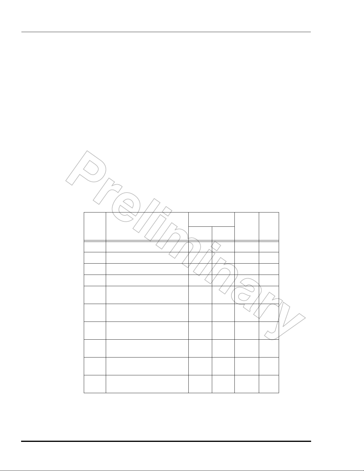
Freescale Semiconductor, Inc.
AC Electrical Characteristics and Timing
SSI Timing
Synchronous Serial Interfaces (SSI) Timing
(VCC = 5.0 V dc ± 10%, TJ = -40° to + 125°C, CL = 50 pF + 1 TTL Load)
T= I
CYC
/ 4
SCK = Serial Clock Pin
FST (T ransmit Frame Sync) = SCx0 Pin
FSR (Receive Frame Sync) = SCx1 Pin
i ck = Internal Clock
x ck = External Clock
i ck a = Internal Clock, Asynchronous Mode (Asynchronous
implies that FSR and FST are two different frame syncs)
i ck s = Internal Clock, Synchronous Mode (Synchronous implies
nc...
I
bl = bit length
that only one frame sync FS is used)
wl = word length
Table 20 Synchronous Serial Interfaces Timing
40/50/60 MHz
Num Characteristic
Min Max
130 Clock Cycle (See Note) 100 ——ns
131 Clock High Period 45 — — ns
132 Clock Low Period 45 — — ns
133 Output Clock Rise/Fall Time — 7 — ns
cale Semiconductor,
134 SCK Rising Edge to FSR Out
(bl) High
135 SCK Rising Edge to FSR Out
(bl) Low
—
—
—
—
32
18
32
15
Case Unit
x ck
i ck a
x ck
i ck a
ns
ns
Frees
NOTE: All the timings for the SSI are given for a non-inverted serial clock polarity (SCKP=0 in CRB) and a non-
inverted frame sync (FSI=0 in CRB). If the polari ty of the clock and/ or the frame sync have been inverte d,
all the timings remain valid by invertin g the clock signal SC K and/or the frame sync FSR/ FST in the tables
and in the figures.
44 DSP56156 Data Sheet MOTOROLA
136 SCK Rising Edge to FSR Out
(wl) High
137 SCK Rising Edge to FSR Out
(wl) Low
138 Data In Setup Time before SCK
Falling Edge
139 Data In Hold Time after SCK
Falling Edge
For More Information On This Product,
Go to: www.freescale.com
—
—
—
—
30
40
25
12
32
15
32
15
—
—
—
—
x ck
i ck a
x ck
i ck a
x ck
i ck
x ck
i ck
ns
ns
ns
ns
Page 45

Freescale Semiconductor, Inc.
nc...
I
AC Electrical Characteristics and Timing
SSI Timing
cale Semiconductor,
Frees
MOTOROLA DSP56156 Data Sheet 45
For More Information On This Product,
Go to: www.freescale.com
Page 46

Freescale Semiconductor, Inc.
AC Electrical Characteristics and Timing
SSI Timing
Table 20 Synchronous Serial Interfaces Timing (continued)
Num Characteristic
40/50/60MHz
Case Unit
Min Max
nc...
I
cale Semiconductor,
Frees
140 FSR Input (bl) High before SCK
141 FSR Input (wl) High before SCK
142 FSR Input Hold Time after SCK
143 Flags Input Setup before SCK
144 Flags Input Hold Time after SCK
145 SCK Rising Edge to FST Out
146 SCK Rising Edge to FST Out
147 SCK Rising Edge to FST Out
148 SCK Rising Edge to FST Out
149 SCK Rising Edge to Data Out
150 SCK Rising Edge to Data Out Valid —
151 SCK Rising Edge to Data Out High
152 FST Input (bl) Setup Time before SCK
153 FST Input (wl) to Data Out Enable from
Falling Edge
Falling Edge
Falling Edge
Falling Edge
Falling Edge
(bl) High
(bl) Low
(wl) High
(wl) Low
Enable from High Impedance
Impedance
Falling Edge
High Impedance
15
15
15
15
15
—
—
—
—
—
—
—
—
—
—
—
—
—
16
—36 —ns
7
7
7
7
7
6
—
—
—
—
—
—
—
—
—
—
33
15
30
15
30
15
33
15
30
12
30
12
30
20
—
—
x ck
i ck a
x ck
i ck a
x ck
i ck a
x ck
i ck
x ck
i ck
x ck
i ck
x ck
i ck
x ck
i ck
x ck
i ck
x ck
i ck
x ck
i ck
x ck
i ck
x ck
i ck
ns
ns
ns
ns
ns
ns
ns
ns
ns
ns
ns
ns
ns
154 FST Input (wl) Setup Time before SCK
155 FST Input Hold Time after SCK
156 Flag Output Valid after SCK
46 DSP56156 Data Sheet MOTOROLA
Falling Edge
Falling Edge
Rising Edge
For More Information On This Product,
8
17
15
4
—
—
—
—
—
—
32
15
x ck
i ck
x ck
i ck
x ck
i ck
ns
ns
ns
Go to: www.freescale.com
Page 47

Freescale Semiconductor, Inc.
AC Electrical Characteristics and Timing
130
SSI Timing
nc...
I
cale Semiconductor,
Frees
133
SCK
(Input/Output)
FSR (Bit)
Out
FSR (Word)
Out
Data In
FSR (Bit)
FSR (Word)
131 132
134
140 142
In
In
135
136 137
138 139
First Bit Last Bit
142141
143 144
Flags In
Figure 30 SSI Receiver Timing
MOTOROLA DSP56156 Data Sheet 47
For More Information On This Product,
Go to: www.freescale.com
Page 48

Freescale Semiconductor, Inc.
AC Electrical Characteristics and Timing
Timer Timin g
130
133
SCK
(Input/Output)
FST (Bit)
Out
nc...
I
FST (Word)
Out
Data Out
FST (Bit)
In
131
145
152
cale Semiconductor,
132
146
147 148
150
149
155
153
154
150
First Bit Last Bit
155
151
Frees
48 DSP56156 Data Sheet MOTOROLA
FST (Word)
In
156
(See Note)
Flags Out
Figure 31 SSI Transmitter Timing
NOTE: In the Network mode, output flag transitions can occur at the start of each time slot within the frame.
In the Normal mode, the output flag state is asserted for the entire frame period.
For More Information On This Product,
Go to: www.freescale.com
Page 49

Freescale Semiconductor, Inc.
AC Electrical Characteristics and Timing
OnCE Port Timing
Timer Timing
(VCC = 5.0 V dc ± 10%, TJ = -40° to +125°C, CL = 50 pF + 1 TTL Load)
Table 21 Timer Timing
40/50/60 MHz
Num Characteristic
Min Max
170 TIN Valid to CLKO Low (Setup time) 6 —ns
171 CLKO Low to TIN Invalid (Hold time) 0 — ns
nc...
I
172 CLKO High to TOUT Asserted 3.5 14 ns
173 CLKO High to TOUT Deasserted 5.1 20.7 ns
Unit
cale Semiconductor,
Frees
174 TIN Period 8T — ns
175 TIN High/Low Period 4T — ns
CLKO
(Output)
170
TIN
(Input)
TOUT
(Output)
172
171
173
Figure 32 Timer Timing
MOTOROLA DSP56156 Data Sheet 49
For More Information On This Product,
Go to: www.freescale.com
Page 50

AC Electrical Characteristics and Timing
OnCE Port Timing
OnCETM Port Timing
(VCC = 5.0 V dc ± 10%, TJ = -40° to +125°C, CL = 50 pF + 1 TTL Load)
Num Characteristic
180 DSCK High to DSO Valid —37ns
nc...
I
181 DSI Valid to DSCK Low (Setup) 5.2 — ns
182 DSCK Low to DSI Invalid (Hold) 0 — ns
Freescale Semiconductor, Inc.
Table 22 OnCE Port Timing
40/50/60 MHz
Min Max
Unit
cale Semiconductor,
Frees
183 DSCK High (See Note 1) 2Tc — ns
184 DSCK Low (See N ote 1) 2Tc — ns
185 DSCK Cycle Time (See Note 1) 4Tc — ns
186 CLKO High to OS0-OS1 Valid 14.5 ns
187 CLKO High to OS0-OS1 Invalid — — ns
188 Last DSCK High to OS0-OS1 (See Note 2)
189 DSO (ACK
190 DSO (ACK
191 DSO (ACK) Width Asserted:
192 Last DSCK High of Read Register to First
193 DSCK High to DSO Invalid (See Note 2) Td+11.2 — ns
194 DR
Last DSCK High to ACK
Last DSCK High to ACK Active (command) (See Note 2)
) Asserted to OS0-OS1 Three-state — 0 ns
) Asserted to First DSCK High 3Tc — ns
• when entering debug mode
• when acknowledging command/data transfer
DSCK High of Next Command
asserted to DSO (ACK) Asserted 11T+19.5 — ns
Active (data) (See Note 2)
10T+Td+14.5
10T+Td+13.5
21T+Td+13.5
3T-2
2Tc+0.5
6Tc — ns
—
—
3T-5
2Tc+3
ns
ns
ns
NOTES: 1. 45%-55% duty cycle
2. Td = DSCK High (Timing #183)
50 DSP56156 Data Sheet MOTOROLA
For More Information On This Product,
Go to: www.freescale.com
Page 51
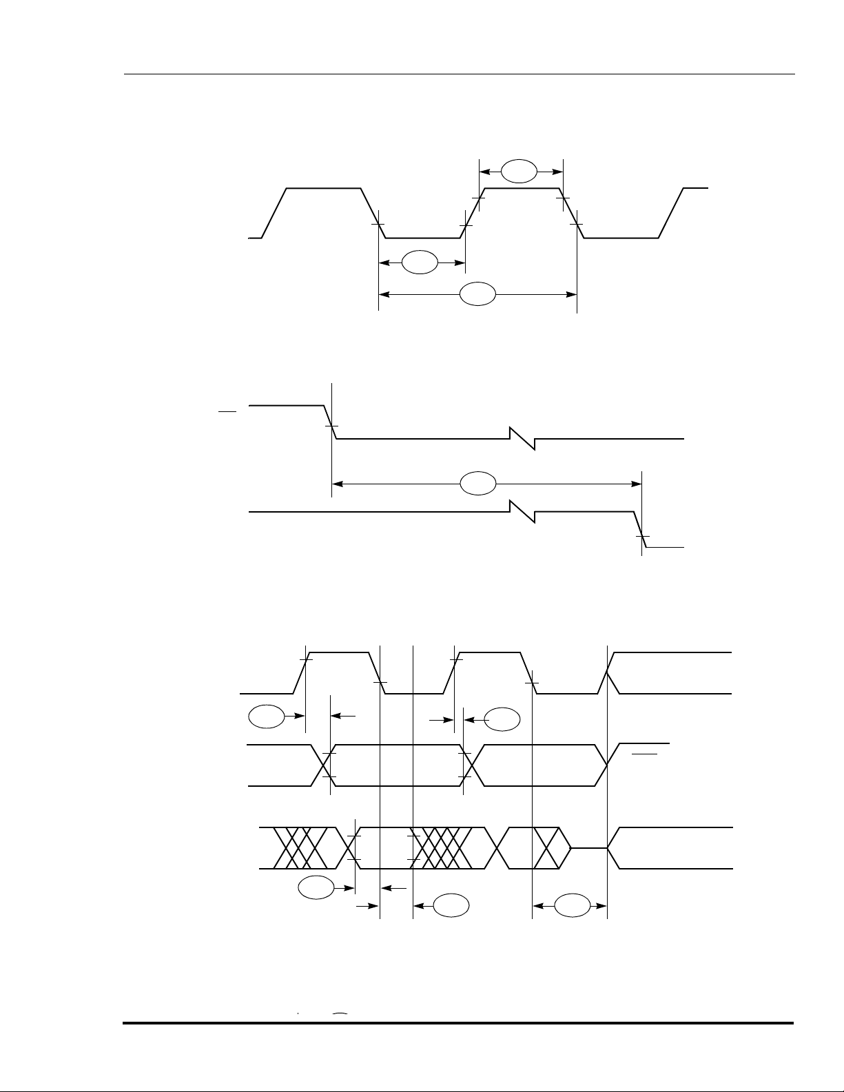
Freescale Semiconductor, Inc.
DSCK
(Input)
nc...
I
DR
(Input)
AC Electrical Characteristics and Timing
OnCE Port Timing
183
184
185
Figure 33 OnCE Port Serial Clock Timing
cale Semiconductor,
Frees
DSO
(Output)
DSCK
(Input)
DSO
(Output)
DSI
(Input)
194
Figure 34 OnCE Port Acknowledge Timing
180
193
(See Note)
(OS1)(Last)
(ACK)
(OS0)
ACK
181
182
NOTE: Three-state, external pull-down resistor
Figure 35 OnCE Port Da ta I/O To Status Timing
MOTOROLA DSP56156 Data Sheet 51
For More Information On This Product,
Go to: www.freescale.com
188
Page 52

Pin-out and Package
Top View
Freescale Semiconductor, Inc.
Pin-out and Package Information
nc...
I
cale Semiconductor,
Frees
GND4
D2
D3
CC3
V
D4
D5
GND5
D6
D7
D8
D9
GND6
D10
D11
CC4
V
D12
D13
GND7
D14
D15
TA
DR
VCCA
SPKP
SPKM
GNDA
VDIV
VREF
D1D0A15
A14
GND3
A13
1
Orientation Mark
A12
A1 1
GNDQ1
CC2
V
A10
GND2A9A8A7A6
(Top View)
29
CCQ1
V
GND1A5A4
CC1
V
A3A2GND0A1A0
MODC
MODB/IRQB
85
57
MODA/IRQA
RESET
STD0/PC0
SRD0/PC1
SCK0/PC2
SC10/PC3
SC00/PC4
TIN/PC10
CC7
V
TOUT/PC11
HA0/PB8
GND10
HA1/PB9
HA2/PB10
/PB11
HR/W
/PB12
HEN
HACK/PB14
HREQ/PB13
H0/PB0
H1/PB1
STD1/PC5
SRD1/PC6
H4/PB4
H3/PB3
H2/PB2
CC6
V
H5/PB5
H6/PB6
BG
MIC
AUX
BIAS
VCCQ0
NOTE: An OVERBAR indicates the signal is asserted when the voltage = ground (active low).
VCC5
WR
BB
BR
RD
GND8
PS/DS
BS
R/W
DSO
DSCK/OS1
DSI/OS0
CLKO
GNDQ0
CCS
V
SXFC
GNDS
EXTAL
SC01/PC9
GND9
SC11/PC8
H7/PB7
SCK1/PC7
Figure 39 T op View of t he DSP56156 1 12-pin Plastic (FC) an d Ceramic (FE) Quad Flat Packages
52 DSP56156 Data Sheet MOTOROLA
For More Information On This Product,
Go to: www.freescale.com
Page 53

Freescale Semiconductor, Inc.
Pin-out and Package
Bottom View
nc...
I
cale Semiconductor,
Frees
MODA/IRQA
RESET
STD0/PC0
SRD0/PC1
SCK0/PC2
SC10/PC3
SC00/PC4
TIN/PC10
CC7
V
TOUT/PC11
HA0/PB8
GND10
HA1/PB9
HA2/PB10
/PB11
HR/W
/PB12
HEN
HACK/PB14
HREQ/PB13
H0/PB0
H1/PB1
STD1/PC5
SRD1/PC6
H4/PB4
H3/PB3
H2/PB2
CC6
V
H5/PB5
H6/PB6
57
MODB/IRQB
MODCA0A1
85H7/PB7
GND0A2A3
CC1
V
A4A5GND1
CCQ1
V
A6A7A8A9GND2
(Bottom View)
CC2
A10
V
GNDQ1
A1 1
A12
Orientation Mark
(on Top side)
A13
GND3
A14
A15D0D1
29
1
GND4
D2
D3
CC3
V
D4
D5
GND5
D6
D7
D8
D9
GND6
D10
D11
CC4
V
D12
D13
GND7
D14
D15
TA
DR
VCCA
SPKP
SPKM
GNDA
VDIV
VREF
BS
PS/DS
RD
GND8
CCS
V
SXFC
GND9
EXTAL
SC11/PC8
SCK1/PC7
NOTE: An OVERBAR indicates the signal is asserted when the voltage = ground (active low).
SC01/PC9
CLKO
GNDS
GNDQ0
DSI/OS0
DSO
DSCK/OS1
R/W
WR
VCC5
BB
BR
BG
VCCQ0
MIC
AUX
BIAS
Figure 40 Bottom View of the DSP56156 112-pin Plastic (FC) and Ceramic (FE) Quad Flat Packages
MOTOROLA DSP56156 Data Sheet 53
For More Information On This Product,
Go to: www.freescale.com
Page 54

Pin-out and Package
General Purpose I/O
Freescale Semiconductor, Inc.
Table 23 DSP56156 General Purpose I/O Pin Identification
112-pin
Package
Pin #
66 H0 PB0
65 H1 PB1
60 H2 PB2
nc...
I
cale Semiconductor,
61 H3 PB3
62 H4 PB4
58 H5 PB5
57 H6 PB6
56 H7 PB7
74 HA0 PB8
72 HA1 PB9
71 HA2 PB10
70 HR/W
69 HEN
67 HREQ
68 HACK
82 STD0 PC0
81 SRD0 PC1
80 SCK0 PC2
79 SC10 PC3
DSP56156
Primary Pin
Function
DSP56156
General
Purpose I/O
ID
PB1 1
PB12
PB13
PB14
Frees
NOTES: 1. In T ables 23, 24, and 25, OVERBAR
2. For more information on power and ground, see Table 26 under Design Considerations.
54 DSP56156 Data Sheet MOTOROLA
78 SC00 PC4
64 STD1 PC5
63 SRD1 PC6
55 SCK1 PC7
54 SC11 PC8
52 SC01 PC9
77 TIN PC10
75 TOUT PC1 1
indicates the signal is asserted when the voltage = ground (active low).
For More Information On This Product,
Go to: www.freescale.com
Page 55

Freescale Semiconductor, Inc.
nc...
I
Pin-out and Package
Pin Number
cale Semiconductor,
Frees
MOTOROLA DSP56156 Data Sheet 55
For More Information On This Product,
Go to: www.freescale.com
Page 56

Pin-out and Package
Signal Name
Table 24 DSP56156 Pin Identificati on by Pin Number
Freescale Semiconductor, Inc.
112-pin
Package
Pin #
nc...
I
cale Semiconductor,
Frees
56 DSP56156 Data Sheet MOTOROLA
Signal Name
1GND4 39RD
2D2 40PS/DS 77 TIN/PC10
3D3 41BS
4V
5 D4 43 DSO 80 SCK0/PC2
6 D5 44 DSCK/OS1 81 SRD0/PC1
7 GND5 45 DSI/OS0 82 STD0/PC0
8D6 46CLKO 83RESET
9D7 47GNDQ0 84MODA/IRQA
10 D8 48 GNDS 85 MODB/IRQB
11 D9 49 SXFC 86 MODC
12 GND6 50 V
13 D10 51 EXTAL 88 A1
14 D11 52 SC01/PC9 89 GND0
15 V
16 D12 54 SC11/PC8 91 A3
17 D13 55 SCK1/PC7 92 V
18 GND7 56 H7/PB7 93 A4
19 D14 57 H6/PB6 94 A5
20 D15 58 H5/PB5 95 GND1
21 TA
22 DR 60 H2/PB2 97 A6
23 V
24 SPKP 62 H4/PB4 99 A8
25 SPKM 63 SRD1/PC6 100 A9
26 GNDA 64 STD1/PC5 101 GND2
27 VDIV 65 H1/PB1 102 A10
28 VREF 66 H0/PB0 103 V
29 MIC 67 HREQ/PB13 104 GNDQ1
30 AUX 68 HACK
31 BIAS 69 HEN
32 BG
33 V
34 BR
35 BB
36 V
37 WR
38 GND8
CC3
CC4
CCA
CCQ0
CC5
112-pin
Package
Pin #
Signal Name
42 R/W 79 SC10/PC3
CCS
53 GND9 90 A2
59 V
61 H3/PB3 98 A7
70 HR/W/PB11 107 A13
71 HA2/PB10 108 GND3
72 HA1/PB9 109 A14
73 GND10 110 A15
74 HA0/PB8 111 D0
75 TOUT/PC11 112 D1
CC6
/PB14 105 A1 1
/PB12 106 A12
112-pin
Package
Pin #
76 V
78 SC00/PC4
87 A0
96 V
For More Information On This Product,
Go to: www.freescale.com
Signal Name
CC7
CC1
CCQ1
CC2
Page 57

Freescale Semiconductor, Inc.
nc...
I
Pin-out and Package
Signal Name
cale Semiconductor,
Frees
MOTOROLA DSP56156 Data Sheet 57
For More Information On This Product,
Go to: www.freescale.com
Page 58

Pin-out and Package
Freescale Semiconductor, Inc.
Table 25 DSP56156 Pin Identification by Signal Name
112-pin
Package
Pin #
nc...
I
100 A9 19 D14 57 H6
102 A10 20 D15 56 H7
105 A11 22 DR
106 A12 44 DSCK 72 HA1
107 A13 45 DSI 71 HA2
109 A14 43 DSO 68 HACK
110 A15 51 EXTAL 69 HEN
cale Semiconductor,
Signal Name
87A0 6D5 47GNDQ0
88 A1 8 D6 104 GNDQ1
90A2 9D7 48GNDS
91 A3 10 D8 66 H0
93 A4 11 D9 65 H1
94 A5 13 D10 60 H2
97 A6 14 D11 61 H3
98 A7 16 D12 62 H4
99 A8 17 D13 58 H5
30 AUX 89 GND0 70 HR/W
35 BB 95 GND1 67 HREQ
32 BG 101 GND2 84 IRQA
31 BIAS 108 GND3 85 IRQB
112-pin
Package
Pin #
Signal Name
112-pin
Package
Pin #
74 HA0
Signal Name
Frees
58 DSP56156 Data Sheet MOTOROLA
34 BR 1 GND4 29 MIC
41 BS
46 CLKO 12 GND6 85 MODB
111 D0 18 GND7 86 MODC
112D1 38GND8 45OS0
2D2 53GND9 44OS1
3D3 73GND10 66PB0
5D4 26GNDA 65PB1
7 GND5 84 MODA
For More Information On This Product,
Go to: www.freescale.com
Page 59

Freescale Semiconductor, Inc.
nc...
I
Pin-out and Package
cale Semiconductor,
Frees
MOTOROLA DSP56156 Data Sheet 59
For More Information On This Product,
Go to: www.freescale.com
Page 60

Pin-out and Package
Freescale Semiconductor, Inc.
Table 25 DSP56156 Pin Identification by Signal Name (continued)
nc...
I
cale Semiconductor,
Frees
112-pin
Package
Pin #
Signal Name
60 PB2 55 PC7 64 STD1
61 PB3 54 PC8 49 SXFC
62 PB4 52 PC9 21 TA
58PB5 77PC10 77TIN
57PB6 75PC11 75TOUT
56 PB7 40 PS/DS
74 PB8 42 R/W 103 V
72 PB9 39 RD 4V
71 PB10 83 RESET 15 V
70 PB11 78 SC00 36 V
69 PB12 52 SC01 59 V
67 PB13 79 SC10 76 V
68 PB14 54 SC11 23 V
82PC0 80SCK0 33V
81PC1 55SCK1 96V
80PC2 25SPKM 50V
79PC3 24SPKP 27VDIV
78 PC4 81 SRD0 28 VREF
64 PC5 63 SRD1 37 WR
112-pin
Package
Pin #
Signal Name
112-pin
Package
Pin #
92 V
Signal Name
CC1
CC2
CC3
CC4
CC5
CC6
CC7
CCA
CCQ0
CCQ1
CCS
63 PC6 82 STD0
60 DSP56156 Data Sheet MOTOROLA
For More Information On This Product,
Go to: www.freescale.com
Page 61

112 CQFP
nc...
I
Freescale Semiconductor, Inc.
Pin-out and Package
cale Semiconductor,
Frees
MOTOROLA DSP56156 Data Sheet 61
For More Information On This Product,
Go to: www.freescale.com
Page 62

Pin-out and Package
Freescale Semiconductor, Inc.
S
S
N
S
N
VIEW Y
θ1
R R1
S
SM
85
R R2
θ2
PIN 1
Identifier
-L-
nc...
I
28
CE
cale Semiconductor,
DATUM
PLANE
0.20 (0.008)
0.20 (0.008)
112
1
29 56
W
-H-
-N-
M
A
108 Place
G
A1
TL-M
T
L-M
Frees
K
C1
VIEW P
NOTES: 1.Dimensioning and tolerancing per ANSI Y14.5M, 1982.
2.Controlling dimension: millimeter.
3.Datum plane -H- is coincident with the bottom of the lead
where the lead exits the ceramic body.
4.Datums -L-, -M- and -N- to be determined at datum plane -H-.
5.Dimensions S and V to be determined at seating plane -T-.
6.Dimensions A and B define maximum ceramic body dimensions
including glass protrusion and mismatch.
84
57
TOP
VIEW
-M-
VIEW P
DATUM
PLANE
-H-
B
S
S
TL-M N
M
0.20 (0.008)
-T-
S
S
TL-M N
V
M
0.20 (0.008)
0.15 (0.006)
SEATING
PLANE
J1
J1
P
-L-, -M-, -N-
VIEW Y
3 Place
F
S S
L-M N
B1
J
0.127 (0.005)
SECTION J1-J1
VIEW ROTATED 90°
D
M
T
112 Place
Case 915-01
MILLIMETERS INCHES
MIN MINMAX MAX
DIM
18.880
A
B
C
D
E
F
G
J
K
P
S
V
W
A1
B1
C1
R1
R2
θ1
θ2
NOTE: BSC = Between Statistical Center
20.400
18.880
20.400
2.740
0.220
2.340
0.220
0.650 BSC 0.0256 BSC
0.130
0.650
0.325 BSC
22.950
23.450
22.950
23.450
0.300
0.200
0.120
1.800 REF
0.200 REF
0.200 REF 0.008 REF
0°
0°
(i.e., typical)
3.450
0.380
3.060
0.330
0.230
0.950
0.600
0.132
8°
8°
0.743
0.743
0.108
0.009
0.092
0.009
0.005
0.026
0.0128 BSC
0.904
0.904
0.012
0.008
0.0047
0.070 REF
0.008 REF
0°
0°
0.0052
PLATING
BASE
METAL
0.803
0.803
0.135
0.015
0.120
0.013
0.009
0.037
0.923
0.923
0.024
8°
8°
Figure 41 DSP56156 112-pin Ceramic Quad Flat Pack (CQFP) Mechanical Information
62 DSP56156 Data Sheet MOTOROLA
For More Information On This Product,
Go to: www.freescale.com
Page 63

Freescale Semiconductor, Inc.
nc...
I
Pin-out and Package
112 TQFP
cale Semiconductor,
Frees
MOTOROLA DSP56156 Data Sheet 63
For More Information On This Product,
Go to: www.freescale.com
Page 64

Pin-out and Package
4x
PIN 1
Identifier
1
-L-
Freescale Semiconductor, Inc.
0.200 (0.008) H
112 85
VIEW Y
L-M N
4x 28 TIPS
0.200 (0.008) T
84
-M-
L-M N
V
B
J1
J1
VIEW Y
4x
P
108x
-L-, -M-, -N-
G
nc...
I
cale Semiconductor,
Frees
C
-H-
NOTES:
B1
V1
28
29
-N-
A1
S1
A
S
C2
0.050 (0.002) S
θ
C1
VIEW AB
1.Dimensioning and tolerancing per ANSI Y14.5M, 1982.
2.Controlling dimension: Millimeter.
3.Datum plane -H- is located at bottom of lead and is coincident with the lead
where the lead exits the plastic body at the bottom of the parting line.
4.Datums -L-, -M- and -N- to be determined at datum plane -H-.
5.Dimensions S and V to be determined at seating plane -T-.
6.Dimensions A and B do not include mold protrusion. Allowable protrusion is
0.25 (0.010) per side. Dimensions A and B do include mold mismatch and are
determin ed at datum plane -H-.
7.Dimension D does not include dambar protrusion. Allowable dambar
protrusion shall not cause the D dimension to exceed 0.43 (0.017).
θ2
θ3
R2
K
E
Y
Z
R1
57
56
TOP
VIEW
VIEW AB
0.100 (0.004)
0.25 (0.010)
GAGE PLANE
θ1
-T-
SEATING
PLANE
J
F
D
0.13 (0.005) T L
(VIEW ROTATED 90° COUNTER CLOCKWISE)
M
SECTION J1-J1
-M
AA
BASE
METAL
M
M
C
Case 987-01
INCHESMILLIMETERS
DIM MIN MAX MIN MAX
A 20.000 BSC 0.790 BSC
A1 10.000 BSC 0.395 BSC
B 20.000 BSC 0.790 BSC
B1 10.000 BSC 0.395 BSC
C 1.400 1.600 0.055 0.063
C1 0.050 0.150 0.002 0.006
C2 1.350 1.450 0.053 0.057
D 0.270 0.370 0.011 0.014
E 0.450 0.750 0.018 0.030
F 0.270 0.330 0.011 0.013
G 0.650 BSC 0.0256 BSC
J 0.115 0.175 0.006 0.007
K 0.500 BSC 0.020 BSC
P 0.325 BSC 0.013 BSC
R1 0.100 0.200 0.004 0.008
R2 0.100 0.200 0.004 0.008
S 22.000 BSC 0.866 BSC
S1 11.000 BSC 0.433 BSC
V 22.000 BSC 0.866 BSC
V1 11.000 BSC 0.433 BSC
Y 0.250 REF 0.010 REF
Z 1.000 REF 0.039 REF
AA 0.115 0.135 0.004 0.005
0°
θ
3°
θ1
11°
θ2
θ3
11°
NOTE: BSC = Between Statistical Center
8°
7°
13°
13°
(i.e., typical)
11°
11°
0°
3°
8°
7°
13°
13°
Figure 42 DSP56156 112-pin Plastic Thin Quad Flat Pack (TQFP) Mechanical Information
64 DSP56156 Data Sheet MOTOROLA
For More Information On This Product,
Go to: www.freescale.com
Page 65

Design Considerations
Heat Dissipation
Power, Ground, and Noise
Design Considerations
Freescale Semiconductor, Inc.
nc...
I
cale Semiconductor,
Frees
Heat Dissipation
The average chip junction temperature, TJ, in
°C, can be obtained from:
= TA + (P
T
J
Where:
= ambient temperature, °C
T
A
= package thermal resistance,
Θ
JA
=P
P
D
P
=I
INT
= power dissipation on input and
P
I/O
For most applications P
be neglected. An appropriate relationship between P
P
and TJ (if P
D
= K/(TJ + 273) (2)
D
Solving equations (1) and (2) for K gives:
K = P
× (TA + 273) + P
D
Where K is a constant pertaining to the particular package. K can be determined from
equation (2) by measuring P
um) for a known T
values of P
ing equations (1) and (2) iteratively for any
value of T
A
package (Θ
ponents, Θ
to heat flow from the s emic onduct o r junction
to the package (case) s urfac e ( Θ
the case to the outside am bi ent ( Θ
terms are related by the equation:
Θ
= ΘJC + Θ
JA
× Θ
D
)(1)
JA
junction-to-ambient, °C/W
+ P
INT
CC
I/O
× V
watts — chip internal
CC
power
output pins — user determined
< P
I/O
is neglected) is:
I/O
. Using this value of K, the
A
and TJ can be obtained by solv-
D
and P
INT
× Θ
D
JA
(at equilibri-
D
I/O
can
(3)
. The total thermal resistance of a
) can be separated into two com-
JA
and ΘCA, representing the barrier
JC
) and from
JC
). These
CA
CA
(4)
ΘJC is device-related and cannot be influ-
enced by the user . However, Θ
is user-de-
CA
pendent and can be minimized by such
thermal management techniques as heat
sinks, ambient air cooling, and thermal convection. Thus, good thermal management on
the part of the us er can significantly reduce
so that ΘJA approximately equals ΘJC.
Θ
CA
Substitution of Θ
for ΘJA in equation (1) will
JC
result in a lower semiconductor junction
temperature. Values for thermal resistance
presented in this document, unless estimated, were derived using the procedure described in Motorola Reliability Report 7843,
“Thermal Resistance Measurement Method
for MC68XX Microcomponent Devices”, a nd
are provided f or design purposes only. Thermal measurements are complex and dependent on procedure and setup. User-derived
values for thermal resistance may differ.
Power, Ground, and
Noise
Each DSP56156 V
with a low-impedance path to +5 volts. Each
DSP56156 GND pin should likewise be provided with a low-impedance path to ground.
The power supply pins drive distinct gr oups
of logic on chip as shown in Table 26.
The V
power supply should be by-
CC
passed to GND ground using at least six
0.01 – 0.1 µF bypass capacitors located either underneath the chip’s socke t or as close
as possible to the four sides of the package.
The capacitor leads and the associated
printed circuit traces connec ting to chip V
and GND should be kept to less than 0.5” per
pin should be provided
CC
CC
60 DSP56156 Data Sheet MOTOROLA
For More Information On This Product,
Go to: www.freescale.com
Page 66

Freescale Semiconductor, Inc.
Design Considerations
Power, Ground, and Noise
capacitor lead. The use of at least a fo ur layer board is recommended, employing two
inner layers as V
and GND planes. All
CC
output pins on this DSP have fast rise and
fall times. Printed Circuit Board (PCB)
trace length should be minimized in order
to minimize undershoot and reflections
caused by these fast output switching
times. This recommendation particularly
applies to the address and data buses as
well as the PS/DS
rupt, and HEN
nc...
I
lengths on the order of 6" are recommended.
Capacitance calculations should consider all
, BS, RD, WR, R/W , inter-
pins. Maximum PCB trace
device loads as well as parasitic capacitances due to PCB traces. Attention to proper
PCB layout and bypassing becomes especially critical in systems with higher capacitive loads because these loads create
higher transient currents in the V
CC
and
GND circuits.
Clock signals should not be run across
many signals and should be kept away
from analog power and ground traces as
well as any analog signals. See Figure 44 for
more details.
Table 26 Power and Ground Connections
Power Ground
Circuitry
Address Bus Buffers
cale Semiconductor,
Data Bus Buffers
Signal
Name
V
CC1
V
CC2
V
CC3
V
CC4
Pin #
92
103
4
15
Signal
Name
GND0
GND1
GND2
GND3
GND4
GND5
GND6
GND7
Pin #
89
95
101
108
1
7
12
18
Frees
Bus Control Buffers
Codec
Digital Peripherals
Internal logic
Phase-Locked Loop (PLL)
MOTOROLA DSP56156 Data Sheet 61
For More Information On This Product,
Go to: www.freescale.com
V
CC5
V
CCA
V
CC6
V
CC7
V
CCQ0
V
CCQ1
V
CCS
36
23
59
76
33
96
50
GND8
GNDA
GND9
GND10
GNDQ0
GNDQ1
GNDS
38
26
53
73
47
104
48
Page 67

Design Considerations
Power Consumption
Power Consumption
Freescale Semiconductor, Inc.
(VCC = 5.0 V dc ± 10%, T
= -40° to +125°C, C
J
= 50 pF + 1 TTL Load)
L
The DC electrical characteristics of this device are shown in Table 27. Power consumption is
application dependant. The data in Table 27 is collected by running the following code using
internal memory after having pr ogrammed all pins of port B and C as input and after having
three-stated the data bus (MC = 0 in OMR) and pulled high:
move #0,r0
move #0,r3
move #$100,r2
nc...
I
loop clr a
cale Semiconductor,
move #$00ff,m0
move x:(r0)+,a ;initial value to accumulator
move a1,a0
rep #30
mac x0,y0,a x:(r3)+,x0 ;mac on typical data
move a,p:(r2) ;store the mac result
move #0,r3
jmp loop
Table 27 DC Electrical Characteristics
Typical
Conditions Symbol
Digital current with Codec and PLL disabled I
Digital current Wait Mode with Codec
and PLL disabled
Digital current Wait Mode with Codec Enabled
and PLL disabled
I
I
CC
CC
CC
40
MHz
91 112 133 mA
12 14 17 mA
92 113 134 mA
MHz
50
60
MHz
Unit
Frees
Stop mode with PLL and CLKO disabled I
Digital current drawn by the PLL when active I
Digital current drawn by CLKO when active I
Analog current with Codec enabled I
Analog current with Codec disabled I
CC
CC
CC
CCA
CCA
— 250 — µA
—1—mA
—3.6—mA
—12—mA
—70—µA
To minimize the power dissipation, all unused digital input pins should be tied inactive to
ground or power; and all unused I/O pi ns should be tied inactive through a 10K¾ resistor to
ground or power . W hen the codec is not used, GNDA should be conn ected to GND; and V
should be connected to V
. Also, all codec pins should be left floating, except VREF which
CC
should still be decoupled.
62 DSP56156 Data Sheet MOTOROLA
For More Information On This Product,
Go to: www.freescale.com
CCA
Page 68

Freescale Semiconductor, Inc.
Design Considerations
Host Port Considerations
nc...
I
cale Semiconductor,
Frees
Host Port
Considerations
Careful synchronization is required when
reading multi-bit r egisters that are written by
another asynchronous syst em. Th is is a common problem when two asynchronous systems are connected. The situation exists in
the host interface. The considerations for
proper operation are discussed below.
Host Programming
Considerations
1. Unsynchronized Reading of
Receive Byte Registers
When reading receive byte registers,
RXH or RXL, the host program should
use interrupts or poll the RXDF flag
which indicates that data is available.
This assures that the data in the receive
byte registers will be stable.
2. Overwriting Transmit Byte Registers
The host program should not write to the
transmit byte registers, TXH or TXL, unless the TXDE bit is set indicating that the
transmit byte registers are empty. This
guarantees that the transmit byte registers will transfer valid data to the HRX
register.
3. Synchronization of Status Bits from
DSP to Host
HC, HREQ, DMA, HF3, HF2, TRDY,
TXDE, and RXDF status bits are set or
cleared from inside the DSP and read by
the host processor (refer to DSP56156 Us-
er’s Manual, I/O Interface section, Host/
DMA Interface Programming Model for
descriptions of these status bits). The
host can read these status bits very quickly without regard to the clock rate used
by the DSP, but the possibility exists that
the state of the bit could be changing during the read operation. This is generally
not a system problem, since the bit will
be read correctly in the next pass of any
host polling routine.
However , if the host asserts HEN
more than timing number 101 (T101),
with a minimum cycle time of timing
number 103 (T103), then these status bits
are guaranteed to be stable. Care must
be exercised when reading status bits
HF3 and HF2 as an encoded pair. If the
DSP changes HF3 and HF2 fr om 00 to 11,
there is a small pr ob ab ili ty th at th e host
could read the bits during the transition
and receive 01 or 10 instead of 11. If the
combination of HF3 and HF2 has significance, the host could read the wrong
combination. Therefore, read the bits
twice and check for consensus.
for
4. Overwriting the Host Vector
The host program should change the
Host Vector register only when the Host
Command bit (HC) is clear. This change
will guarantee that the DSP interrupt
control logic will receive a stable vector.
5. Cancelling a Pending Host Command
Exception
The host processor may elect to clear the
HC bit to cancel the host command exception request at any time before it is
recognized by the DSP. Because the host
does not know exactly when the exception will be recognized (due to exc eption
processing synchronization and pipe line
delays), the DSP may execute the host
command exception after the HC bit is
cleared. For these reasons, the HV bits
must not be changed at the same time
that the HC bit is cleared.
MOTOROLA DSP56156 Data Sheet 63
For More Information On This Product,
Go to: www.freescale.com
Page 69

Design Considerations
T
DSP Programming Considerations
Bus Operatio n
DSP Programming
Considerations
Freescale Semiconductor, Inc.
nc...
I
cale Semiconductor,
Frees
1. Synchronization of Status Bit s
from Host to DSP
DMA, HF1, HF0, and HCP, HTDE,
and HRDF status bits are set or
cleared by the host processor side of
the interface. These bits are individually synchronized to the DSP clock.
(Refer to the DSP56156 User’s Manual,
I/O Interface se c ti on, Host/DMA Interface Programming Model for descriptions of these status bits.)
2. Reading HF0 and HF1 as an
Encoded Pair
Care must be exercised when re ading
status bit s HF0 and HF1 as an encoded pair , i.e., the four combinations 00,
01, 10, and 11 eac h have signific ance.
A very small probability exists that
the DSP will read the status bits synchronized during transition. Therefore, HF0 and HF1 should be read
twice and checked for consensus.
Bus Operation
Figure 43 depicts the operation of the external memory interface with multiple wait states.
T0 T1 T2 Tw T2 Tw T2 Tw T2 T3 T0 T1 T2 Tw T2 Tw T2 Tw T2 T3 T0 T1
CLKO
BS
PS/DS
A0-A15
R/W
WR
RD
D0-D15
Figure 43 Read and Write Bus Operation (3 Wait States)
64 DSP56156 Data Sheet MOTOROLA
For More Information On This Product,
Data in
Go to: www.freescale.com
Data out
Page 70

Freescale Semiconductor, Inc.
Design Considerations
Analog I/O Considerations
Analog I/O Considerations
Figure 44 describes the r ecommended a nalog I/O and power supply conf igurations. The two
analog inputs are electrically identical. When one is not used, it can be left floating. When
used, an AC coupling capacitor is required. The value of the capacitor along with the input
impedance of the pin determine the cut off frequency of a high pass filter. The input imped-
ance of the MIC and AUX varies as a function of the sigma-delta (²ý) modulator master clock.
78 kΩ is a typical value at 2 MHz. An AC capacitor of 1µF defines a high pass filter pole of 2
Hz. A smaller capa citor value will move t his pole higher in frequency.
nc...
I
cale Semiconductor,
Frees
digital V
digital GND
GND
External
GND
1 µF
600 Ω
600 Ω
1 µF
(to microphone)
+
15 µF
GNDA
ð50 nF
CC
0.01 µF
220 µF
Single trace
+
+5 V
External Supply
0.001 µF
0.001 µF
R
Bias
(≤ ±1mA)
0.1 µF
Š10 µF
VREF
5.6 KΩ
VREF
5.6 KΩ
10 KΩ
Š1 KΩ
Single trace
MIC
AUX
Bias
VREF
VDIV
SPKP
SPKM
V
GNDA
15 µF
CCA
54 KΩ
36 KΩ
VC3-VC0
V
CCA
+
GNDA
INS bit
MUX
2.0 V ±10%
(2/5 VCC)
3 POLE
2 ZERO
Low Pass
Filter (LPF)
GNDA
0.1 µF
Analog Decoupling
near DSP
-6 dB
6 dB
17 dB
MGS1-0 bits
Σ∆
modulator
+5 dB
Figure 44 Recommended Analog I/O Configuration
MOTOROLA DSP56156 Data Sheet 65
For More Information On This Product,
Go to: www.freescale.com
Page 71

Design Considerations
Analog I/O Considerations
Figure 45 shows three possib le single-ended output configurations. Configuration (a) is highly
recommended. For configurations (b) and (c), an AC coupling capacitor is required since the
load resistor is tied to GNDA.
GNDA
nc...
I
V
CCA
47 K¾
+
-
VREF
47 K¾
Freescale Semiconductor, Inc.
47 K¾
47 K¾
(a)
SPKP
SPKM
0 < C ð 100 nF
SPKP
Š 500 Ω
NC
SPKM
(b) (c)
0 < C ð 100 nF
0 < C ð 100 nF
Š 500 Ω
SPKP
Š 500 Ω
SPKM
cale Semiconductor,
Frees
Figure 45 Single-ended Output Configurations
Figure 46 shows a recommended layout for power and ground planes.
84 57
56 29
112 85
128
Digital Ground and
Power planes
Analog Ground and
Power planes
Figure 46 Ground and Power planes
66 DSP56156 Data Sheet MOTOROLA
For More Information On This Product,
Go to: www.freescale.com
Page 72

Freescale Semiconductor, Inc.
A four level board is recommended. The top layer (directly under the parts) and the bottom
layer should be interconnect layers. The two center layers should be power and ground.
Ground and power planes should be completely separated. The digital and analog power/
ground planes should not overlap. All codec pins should be over the analog planes. The analog planes should not encompass any digital pins. All codec signal traces should be over the
analog pl anes.
Figure 47 shows that 0.1 µF bypass caps should be located as close to the pins being bypassed
as possible. The ground side of these caps should be connected as close as possibl e to the V
pin. The ground side of the bypass cap should be connected to the V
nc...
I
Design Considerations
Analog I/O Considerations
pin by short traces.
CCA
CCA
cale Semiconductor,
Frees
BIAS
AUX
SPKP
GNDA
Figure 47 Suggested Top Layer Bypassing
The pins with 0.1 µF bypass caps are VREF and GNDA. The la r ges t size practi cal bypass
caps should also be added for each of these pins as well as for the VDIV pin; 10 µF bypass
caps should be considered a minimum value for the larger caps (65 µF on VDIV may be
used). These caps sho uld be near the pa ckage but do not have to be right next t o the pins.
SPKM
0.1 µF
25 µF
CCA
V
VDIV
65 µF
MIC
VREF
0.1 µF
29
28
Š10 µF
10 kΩ
The DAC outputs (SPKP and SPKM) should be run right next to each other as shown on Figure 48.
MOTOROLA DSP56156 Data Sheet 67
For More Information On This Product,
Go to: www.freescale.com
Page 73

Design Considerations
Analog I/O Considerations
Freescale Semiconductor, Inc.
BIAS
AUX
0.25 µF
MIC
VREF
28
29
1nF
5.6 kΩ
47 kΩ
CCA
V
47 kΩ
SPKP
GNDA
nc...
I
47 kΩ
SPKM
VDIV
MIC IN
Copper Fill of unused board space
should be connected to the analog ground plane.
47 kΩ
SPK OUT
cale Semiconductor,
Figure 48 Suggested Bottom Layer Routing
Frees
The output should be used differentially if at all possible. Analog signal traces should be
shielded by running traces connected to analog ground next to them. Unused board area on
both interconnect levels should be copper filled and connected to ana log gr ound. The copper
fill is only shown on this page for clarity and simplicity. The ADC input anti-aliasing should
be done with respect to VREF.
Figure 49 presents four options for good power supply connections.
68 DSP56156 Data Sheet MOTOROLA
For More Information On This Product,
Go to: www.freescale.com
Page 74

SPKP
GNDA
Freescale Semiconductor, Inc.
CCA
V
SPKM
BIAS
AUX
MIC
VDIV
VREF
28
29
GNDA
SPKP
SPKM
10Ω
CCA
V
Design Considerations
Analog I/O Considerations
BIAS
AUX
MIC
29
VDIV
VREF
28
nc...
I
cale Semiconductor,
Frees
Ideal Choice — Two separate power supplies .
Ground planes connected with a single trace as
close as possible to the V
SPKP
GNDA
SPKM
Voltage
Regulator
pin on the codec.
CCA
10Ω
BIAS
AUX
MIC
CCA
VDIV
VREF
V
28
29
Voltage
Regulator
Second Choice — One power supply.
Two regulators, one for the digital supply, one for
the analog supply. Ground planes connected with
a 10 ¾ resistor as close as possible to the V
pin on the codec.
SPKP
GNDA
Voltage
Regulator
10Ω
CCA
VDIV
V
SPKM
BIAS
AUX
MIC
VREF
28
CCA
29
Third Choice — One power supply.
One regulator for the analog supply. Digital supplies driven directly by voltage source. Ground
planes connected with a 10 ¾ resistor as close as
possible to the V
MOTOROLA DSP56156 Data Sheet 69
pin on the codec.
CCA
Figure 49 Four Possible Power Supply Connections
For More Information On This Product,
Go to: www.freescale.com
Fourth Choice — One power supply. Ground
planes connected at source. Ground planes
connected with a 10 ¾ resistor as close as possible to the V
pin on the codec.
CCA
Page 75
Ordering Information
Ordering Information
Table 28 lists information for ordering parts.
Freescale Semiconductor, Inc.
Table 28 DSP56156 Ordering Information
Supply
Voltage
5 V
nc...
I
5 V Plastic Thin Quad
Package Type Pin Count
Ceramic Quad Flat
Pack (CQFP) 112
Flat Pack (TQFP) 112
cale Semiconductor,
Frequency
(MHz)
40 DSP56156FE40
60 DSP56156FE60
40 DSP56156FV40
60 DSP56156FV60
Order Number
Frees
70 DSP56156 Data Sheet MOTOROLA
For More Information On This Product,
Go to: www.freescale.com
Page 76

Freescale Semiconductor, Inc.
nc...
I
cale Semiconductor,
Frees
Motorola reserves the right to make changes without further notice to any products herein to improve reliability, function or design. Motorola does not assume
any liability arising out of the application or use of any product or circuit described herein; neither does it convey any license under its patent rights nor the rights
of others. Motoro la pr odu cts a re not des ig ne d, in ten ded , or au tho ri zed for use as com pon en ts i n sy stem s int end ed for surgical implant into the body, or other
applications intended to support or sustain life, or for any other application in which the failure of the Motorola product could create a situation where pe r sonal
injury or death may occu r. Should Buyer pu rchase or use Mo torol a pro ducts fo r any su ch unint ended or una uthor ized app licati on, Buyer shall inde mnify and
hold Motorola and its officers, employees, subsidiaries, affiliates, and distributors harmless against all claims, costs, damages, and expenses, and reasonable
attorney fees arising out of, directly or indirectly, any claim of personal injury or death associated with such unintended or unauthorized use, even if such claim
alleges that Motorola was negligent regarding the design or manufacture of the part. Motorola and M are registered trademarks of Motorola, Inc. Motorola, Inc.
is an Equal Opportunity/Affirmative Action Employer.
Literature Distribution Centers:
USA: Motorola Literature Distribution; P.O. Box 20912; Phoenix, Arizona 85036.
EUROPE: Motorola Ltd.; European Literature Center; 88 Tanners Drive, Blakelands, Milton Keynes, MK14 5BP, England.
JAPAN: Nippon Motorola Ltd.; 4-32-1, Nishi-Gotanda, Shinagawa-ku, Tokyo 141 Japan.
ASIA-P ACIFIC: Motorola Semiconduct ors H.K. Ltd.; Silicon Harbor Center , No. 2 Dai King Street, Tai Po Industrial Estate, T ai Po, N.T.,
Hong Kong.
MOTOROLA
For More Information On This Product,
Go to: www.freescale.com
 Loading...