

Page 1

DSP56012UM/D
Rev. 0
Published 11/98
DSP56012
24-Bit Digital Signal Processor
User’s Manual
Motorola, Incorporated
Semiconductor Products Sector
DSP Division
6501 William Cannon Drive West
Austin, TX 78735-8598
Page 2

DSP56012UM/D
Rev. 0
Published 11/98
This document (and other documents) can be viewed on the World Wide
Web at http://www.motorola-dsp.com.
This manual is one of a set of three documents. You need the following
manuals to have complete product information: Family Manual, User’s
Manual, and Technical Data.
OnCE
is a trademark of Motorola, Inc.
MOTOROLA INC., 1998
Order this document by DSP56012UM/AD
Motorola reserves the right to make changes without further notice to any products
herein. Motorola makes no warranty, representation or guarantee regarding the
suitability of its products for any particular purpose, nor does Motorola assume any
liability arising out of the application or use of any product or circuit, and specifically
disclaims any and all liability, including without limitation consequential or
incidental damages. “typical” parameters which may be provided in Motorola data
sheets and/or specifications can and do vary in different applications and actual
performance may vary over time. All operating parameters, including “Typicals”
must be validated for each customer application by customer’s technical experts.
Motorola does not convey any license under its patent rights nor the rights of others.
Motorola products are not designed, intended, or authorized for use as components
in systems intended for surgical implant into the body, or other applications
intended to support life, or for any other application in which the failure of the
Motorola product could create a situation where personal injury or death may occur.
Should Buyer purchase or use Motorola products for any such unintended or
unauthorized application, Buyer shall indemnify and hold Motorola and its officers,
employees, subsidiaries, affiliates, and distributors harmless against all claims, costs,
damages, and expenses, and reasonable attorney fees arising out of, directly or
indirectly, any claim of personal injury or death associated with such unintended or
unauthorized use, even if such claim alleges that Motorola was negligent regarding
the design or manufacture of the part. Motorola and are registered trademarks of
Motorola, Inc. Motorola, Inc. is an Equal Opportunity/Affirmative Action Employer.
Page 3

Table of Contents
1.1 INTRODUCTION. . . . . . . . . . . . . . . . . . . . . . . . . . . . . . . . . . 1-3
1.1.1 Manual Organization. . . . . . . . . . . . . . . . . . . . . . . . . . . . . 1-4
1.1.2 Manual Conventions. . . . . . . . . . . . . . . . . . . . . . . . . . . . . 1-5
1.2 DSP56012 FEATURES. . . . . . . . . . . . . . . . . . . . . . . . . . . . . 1-6
1.3 DSP56012 ARCHITECTURAL OVERVIEW . . . . . . . . . . . . . 1-8
1.3.1 Peripheral Modules. . . . . . . . . . . . . . . . . . . . . . . . . . . . . 1-10
1.3.2 DSP Core Processor . . . . . . . . . . . . . . . . . . . . . . . . . . . 1-10
1.3.2.1 Data Arithmetic and Logic Unit (Data ALU) . . . . . . . . 1-11
1.3.2.2 Address Generation Unit (AGU). . . . . . . . . . . . . . . . . 1-11
1.3.2.3 Program Control Unit . . . . . . . . . . . . . . . . . . . . . . . . . 1-12
1.3.2.4 Data Buses. . . . . . . . . . . . . . . . . . . . . . . . . . . . . . . . . 1-12
1.3.2.5 Address Buses. . . . . . . . . . . . . . . . . . . . . . . . . . . . . . 1-12
1.3.2.6 Phase Lock Loop (PLL) . . . . . . . . . . . . . . . . . . . . . . . 1-12
1.3.2.7 On-Chip Emulation (OnCE) Port . . . . . . . . . . . . . . . . 1-13
1.3.3 Memories . . . . . . . . . . . . . . . . . . . . . . . . . . . . . . . . . . . . 1-13
1.3.3.1 Program Memory . . . . . . . . . . . . . . . . . . . . . . . . . . . . 1-13
1.3.3.2 X Data Memory . . . . . . . . . . . . . . . . . . . . . . . . . . . . . 1-15
1.3.3.3 Y Data Memory . . . . . . . . . . . . . . . . . . . . . . . . . . . . . 1-15
1.3.3.4 On-Chip Memory Configuration Bits . . . . . . . . . . . . . 1-15
1.3.3.5 Memory Configuration Bits. . . . . . . . . . . . . . . . . . . . . 1-16
1.3.3.6 External Memory . . . . . . . . . . . . . . . . . . . . . . . . . . . . 1-16
1.3.3.7 Bootstrap ROM . . . . . . . . . . . . . . . . . . . . . . . . . . . . . 1-16
1.3.3.8 Reserved Memory Spaces. . . . . . . . . . . . . . . . . . . . . 1-16
1.3.4 Input/Output . . . . . . . . . . . . . . . . . . . . . . . . . . . . . . . . . . 1-16
1.3.4.1 Parallel Host Interface (HI). . . . . . . . . . . . . . . . . . . . . 1-18
1.3.4.2 Serial Host Interface (SHI). . . . . . . . . . . . . . . . . . . . . 1-18
1.3.4.3 Serial Audio Interface (SAI) . . . . . . . . . . . . . . . . . . . . 1-19
1.3.4.4 General Purpose I/O . . . . . . . . . . . . . . . . . . . . . . . . . 1-19
1.3.4.5 Digital Audio Transmitter (DAX). . . . . . . . . . . . . . . . . 1-19
2.1 SIGNAL GROUPINGS . . . . . . . . . . . . . . . . . . . . . . . . . . . . . 2-3
2.2 POWER. . . . . . . . . . . . . . . . . . . . . . . . . . . . . . . . . . . . . . . . . 2-5
2.3 GROUND . . . . . . . . . . . . . . . . . . . . . . . . . . . . . . . . . . . . . . . 2-6
2.4 PHASE LOCK LOOP (PLL). . . . . . . . . . . . . . . . . . . . . . . . . . 2-7
2.5 INTERRUPT AND MODE CONTROL. . . . . . . . . . . . . . . . . . 2-8
Motorola iii
Page 4

2.6 HOST INTERFACE (HI) . . . . . . . . . . . . . . . . . . . . . . . . . . . 2-10
2.7 SERIAL HOST INTERFACE (SHI) . . . . . . . . . . . . . . . . . . . 2-13
2.8 SERIAL AUDIO INTERFACE (SAI) . . . . . . . . . . . . . . . . . . 2-16
2.8.1 SAI Receive Section. . . . . . . . . . . . . . . . . . . . . . . . . . . . 2-16
2.8.2 SAI Transmit Section . . . . . . . . . . . . . . . . . . . . . . . . . . . 2-17
2.9 GENERAL PURPOSE INPUT/OUTPUT (GPIO) . . . . . . . . 2-18
2.10 DIGITAL AUDIO INTERFACE (DAX) . . . . . . . . . . . . . . . . . 2-18
2.11 ONCE PORT. . . . . . . . . . . . . . . . . . . . . . . . . . . . . . . . . . . . 2-19
3.1 INTRODUCTION. . . . . . . . . . . . . . . . . . . . . . . . . . . . . . . . . . 3-3
3.2 DSP56012 DATA AND PROGRAM MEMORY. . . . . . . . . . . 3-3
3.2.1 X and Y Data ROM. . . . . . . . . . . . . . . . . . . . . . . . . . . . . . 3-4
3.2.2 Bootstrap ROM. . . . . . . . . . . . . . . . . . . . . . . . . . . . . . . . . 3-4
3.3 DSP56012 DATA AND PROGRAM MEMORY MAPS . . . . . 3-4
3.3.1 Reserved Memory Spaces. . . . . . . . . . . . . . . . . . . . . . . . 3-5
3.3.2 Dynamic Switch of Memory Configurations . . . . . . . . . . . 3-8
3.3.3 Internal I/O Memory Map . . . . . . . . . . . . . . . . . . . . . . . . 3-10
3.4 OPERATING MODE REGISTER (OMR) . . . . . . . . . . . . . . 3-12
3.4.1 DSP Operating Mode (MC, MB, MA)—Bits 4, 1, and 0 . 3-12
3.4.2 Program RAM Enable A and Program RAM Enable B (PEA and
PEB)—Bits 2 and 33-12
3.4.3 Stop Delay (SD)—Bit 6. . . . . . . . . . . . . . . . . . . . . . . . . . 3-12
3.5 OPERATING MODES. . . . . . . . . . . . . . . . . . . . . . . . . . . . . 3-13
3.6 INTERRUPT PRIORITY REGISTER . . . . . . . . . . . . . . . . . 3-15
3.7 PHASE LOCK LOOP (PLL) CONFIGURATION. . . . . . . . . 3-19
3.8 OPERATION ON HARDWARE RESET . . . . . . . . . . . . . . . 3-20
4.1 INTRODUCTION. . . . . . . . . . . . . . . . . . . . . . . . . . . . . . . . . . 4-3
4.2 PORT B CONFIGURATION . . . . . . . . . . . . . . . . . . . . . . . . . 4-3
4.2.1 Port B Control (PBC) Register . . . . . . . . . . . . . . . . . . . . . 4-6
4.2.2 Port B Data Direction Register (PBDDR) . . . . . . . . . . . . . 4-7
4.2.3 Port B Data (PBD) Register . . . . . . . . . . . . . . . . . . . . . . . 4-7
4.3 PROGRAMMING THE GPIO . . . . . . . . . . . . . . . . . . . . . . . . 4-8
4.4 HOST INTERFACE (HI) . . . . . . . . . . . . . . . . . . . . . . . . . . . . 4-9
4.4.1 HI Features. . . . . . . . . . . . . . . . . . . . . . . . . . . . . . . . . . . 4-10
4.4.2 HI Block Diagram . . . . . . . . . . . . . . . . . . . . . . . . . . . . . . 4-11
4.4.3 HI—DSP Viewpoint . . . . . . . . . . . . . . . . . . . . . . . . . . . . 4-12
4.4.4 Programming Model—DSP Viewpoint . . . . . . . . . . . . . . 4-13
4.4.4.1 HI Control Register (HCR). . . . . . . . . . . . . . . . . . . . . 4-14
4.4.4.1.1 HCR HI Receive Interrupt Enable (HRIE)—Bit 0 . 4-15
iv Motorola
Page 5

4.4.4.1.2 HCR HI Transmit Interrupt Enable (HTIE)—Bit 1 . 4-15
4.4.4.1.3 HCR HI Command Interrupt Enable (HCIE)—Bit 2 4-15
4.4.4.1.4 HCR HI Flag 2 (HF2)—Bit 3 . . . . . . . . . . . . . . . . . 4-15
4.4.4.1.5 HCR HI Flag 3 (HF3)—Bit 4 . . . . . . . . . . . . . . . . . 4-15
4.4.4.1.6 HCR Reserved—Bits 5, 6, and 7. . . . . . . . . . . . . . 4-16
4.4.4.2 HI Status Register (HSR). . . . . . . . . . . . . . . . . . . . . . 4-16
4.4.4.2.1 HSR HI Receive Data Full (HRDF)—Bit 0. . . . . . . 4-16
4.4.4.2.2 HSR HI Transmit Data Empty (HTDE)—Bit 1 . . . . 4-16
4.4.4.2.3 HSR HI Command Pending (HCP)—Bit 2. . . . . . . 4-17
4.4.4.2.4 HSR HI Flag 0 (HF0)—Bit 3 . . . . . . . . . . . . . . . . . 4-17
4.4.4.2.5 HSR HI Flag 1 (HF1)—Bit 4 . . . . . . . . . . . . . . . . . 4-17
4.4.4.2.6 HSR Reserved—Bits 5 and 6 . . . . . . . . . . . . . . . . 4-18
4.4.4.2.7 HSR DMA Status (DMA)—Bit 7 . . . . . . . . . . . . . . 4-18
4.4.4.3 HI Receive Data Register (HORX). . . . . . . . . . . . . . . 4-18
4.4.4.4 HI Transmit Data Register (HOTX) . . . . . . . . . . . . . . 4-19
4.4.4.5 Register Contents After Reset. . . . . . . . . . . . . . . . . . 4-19
4.4.4.6 DSP Interrupts . . . . . . . . . . . . . . . . . . . . . . . . . . . . . . 4-20
4.4.4.7 HI Usage Considerations—DSP Side . . . . . . . . . . . . 4-21
4.4.5 HI—Host Processor Viewpoint. . . . . . . . . . . . . . . . . . . . 4-21
4.4.5.1 Programming Model—Host Processor Viewpoint . . . 4-21
4.4.5.2 Host Command . . . . . . . . . . . . . . . . . . . . . . . . . . . . . 4-22
4.4.5.3 Interrupt Control Register (ICR). . . . . . . . . . . . . . . . . 4-24
4.4.5.3.1 ICR Receive Request Enable (RREQ)—Bit 0. . . . 4-24
4.4.5.3.2 ICR Transmit Request Enable (TREQ)—Bit 1 . . . 4-24
4.4.5.3.3 ICR Reserved—Bit 2. . . . . . . . . . . . . . . . . . . . . . . 4-25
4.4.5.3.4 ICR HI Flag 0 (HF0)—Bit 3 . . . . . . . . . . . . . . . . . . 4-25
4.4.5.3.5 ICR HI Flag 1 (HF1)—Bit 4 . . . . . . . . . . . . . . . . . . 4-26
4.4.5.3.6 ICR HI Mode Control (HM1 and HM0)—Bits 5 and 64-26
4.4.5.3.7 ICR Initialize Bit (INIT)—Bit 7 . . . . . . . . . . . . . . . . 4-27
4.4.5.4 HI Initialization . . . . . . . . . . . . . . . . . . . . . . . . . . . . . . 4-27
4.4.5.5 Command Vector Register (CVR) . . . . . . . . . . . . . . . 4-29
4.4.5.5.1 CVR HI Vector (HV)—Bits 0–5 . . . . . . . . . . . . . . . 4-29
4.4.5.5.2 CVR Reserved—Bit 6 . . . . . . . . . . . . . . . . . . . . . . 4-30
4.4.5.5.3 CVR Host Command (HC)—Bit 7 . . . . . . . . . . . . . 4-30
4.4.5.6 Interrupt Status Register (ISR). . . . . . . . . . . . . . . . . . 4-30
4.4.5.6.1 ISR Receive Data Register Full (RXDF)—Bit 0. . . 4-30
4.4.5.6.2 ISR Transmit Data Register Empty (TXDE)—Bit 1 4-31
4.4.5.6.3 ISR Transmitter Ready (TRDY)—Bit 2 . . . . . . . . . 4-31
Motorola v
Page 6

4.4.5.6.4 ISR HI Flag 2 (HF2)—Bit 3 (read only) . . . . . . . . . 4-31
4.4.5.6.5 ISR HI Flag 3 (HF3)—Bit 4 (read only) . . . . . . . . . 4-31
4.4.5.6.6 ISR Reserved—Bit 5. . . . . . . . . . . . . . . . . . . . . . . 4-31
4.4.5.6.7 ISR DMA Status (DMA)—Bit 6 . . . . . . . . . . . . . . . 4-32
4.4.5.6.8 ISR Host Request (HOREQ)—Bit 7 . . . . . . . . . . . 4-32
4.4.5.7 Interrupt Vector Register (IVR) . . . . . . . . . . . . . . . . . 4-32
4.4.5.8 Receive Byte Registers (RXH, RXM, RXL) . . . . . . . . 4-32
4.4.5.9 Transmit Byte Registers (TXH, TXM, TXL) . . . . . . . . 4-33
4.4.5.10 Registers After Reset. . . . . . . . . . . . . . . . . . . . . . . . . 4-33
4.4.6 HI Signals. . . . . . . . . . . . . . . . . . . . . . . . . . . . . . . . . . . . 4-35
4.4.6.1 HI Data Bus (H0–H7). . . . . . . . . . . . . . . . . . . . . . . . . 4-35
4.4.6.2 HI Address (HOA2–HOA0) . . . . . . . . . . . . . . . . . . . . 4-35
4.4.6.3 HI Read/Write (HR/W) . . . . . . . . . . . . . . . . . . . . . . . . 4-35
4.4.6.4 HI Enable (HEN) . . . . . . . . . . . . . . . . . . . . . . . . . . . . 4-35
4.4.6.5 Host Request (HOREQ). . . . . . . . . . . . . . . . . . . . . . . 4-35
4.4.6.6 Host Acknowledge (HACK) . . . . . . . . . . . . . . . . . . . . 4-36
4.4.7 Servicing the HI . . . . . . . . . . . . . . . . . . . . . . . . . . . . . . . 4-37
4.4.7.1 HI—Host Processor Data Transfer . . . . . . . . . . . . . . 4-37
4.4.7.2 Host Interrupts using Host Request (HOREQ) . . . . . 4-38
4.4.7.3 Polling . . . . . . . . . . . . . . . . . . . . . . . . . . . . . . . . . . . . 4-38
4.4.7.4 Servicing Non-DMA Interrupts. . . . . . . . . . . . . . . . . . 4-39
4.4.7.5 Servicing DMA Interrupts. . . . . . . . . . . . . . . . . . . . . . 4-41
4.4.8 Host Interface Application Examples . . . . . . . . . . . . . . . 4-42
4.4.8.1 HI Initialization . . . . . . . . . . . . . . . . . . . . . . . . . . . . . . 4-42
4.4.8.2 Polling/Interrupt Controlled Data Transfer . . . . . . . . . 4-45
4.4.8.2.1 Host to DSP—Data Transfer. . . . . . . . . . . . . . . . . 4-49
4.4.8.2.2 Host to DSP–Command Vector . . . . . . . . . . . . . . 4-51
4.4.8.2.3 Host to DSP—Bootstrap Loading Using the HI. . . 4-54
4.4.8.2.4 DSP to Host—Data Transfer. . . . . . . . . . . . . . . . . 4-56
4.4.8.3 DMA Data Transfer . . . . . . . . . . . . . . . . . . . . . . . . . . 4-59
4.4.8.3.1 Host to DSP—Internal Processing . . . . . . . . . . . . 4-61
4.4.8.3.2 Host to DSP—DMA Procedure . . . . . . . . . . . . . . . 4-62
4.4.8.3.3 DSP to HI —Internal Processing. . . . . . . . . . . . . . 4-64
4.4.8.3.4 DSP to Host—DMA Procedure . . . . . . . . . . . . . . . 4-65
4.4.8.4 HI Port Usage Considerations—Host Side . . . . . . . . 4-65
4.4.8.4.1 Unsynchronized Reading of Receive Byte Registers4-65
4.4.8.4.2 Overwriting Transmit Byte Registers. . . . . . . . . . . 4-66
4.4.8.4.3 Synchronization of Status Bits from DSP to Host . 4-66
vi Motorola
Page 7

4.4.8.4.4 Overwriting the Host Vector . . . . . . . . . . . . . . . . . 4-66
4.4.8.4.5 Cancelling a Pending Host Command interrupt . . 4-66
4.4.8.4.6 Coordinating Data Transfers. . . . . . . . . . . . . . . . . 4-67
4.4.8.4.7 Unused Pins . . . . . . . . . . . . . . . . . . . . . . . . . . . . . 4-67
5.1 INTRODUCTION. . . . . . . . . . . . . . . . . . . . . . . . . . . . . . . . . . 5-3
5.2 SERIAL HOST INTERFACE INTERNAL ARCHITECTURE. 5-4
5.3 SHI CLOCK GENERATOR. . . . . . . . . . . . . . . . . . . . . . . . . . 5-5
5.4 SERIAL HOST INTERFACE PROGRAMMING MODEL . . . 5-5
5.4.1 SHI Input/Output Shift Register (IOSR)—Host Side. . . . . 5-8
5.4.2 SHI Host Transmit Data Register (HTX)—DSP Side . . . . 5-8
5.4.3 SHI Host Receive Data FIFO (HRX)—DSP Side. . . . . . . 5-9
5.4.4 SHI Slave Address Register (HSAR)—DSP Side . . . . . . 5-9
5.4.4.1 HSAR Reserved Bits—Bits 17–0,19 . . . . . . . . . . . . . . 5-9
2
5.4.4.2 HSAR I
C Slave Address (HA[6:3], HA1)—Bits 23–20,185-9
5.4.5 SHI Clock Control Register (HCKR)—DSP Side . . . . . . . 5-9
5.4.5.1 Clock Phase and Polarity (CPHA and CPOL)—Bits 1–05-10
5.4.5.2 HCKR Prescaler Rate Select (HRS)—Bit 2. . . . . . . . 5-11
5.4.5.3 HCKR Divider Modulus Select (HDM[5:0])—Bits 8–3 5-12
5.4.5.4 HCKR Reserved Bits—Bits 23–14, 11–9. . . . . . . . . . 5-12
5.4.5.5 HCKR Filter Mode (HFM[1:0]) — Bits 13–12. . . . . . . 5-12
5.4.6 SHI Control/Status Register (HCSR)—DSP Side. . . . . . 5-13
5.4.6.1 HCSR Host Enable (HEN)—Bit 0 . . . . . . . . . . . . . . . 5-13
5.4.6.1.1 SHI Individual Reset . . . . . . . . . . . . . . . . . . . . . . . 5-13
2
5.4.6.2 HCSR I
C/SPI Selection (HI2C)—Bit 1 . . . . . . . . . . . 5-13
5.4.6.3 HCSR Serial Host Interface Mode (HM[1:0])—Bits 3–25-14
5.4.6.4 HCSR Reserved Bits—Bits 23, 18, 16, and 4 . . . . . . 5-14
5.4.6.5 HCSR FIFO-Enable Control (HFIFO)—Bit 5 . . . . . . . 5-14
5.4.6.6 HCSR Master Mode (HMST)—Bit 6 . . . . . . . . . . . . . 5-14
5.4.6.7 HCSR Host-Request Enable (HRQE[1:0])—Bits 8–7 5-15
5.4.6.8 HCSR Idle (HIDLE)—Bit 9. . . . . . . . . . . . . . . . . . . . . 5-15
5.4.6.9 HCSR Bus-Error Interrupt Enable (HBIE)—Bit 10. . . 5-16
5.4.6.10 HCSR Transmit-Interrupt Enable (HTIE)—Bit 11. . . . 5-16
5.4.6.11 HCSR Receive Interrupt Enable (HRIE[1:0])—Bits 13–12.
5-16
5.4.6.12 HCSR Host Transmit Underrun Error (HTUE)—Bit 14 5-17
5.4.6.13 HCSR Host Transmit Data Empty (HTDE)—Bit 15 . . 5-17
5.4.6.14 Host Receive FIFO Not Empty (HRNE)—Bit 17 . . . . 5-18
5.4.6.15 Host Receive FIFO Full (HRFF)—Bit 19 . . . . . . . . . . 5-18
Motorola vii
Page 8

5.4.6.16 Host Receive Overrun Error (HROE)—Bit 20 . . . . . . 5-18
5.4.6.17 Host Bus Error (HBER)—Bit 21. . . . . . . . . . . . . . . . . 5-18
5.4.6.18 HCSR Host Busy (HBUSY)—Bit 22. . . . . . . . . . . . . . 5-19
5.5 CHARACTERISTICS OF THE SPI BUS. . . . . . . . . . . . . . . 5-19
5.6 CHARACTERISTICS OF THE I
2
C BUS . . . . . . . . . . . . . . . 5-20
5.6.1 Overview. . . . . . . . . . . . . . . . . . . . . . . . . . . . . . . . . . . . . 5-20
5.6.2 I
2
C Data Transfer Formats. . . . . . . . . . . . . . . . . . . . . . . 5-22
5.7 SHI PROGRAMMING CONSIDERATIONS . . . . . . . . . . . . 5-23
5.7.1 SPI Slave Mode . . . . . . . . . . . . . . . . . . . . . . . . . . . . . . . 5-23
5.7.2 SPI Master Mode . . . . . . . . . . . . . . . . . . . . . . . . . . . . . . 5-24
2
5.7.3 I
5.7.3.1 Receive Data in I
5.7.3.2 Transmit Data In I
5.7.4 I
5.7.4.1 Receive Data in I
5.7.4.2 Transmit Data In I
C Slave Mode . . . . . . . . . . . . . . . . . . . . . . . . . . . . . . . 5-25
2
C Slave Mode . . . . . . . . . . . . . . . . 5-26
2
C Slave Mode . . . . . . . . . . . . . . . 5-27
2
C Master Mode . . . . . . . . . . . . . . . . . . . . . . . . . . . . . . 5-27
2
C Master Mode . . . . . . . . . . . . . . . 5-29
2
C Master Mode . . . . . . . . . . . . . . 5-29
5.7.5 SHI Operation During Stop. . . . . . . . . . . . . . . . . . . . . . . 5-30
6.1 INTRODUCTION. . . . . . . . . . . . . . . . . . . . . . . . . . . . . . . . . . 6-3
6.2 SERIAL AUDIO INTERFACE INTERNAL ARCHITECTURE 6-4
6.2.1 Baud-Rate Generator. . . . . . . . . . . . . . . . . . . . . . . . . . . . 6-4
6.2.2 Receive Section Overview . . . . . . . . . . . . . . . . . . . . . . . . 6-5
6.2.3 SAI Transmit Section Overview . . . . . . . . . . . . . . . . . . . . 6-6
6.3 SERIAL AUDIO INTERFACE PROGRAMMING MODEL. . . 6-8
6.3.1 Baud Rate Control Register (BRC). . . . . . . . . . . . . . . . . . 6-9
6.3.1.1 Prescale Modulus select (PM[7:0])—Bits 7–0 . . . . . . 6-10
6.3.1.2 Prescaler Range (PSR)—Bit 8. . . . . . . . . . . . . . . . . . 6-10
6.3.1.3 BRC Reserved Bits—Bits 15–9 . . . . . . . . . . . . . . . . . 6-10
6.3.2 Receiver Control/Status Register (RCS) . . . . . . . . . . . . 6-10
6.3.2.1 RCS Receiver 0 Enable (R0EN)—Bit 0. . . . . . . . . . . 6-10
6.3.2.2 RCS Receiver 1 Enable (R1EN)—Bit 1. . . . . . . . . . . 6-11
6.3.2.3 RCS Reserved Bit—Bits 13 and 2. . . . . . . . . . . . . . . 6-11
6.3.2.4 RCS Receiver Master (RMST)—Bit 3 . . . . . . . . . . . . 6-11
6.3.2.5 RCS Receiver Word Length Control (RWL[1:0])—Bits 4 and 5
6-11
6.3.2.6 RCS Receiver Data Shift Direction (RDIR)—Bit 6. . . 6-12
6.3.2.7 RCS Receiver Left Right Selection (RLRS)—Bit 7 . . 6-12
6.3.2.8 RCS Receiver Clock Polarity (RCKP)—Bit 8. . . . . . . 6-13
6.3.2.9 RCS Receiver Relative Timing (RREL)—Bit 9. . . . . . 6-13
viii Motorola
Page 9

6.3.2.10 RCS Receiver Data Word Truncation (RDWT)—Bit 106-14
6.3.2.11 RCS Receiver Interrupt Enable (RXIE)—Bit 11. . . . . 6-15
6.3.2.12 RCS Receiver Interrupt Location (RXIL)—Bit 12. . . . 6-15
6.3.2.13 RCS Receiver Left Data Full (RLDF)—Bit 14 . . . . . . 6-16
6.3.2.14 RCS Receiver Right Data Full (RRDF)—Bit 15. . . . . 6-16
6.3.3 SAI Receive Data Registers (RX0 and RX1) . . . . . . . . . 6-17
6.3.4 Transmitter Control/Status Register (TCS). . . . . . . . . . . 6-17
6.3.4.1 TCS Transmitter 0 Enable (T0EN)—Bit 0 . . . . . . . . . 6-17
6.3.4.2 TCS Transmitter 1 Enable (T1EN)—Bit 1 . . . . . . . . . 6-17
6.3.4.3 TCS Transmitter 2 Enable (T2EN)—Bit 2 . . . . . . . . . 6-18
6.3.4.4 TCS Transmitter Master (TMST)—Bit 3. . . . . . . . . . . 6-18
6.3.4.5 TCS Transmitter Word Length Control (TWL[1:0])—Bits 4 & 5
6-18
6.3.4.6 TCS Transmitter Data Shift Direction (TDIR)—Bit 6 . 6-18
6.3.4.7 TCS Transmitter Left Right Selection (TLRS)—Bit 7. 6-19
6.3.4.8 TCS Transmitter Clock Polarity (TCKP)—Bit 8 . . . . . 6-19
6.3.4.9 TCS Transmitter Relative Timing (TREL)—Bit 9 . . . . 6-20
6.3.4.10 TCS Transmitter Data Word Expansion (TDWE)—Bit 106-20
6.3.4.11 TCS Transmitter Interrupt Enable (TXIE)—Bit 11 . . . 6-21
6.3.4.12 TCS Transmitter Interrupt Location (TXIL)—Bit 12 . . 6-22
6.3.4.13 TCS Reserved Bit—Bit 13 . . . . . . . . . . . . . . . . . . . . . 6-22
6.3.4.14 TCS Transmitter Left Data Empty (TLDE)—Bit 14 . . 6-22
6.3.4.15 TCS Transmitter Right Data Empty (TRDE)—Bit 15 . 6-23
6.3.5 SAI Transmit Data Registers (TX2, TX1 and TX0). . . . . 6-23
6.4 PROGRAMMING CONSIDERATIONS. . . . . . . . . . . . . . . . 6-24
6.4.1 SAI Operation During Stop. . . . . . . . . . . . . . . . . . . . . . . 6-24
6.4.2 Initiating a Transmit Session . . . . . . . . . . . . . . . . . . . . . 6-24
6.4.3 Using a Single Interrupt to Service Both Receiver and
Transmitter Sections6-24
6.4.4 SAI State Machine . . . . . . . . . . . . . . . . . . . . . . . . . . . . . 6-25
7.1 INTRODUCTION. . . . . . . . . . . . . . . . . . . . . . . . . . . . . . . . . . 7-3
7.2 GPIO PROGRAMMING MODEL . . . . . . . . . . . . . . . . . . . . . 7-3
7.3 GPIO REGISTER (GPIOR). . . . . . . . . . . . . . . . . . . . . . . . . . 7-3
7.3.1 GPIOR Data Bits (GD[7:0])—Bits 7–0 . . . . . . . . . . . . . . . 7-4
7.3.2 GPIOR Data Direction Bits (GDD[7:0])—Bits 15–8 . . . . . 7-4
7.3.3 GPIOR Control Bits (GC[7:0])—Bits 23–16 . . . . . . . . . . . 7-4
8.1 OVERVIEW. . . . . . . . . . . . . . . . . . . . . . . . . . . . . . . . . . . . . . 8-3
8.2 DAX SIGNALS . . . . . . . . . . . . . . . . . . . . . . . . . . . . . . . . . . . 8-4
Motorola ix
Page 10

8.3 DAX FUNCTIONAL OVERVIEW . . . . . . . . . . . . . . . . . . . . . 8-5
8.4 DAX PROGRAMMING MODEL . . . . . . . . . . . . . . . . . . . . . . 8-6
8.5 DAX INTERNAL ARCHITECTURE. . . . . . . . . . . . . . . . . . . . 8-6
8.5.1 DAX Audio Data Registers A and B (XADRA/XADRB) . . 8-7
8.5.2 DAX Audio Data Buffer (XADBUF). . . . . . . . . . . . . . . . . . 8-7
8.5.3 DAX Audio Data Shift Register (XADSR). . . . . . . . . . . . . 8-8
8.5.4 DAX Control Register (XCTR) . . . . . . . . . . . . . . . . . . . . . 8-8
8.5.4.1 DAX Enable (XEN)—Bit 0 . . . . . . . . . . . . . . . . . . . . . . 8-8
8.5.4.2 DAX Interrupt Enable (XIEN)—Bit 1 . . . . . . . . . . . . . . 8-8
8.5.4.3 DAX Stop Control (XSTP)—Bit 2. . . . . . . . . . . . . . . . . 8-8
8.5.4.4 DAX Clock Input Select (XCS[1:0])—Bits 3–4. . . . . . . 8-9
8.5.4.5 XCTR Reserved Bits—Bits 5-9, 16-23. . . . . . . . . . . . . 8-9
8.5.4.6 DAX Channel A Validity (XVA)—Bit 10 . . . . . . . . . . . . 8-9
8.5.4.7 DAX Channel A User Data (XUA)—Bit 11. . . . . . . . . . 8-9
8.5.4.8 DAX Channel A Channel Status (XCA)—Bit 12. . . . . . 8-9
8.5.4.9 DAX Channel B Validity (XVB)—Bit 13 . . . . . . . . . . . . 8-9
8.5.4.10 DAX Channel B User Data (XUB)—Bit 14. . . . . . . . . 8-10
8.5.4.11 DAX Channel B Channel Status (XCB)—Bit 15. . . . . 8-10
8.5.5 DAX Status Register (XSTR) . . . . . . . . . . . . . . . . . . . . . 8-10
8.5.5.1 DAX Audio Data Register Empty (XADE)—Bit 0. . . . 8-10
8.5.5.2 XSTR Reserved Bits—Bits 1, 5–23 . . . . . . . . . . . . . . 8-10
8.5.5.3 DAX Transmit Underrun Error Flag (XAUR)—Bit 2 . . 8-10
8.5.5.4 DAX Block Transfer Flag (XBLK)—Bit 3 . . . . . . . . . . 8-11
8.5.5.5 DAX Transmit In Progress (XTIP)—Bit 4. . . . . . . . . . 8-11
8.5.6 DAX Non-Audio Data Buffer (XNADBUF) . . . . . . . . . . . 8-12
8.5.7 DAX Parity Generator (PRTYG). . . . . . . . . . . . . . . . . . . 8-12
8.5.8 DAX Biphase Encoder . . . . . . . . . . . . . . . . . . . . . . . . . . 8-12
8.5.9 DAX Preamble Generator. . . . . . . . . . . . . . . . . . . . . . . . 8-12
8.5.10 DAX Clock Multiplexer . . . . . . . . . . . . . . . . . . . . . . . . . . 8-13
8.5.11 DAX State Machine . . . . . . . . . . . . . . . . . . . . . . . . . . . . 8-14
8.6 DAX PROGRAMMING CONSIDERATIONS . . . . . . . . . . . 8-14
8.6.1 Initiating A Transmit Session . . . . . . . . . . . . . . . . . . . . . 8-14
8.6.2 Transmit Register Empty Interrupt Handling . . . . . . . . . 8-14
8.6.3 Block Transferred Interrupt Handling . . . . . . . . . . . . . . . 8-14
8.6.4 DAX Operation During Stop . . . . . . . . . . . . . . . . . . . . . . 8-15
A.1 INTRODUCTION. . . . . . . . . . . . . . . . . . . . . . . . . . . . . . . . . . A-3
A.2 BOOTSTRAPPING THE DSP. . . . . . . . . . . . . . . . . . . . . . . . A-3
A.3 BOOTSTRAP PROGRAM LISTING . . . . . . . . . . . . . . . . . . . A-4
x Motorola
Page 11

B.1 INTRODUCTION. . . . . . . . . . . . . . . . . . . . . . . . . . . . . . . . . . B-3
B.2 PERIPHERAL ADDRESSES . . . . . . . . . . . . . . . . . . . . . . . . B-3
B.3 INTERRUPT ADDRESSES . . . . . . . . . . . . . . . . . . . . . . . . . B-3
B.4 INTERRUPT PRIORITIES . . . . . . . . . . . . . . . . . . . . . . . . . . B-3
B.5 INSTRUCTION SET SUMMARY . . . . . . . . . . . . . . . . . . . . . B-3
B.6 PROGRAMMING SHEETS. . . . . . . . . . . . . . . . . . . . . . . . . . B-3
Motorola xi
Page 12

xii Motorola
Page 13

List of Figures
Figure 1-1 DSP56012 Block Diagram. . . . . . . . . . . . . . . . . . . . . . . . . . . . . . 1-9
Figure 2-1 DSP56012 Signals . . . . . . . . . . . . . . . . . . . . . . . . . . . . . . . . . . . 2-4
Figure 3-1 Memory Maps for PEA = 0, PEB = 0. . . . . . . . . . . . . . . . . . . . . . 3-5
Figure 3-2 Memory Maps for PEA = 1, PEB = 0. . . . . . . . . . . . . . . . . . . . . . 3-6
Figure 3-3 Memory Maps for PEA = 0, PEB = 1. . . . . . . . . . . . . . . . . . . . . . 3-7
Figure 3-4 Memory Maps for PEA = 1, PEB = 1. . . . . . . . . . . . . . . . . . . . . . 3-8
Figure 3-5 Operating Mode Register (OMR) . . . . . . . . . . . . . . . . . . . . . . . 3-12
Figure 3-6 Interrupt Priority Register (Addr X:$FFFF) . . . . . . . . . . . . . . . . 3-16
Figure 3-7 PLL Configuration . . . . . . . . . . . . . . . . . . . . . . . . . . . . . . . . . . . 3-20
Figure 4-1 Port B Interface . . . . . . . . . . . . . . . . . . . . . . . . . . . . . . . . . . . . . . 4-3
Figure 4-2 Parallel Port B Registers. . . . . . . . . . . . . . . . . . . . . . . . . . . . . . . 4-4
Figure 4-3 Port B GPIO Signals and Registers . . . . . . . . . . . . . . . . . . . . . . 4-5
Figure 4-4 Port B I/O Pin Control Logic . . . . . . . . . . . . . . . . . . . . . . . . . . . . 4-6
Figure 4-5 Instructions to Write/Read Parallel Data with Port B. . . . . . . . . . 4-8
Figure 4-6 I/O Port B Configuration . . . . . . . . . . . . . . . . . . . . . . . . . . . . . . . 4-9
Figure 4-7 HI Block Diagram . . . . . . . . . . . . . . . . . . . . . . . . . . . . . . . . . . . 4-12
Figure 4-8 HI Programming Model–DSP Viewpoint . . . . . . . . . . . . . . . . . . 4-14
Figure 4-9 HI Flag Operation . . . . . . . . . . . . . . . . . . . . . . . . . . . . . . . . . . . 4-18
Figure 4-10 Host Processor Programming Model–Host Side. . . . . . . . . . . . 4-23
Figure 4-11 HI Register Map . . . . . . . . . . . . . . . . . . . . . . . . . . . . . . . . . . . . 4-24
Figure 4-12 HSR and HCR Operation . . . . . . . . . . . . . . . . . . . . . . . . . . . . . 4-26
Motorola xiii
Page 14

Figure 4-13 Command Vector Register . . . . . . . . . . . . . . . . . . . . . . . . . . . . .4-29
Figure 4-14 Host Processor Transfer Timing. . . . . . . . . . . . . . . . . . . . . . . . .4-37
Figure 4-15 Interrupt Vector Register Read Timing . . . . . . . . . . . . . . . . . . . .4-40
Figure 4-16 HI Interrupt Structure . . . . . . . . . . . . . . . . . . . . . . . . . . . . . . . . .4-40
Figure 4-17 DMA Transfer Logic and Timing. . . . . . . . . . . . . . . . . . . . . . . . .4-41
Figure 4-18 HI Initialization Flowchart . . . . . . . . . . . . . . . . . . . . . . . . . . . . . .4-42
Figure 4-19 HI Initialization—DSP Side . . . . . . . . . . . . . . . . . . . . . . . . . . . . .4-43
Figure 4-20 HI Initialization—Host Side, Interrupt Mode . . . . . . . . . . . . . . . .4-44
Figure 4-21 HI Mode and INIT Bits. . . . . . . . . . . . . . . . . . . . . . . . . . . . . . . . .4-45
Figure 4-22 HI Initialization—Host Side, Polling Mode. . . . . . . . . . . . . . . . . .4-46
Figure 4-23 HI Configuration—Host Side. . . . . . . . . . . . . . . . . . . . . . . . . . . .4-46
Figure 4-24 HI Initialization–Host Side, DMA Mode. . . . . . . . . . . . . . . . . . . .4-47
Figure 4-25 Bits Used for Host-to-DSP Transfer . . . . . . . . . . . . . . . . . . . . . .4-48
Figure 4-26 Data Transfer from Host to DSP. . . . . . . . . . . . . . . . . . . . . . . . .4-50
Figure 4-27 Host Command. . . . . . . . . . . . . . . . . . . . . . . . . . . . . . . . . . . . . .4-52
Figure 4-28 Receive Data from Host—Main Program . . . . . . . . . . . . . . . . . .4-53
Figure 4-29 Receive Data from Host Interrupt Routine . . . . . . . . . . . . . . . . .4-53
Figure 4-30 Transmit/Receive Byte Registers . . . . . . . . . . . . . . . . . . . . . . . .4-54
Figure 4-31 Bootstrap Using the Host Interface. . . . . . . . . . . . . . . . . . . . . . .4-55
Figure 4-32 Bits Used for DSP to Host Transfer . . . . . . . . . . . . . . . . . . . . . .4-57
Figure 4-33 Data Transfer from DSP to Host. . . . . . . . . . . . . . . . . . . . . . . . .4-58
Figure 4-34 Main Program: Transmit 24-bit Data to Host . . . . . . . . . . . . . . .4-59
Figure 4-35 HI Hardware–DMA Mode . . . . . . . . . . . . . . . . . . . . . . . . . . . . . .4-60
xiv Motorola
Page 15

Figure 4-36 DMA Transfer and HI Interrupts . . . . . . . . . . . . . . . . . . . . . . . . .4-61
Figure 4-37 Host to DSP DMA Procedure . . . . . . . . . . . . . . . . . . . . . . . . . . .4-63
Figure 5-1 Serial Host Interface Block Diagram. . . . . . . . . . . . . . . . . . . . . . .5-4
Figure 5-2 SHI Clock Generator. . . . . . . . . . . . . . . . . . . . . . . . . . . . . . . . . . .5-5
Figure 5-3 SHI Programming Model—Host Side . . . . . . . . . . . . . . . . . . . . . .5-5
Figure 5-4 SHI Programming Model—DSP Side . . . . . . . . . . . . . . . . . . . . . .5-6
Figure 5-5 SHI I/O Shift Register (IOSR) . . . . . . . . . . . . . . . . . . . . . . . . . . . .5-8
Figure 5-6 SPI Data-To-Clock Timing Diagram . . . . . . . . . . . . . . . . . . . . . .5-10
Figure 5-7 I
Figure 5-8 I
Figure 5-9 Acknowledgment on the I
Figure 5-10 I
Figure 5-11 I
2
C Bit Transfer. . . . . . . . . . . . . . . . . . . . . . . . . . . . . . . . . . . . . .5-20
2
C Start and Stop Events. . . . . . . . . . . . . . . . . . . . . . . . . . . . . .5-21
2
C Bus . . . . . . . . . . . . . . . . . . . . . . . .5-21
2
C Bus Protocol For Host Write Cycle. . . . . . . . . . . . . . . . . . . .5-22
2
C Bus Protocol For Host Read Cycle. . . . . . . . . . . . . . . . . . . .5-22
Figure 6-1 SAI Baud-Rate Generator Block Diagram . . . . . . . . . . . . . . . . . .6-4
Figure 6-2 SAI Receive Section Block Diagram. . . . . . . . . . . . . . . . . . . . . . .6-5
Figure 6-3 SAI Transmit Section Block Diagram . . . . . . . . . . . . . . . . . . . . . .6-7
Figure 6-4 SAI Registers . . . . . . . . . . . . . . . . . . . . . . . . . . . . . . . . . . . . . . . .6-8
Figure 6-5 Receiver Data Shift Direction (RDIR) Programming. . . . . . . . . .6-12
Figure 6-6 Receiver Left/Right Selection (RLRS) Programming . . . . . . . . .6-12
Figure 6-7 Receiver Clock Polarity (RCKP) Programming. . . . . . . . . . . . . .6-13
Figure 6-8 Receiver Relative Timing (RREL) Programming . . . . . . . . . . . .6-14
Figure 6-9 Receiver Data Word Truncation (RDWT) Programming. . . . . . .6-14
Figure 6-10 Transmitter Data Shift Direction (TDIR) Programming . . . . . . . .6-19
Motorola xv
Page 16

Figure 6-11 Transmitter Left/Right Selection (TLRS) Programming . . . . . . .6-19
Figure 6-12 Transmitter Clock Polarity (TCKP) Programming. . . . . . . . . . . .6-20
Figure 6-13 Transmitter Relative Timing (TREL) Programming. . . . . . . . . . .6-20
Figure 6-14 Transmitter Data Word Expansion (TDWE) Programming. . . . .6-21
Figure 7-1 GPIO Control/Data Register . . . . . . . . . . . . . . . . . . . . . . . . . . . . .7-3
Figure 7-2 GPIO Circuit Diagram. . . . . . . . . . . . . . . . . . . . . . . . . . . . . . . . . .7-5
Figure 8-1 Digital Audio Transmitter (DAX) Block Diagram . . . . . . . . . . . . . .8-4
Figure 8-2 DAX Programming Mode . . . . . . . . . . . . . . . . . . . . . . . . . . . . . . .8-7
Figure 8-3 DAX Relative Timing. . . . . . . . . . . . . . . . . . . . . . . . . . . . . . . . . .8-11
Figure 8-4 Preamble sequence . . . . . . . . . . . . . . . . . . . . . . . . . . . . . . . . . .8-13
Figure 8-5 Clock Multiplexer Diagram . . . . . . . . . . . . . . . . . . . . . . . . . . . . .8-13
Figure B-1 On-chip Peripheral Memory Map . . . . . . . . . . . . . . . . . . . . . . . . B-4
xvi Motorola
Page 17

List of Tables
Table 1-1 High True / Low True Signal Conventions. . . . . . . . . . . . . . . . . . 1-6
Table 1-2 DSP56012 Internal Memory Configurations . . . . . . . . . . . . . . . . 1-7
Table 1-3 Interrupt Starting Addresses and Sources . . . . . . . . . . . . . . . 1-13
Table 1-4 Internal Memory Configurations . . . . . . . . . . . . . . . . . . . . . . . 1-15
Table 1-5 On-chip Peripheral Memory Map . . . . . . . . . . . . . . . . . . . . . . . 1-17
Table 2-1 DSP56012 Functional Signal Groupings . . . . . . . . . . . . . . . . . . 2-3
Table 2-2 Power Inputs . . . . . . . . . . . . . . . . . . . . . . . . . . . . . . . . . . . . . . . . 2-5
Table 2-3 Grounds. . . . . . . . . . . . . . . . . . . . . . . . . . . . . . . . . . . . . . . . . . . . 2-6
Table 2-4 Phase Lock Loop Signals . . . . . . . . . . . . . . . . . . . . . . . . . . . . . . 2-7
Table 2-5 Interrupt and Mode Control . . . . . . . . . . . . . . . . . . . . . . . . . . . . 2-8
Table 2-6 Host Interface . . . . . . . . . . . . . . . . . . . . . . . . . . . . . . . . . . . . . . 2-10
Table 2-7 Serial Host Interface (SHI) Signals . . . . . . . . . . . . . . . . . . . . . 2-13
Table 2-8 Serial Audio Interface (SAI) Receive Signals . . . . . . . . . . . . . . 2-16
Table 2-9 Serial Audio Interface (SAI) Transmit Signals. . . . . . . . . . . . . . 2-17
Table 2-10 General Purpose I/O (GPIO) Signals . . . . . . . . . . . . . . . . . . . . 2-18
Table 2-11 Digital Audio Interface (DAX) Signals . . . . . . . . . . . . . . . . . . . . 2-18
Table 2-12 On-Chip Emulation Port (OnCE) Signals . . . . . . . . . . . . . . . . 2-19
Table 3-1 Internal Memory Configurations . . . . . . . . . . . . . . . . . . . . . . . . . 3-3
Table 3-2 Internal I/O Memory Map . . . . . . . . . . . . . . . . . . . . . . . . . . . . . 3-10
Table 3-3 Operating Modes . . . . . . . . . . . . . . . . . . . . . . . . . . . . . . . . . . . 3-13
Table 3-4 Interrupt Priorities . . . . . . . . . . . . . . . . . . . . . . . . . . . . . . . . . . 3-16
Motorola xvii
Page 18

Table 3-5 Interrupt Vectors . . . . . . . . . . . . . . . . . . . . . . . . . . . . . . . . . . . .3-17
Table 4-1 HI Registers after Reset—DSP CPU Side . . . . . . . . . . . . . . . .4-19
Table 4-2 HOREQ Pin Definition. . . . . . . . . . . . . . . . . . . . . . . . . . . . . . . . .4-25
Table 4-3 HI Mode Bit Definition . . . . . . . . . . . . . . . . . . . . . . . . . . . . . . . .4-26
Table 4-4 HOREQ Pin Definition . . . . . . . . . . . . . . . . . . . . . . . . . . . . . . . .4-28
Table 4-5 HI Registers after Reset (Host Side) . . . . . . . . . . . . . . . . . . . . .4-34
Table 4-6 Port B Pin Definitions . . . . . . . . . . . . . . . . . . . . . . . . . . . . . . . . .4-36
Table 5-1 SHI Interrupt Vectors . . . . . . . . . . . . . . . . . . . . . . . . . . . . . . . . . .5-7
Table 5-2 SHI Internal Interrupt Priorities . . . . . . . . . . . . . . . . . . . . . . . . . . .5-7
Table 5-3 SHI Noise Reduction Filter Mode . . . . . . . . . . . . . . . . . . . . . . . .5-12
Table 5-4 SHI Data Size . . . . . . . . . . . . . . . . . . . . . . . . . . . . . . . . . . . . . .5-14
Table 5-5 HREQ Function In SHI Slave Modes . . . . . . . . . . . . . . . . . . . . .5-15
Table 5-6 HCSR Receive Interrupt Enable Bits . . . . . . . . . . . . . . . . . . . .5-17
Table 6-1 SAI Interrupt Vector Locations . . . . . . . . . . . . . . . . . . . . . . . . . . .6-9
Table 6-2 SAI Internal Interrupt Priorities . . . . . . . . . . . . . . . . . . . . . . . . . . .6-9
Table 6-3 Receiver Word Length Control . . . . . . . . . . . . . . . . . . . . . . . . . .6-11
Table 6-4 Transmitter Word Length . . . . . . . . . . . . . . . . . . . . . . . . . . . . .6-18
Table 7-1 GPIO Pin Configuration . . . . . . . . . . . . . . . . . . . . . . . . . . . . . . . .7-4
Table 8-1 DAX Interrupt Vectors. . . . . . . . . . . . . . . . . . . . . . . . . . . . . . . . . .8-6
Table 8-2 DAX Interrupt Priority . . . . . . . . . . . . . . . . . . . . . . . . . . . . . . . . . .8-6
Table 8-3 Clock Source Selection. . . . . . . . . . . . . . . . . . . . . . . . . . . . . . . . .8-9
Table 8-4 Preamble Bit Patterns . . . . . . . . . . . . . . . . . . . . . . . . . . . . . . . .8-12
Table B-1 Interrupt Starting Addresses and Sources . . . . . . . . . . . . . . . . . B-5
xviii Motorola
Page 19

Table B-2 Interrupt Priorities Within an IPL . . . . . . . . . . . . . . . . . . . . . . . . B-6
Table B-3 Instruction Set Summary (Sheet 1 of 7). . . . . . . . . . . . . . . . . . . B-8
Motorola xix
Page 20

xx Motorola
Page 21
SECTION 1
OVERVIEW
MOTOROLA DSP56012 User’s Manual 1-1
Page 22

Overview
1.1 INTRODUCTION. . . . . . . . . . . . . . . . . . . . . . . . . . . . . . . . . . 1-3
1.1.1 Manual Organization. . . . . . . . . . . . . . . . . . . . . . . . . . . . . 1-4
1.1.2 Manual Conventions . . . . . . . . . . . . . . . . . . . . . . . . . . . . . 1-5
1.2 DSP56012 FEATURES. . . . . . . . . . . . . . . . . . . . . . . . . . . . . 1-6
1.3 DSP56012 ARCHITECTURAL OVERVIEW . . . . . . . . . . . . . 1-8
1.3.1 Peripheral Modules. . . . . . . . . . . . . . . . . . . . . . . . . . . . . 1-10
1.3.2 DSP Core Processor. . . . . . . . . . . . . . . . . . . . . . . . . . . . 1-10
1.3.3 Memories . . . . . . . . . . . . . . . . . . . . . . . . . . . . . . . . . . . . 1-13
1.3.4 Input/Output . . . . . . . . . . . . . . . . . . . . . . . . . . . . . . . . . . 1-16
1-2 DSP56012 User’s Manual MOTOROLA
Page 23

Overview
Introduction
1.1 INTRODUCTION
This manual describes in detail the DSP56012 24-bit Digital Signal Processor (DSP),
its memory, operating modes, and peripheral modules. This manual is intended to be
used with the
Technical Data
Processing Unit (CPU), programming models, and the instruction set. The data sheet
provides electrical specifications, timing, pinouts, and packaging descriptions. These
documents, as well as Motorola’s DSP development tools, can be obtained through a
local Motorola Semiconductor Sales Office or authorized distributor.
To receive the latest information, access the Motorola DSP home page located at
http://www.motorola-dsp.com
DSP56000 Family Manual
sheet (DSP56012/D). The family manual describes the Central
(DSP56KFAMUM/AD) and the
DSP56012
The DSP56012 is a high-performance programmable DSP specifically developed for
Digital Versatile Disk (DVD), High-Definition Television (HDTV), and advanced
set-top audio decoding. Flexible peripheral modules and interface software allow
simple connection to a wide variety of video and audio system decoders. The
memory configuration and peripherals differentiate this DSP from the other 56000
family members. The DSP56012 also provides the following on-chip peripherals to
support its target applications:
• Parallel Host Interface (HI)— a byte-wide parallel port with Direct Memory
Access (DMA) support
Serial Host Interface (SHI) —simple communications and control interface
•
between a host processor and the DSP
Serial Audio Interface (SAI) —user-programmable interface that provides
•
support for a wide variety of serial audio formats to support a number of
standard audio devices
Dedicated General Purpose Input/Output (GPIO) Signals —eight additional
•
individually controlled input or output signals
Digital Audio Transmitter (DAX) —outputs digital audio data in AES/EBU,
•
CP-340, and IEC958 formats
The DSP56012 has the power and ease-of-programming required for stand-alone,
embedded applications. The versatile, on-board peripherals allow the DSP to be
connected easily to almost any other processor with little or no additional logic.
MOTOROLA DSP56012 User’s Manual 1-3
Page 24

Overview
Introduction
1.1.1 Manual Organization
This manual includes the following sections:
•
Section 1—Overview furnishes a description of the manual organization and
provides a brief description of the DSP56012.
Section 2—Signal Descriptions describes the DSP56012 signals and signal
•
groupings.
Section 3—Memory, Operating Modes, and Interrupts describes the internal
•
memory organization, operating modes, interrupt processing, and chip
initialization during hardware reset.
Section 4—Parallel Host Interface describes the parallel Host Interface (HI) port,
•
its registers, and its controls.
Section 5—Serial Host Interface describes the operation, registers, and control of
•
the Serial Host Interface (SHI).
Section 6—Serial Audio Interface describes the operation of the Serial Audio
•
Interface (SAI), its registers, and its controls.
Section 7—Digital Audio Transmitter describes the Digital Audio Transmitter
•
(DAX) functionality, architecture, registers, and programming considerations.
Section 8—Serial Audio Interface describes the operation of the Serial Audio
•
Interface (SAI), its registers, and its controls.
Appendix A—Bootstrap Code Listings lists the code used to bootstrap the
•
DSP56012.
Appendix B—Programming Reference provides a quick reference for the
•
instructions and registers used by the DSP56012. These sheets are provided
with the expectation that they be photocopied and used by programmers
when programming the registers.
1-4 DSP56012 User’s Manual MOTOROLA
Page 25

Overview
Introduction
1.1.2 Manual Conventions
The following conventions are used in this manual:
• The word “reset” is used in three different contexts in this manual. There is a
reset pin that is always written as “RESET”, there is a reset instruction that is
always written as “RESET”, and the word reset, used to refer to the reset
function, is written in lower case (with a leading capital letter as grammar
dictates.)
• Bits within a register are indicated AA[n:0] when more than one bit is
involved in a description. For purposes of description, the bits are presented
as if they are contiguous within the register; however, this is not always the
case. Refer to the programming model diagrams or to the programming sheets
to see the exact location of bits within a register.
• When a bit is described as “set”, its value is 1. When a bit is described as
“cleared”, its value is 0.
• Hex (hexadecimal) values are indicated with a dollar sign ($) preceding the
hex value, as in “$FFFB is the X memory address for the Interrupt Priority
Register (IPR).”
• Code examples are displayed in a monospaced font, as shown in
Example 1-1
.
Example 1-1 Sample Code Listing
movep #0,x:EOR0 ; drive 2nd read trigger
bset #ERTS,x:ECSR ; set read triggers by reading EDDR
do #(N-2),end_OL ; loop to drive more (N-2) triggers
• Pins or signals listed in code examples that are asserted low have a tilde (~) in
front of their names.
• The word “assert” means that a high true (active high) signal is pulled high (to
) or that a low true (active low) signal is pulled low (to ground).
V
CC
• The word “deassert” means that a high true signal is pulled low (to ground) or
that a low true signal is pulled high (to V
CC
).
• Overbars are used to indicate a signal that is active when pulled to ground
(see Table 1-1
Therefore, references to the RESET
). For example, the RESET pin is active when pulled to ground.
pin will always have an overbar. Such pins
and signals are also said to be “active low” or “low true.”
MOTOROLA DSP56012 User’s Manual 1-5
Page 26
Overview
DSP56012 Features
Table 1-1 High True / Low True Signal Conventions
Signal/Symbol Logic State Signal State Voltage
1
PIN
1
PIN
1
PIN
1
PIN
Notes: 1. PIN is a generic term for any pin on the device.
2. Ground is an acceptable low voltage level. See the appropriate data sheet for the range
of acceptable low voltage levels (typically a TTL logic low).
3. V
is an acceptable high voltage level. See the appropriate data sheet for the range of
CC
acceptable high voltage levels (typically a TTL logic high).
True Asserted
False Deasserted
True Asserted
False Deasserted
1.2 DSP56012 FEATURES
• Digital Signal Processing Core
– Efficient, object-code compatible, 24-bit DSP56000 family DSP engine
3
V
CC
Ground
Ground
3
V
CC
2
2
– 40.5 Million Instructions Per Second (MIPS)—24.69 ns instruction cycle at
81 MHz
– Highly parallel instruction set with unique DSP addressing modes
– Two 56-bit accumulators including extension byte
– Parallel 24 ×
24-bit multiply-accumulate in 1 instruction cycle (2 clock
cycles)
– Double precision 48 ×
48-bit multiply with 96-bit result in 6 instruction
cycles
– 56-bit addition/subtraction in 1 instruction cycle
– Fractional and integer arithmetic with support for multi-precision
arithmetic
– Hardware support for block-floating point Fast Fourier Transforms (FFT)
– Hardware nested DO loops
– Zero-overhead fast interrupts (2 instruction cycles)
1-6 DSP56012 User’s Manual MOTOROLA
Page 27
Overview
DSP56012 Features
– PLL-based clocking with a wide range of frequency multiplications (1 to
i
4096) and power saving clock divider (2
: i = 0 to 15), which reduces clock
noise
– Four 24-bit internal data buses and three 16-bit internal address buses for
simultaneous accesses to one program and two data memories
• Memory
– Modified Harvard architecture allows simultaneous access to program and
data memories
– 15360 ×
24-bit on-chip Program ROM1
– 4096 × 24-bit on-chip X-data RAM and 3584 × 24-bit on-chip X-data ROM*
– 4352 × 24-bit on-chip Y-data RAM and 2048 × 24-bit on-chip Y-data ROM*
– 256 × 24-bit on-chip Program RAM and 32 × 24-bit bootstrap ROM
– As much as 2304 × 24 bits of X- and Y-data RAM can be switched to
Program RAM, giving a total of 2560 × 24 bits of Program RAM
Table 1-2 lists the memory configurations of the DSP56012.
Table 1-2 DSP56012 Internal Memory Configurations
No Switch
(PEA=0, PEB=0)
P: RAM 0.25 K 1.0 K 1.75 K 2.5 K
X: RAM 4.0 K 3.25 K 3.25 K 2.5 K
Y: RAM 4.25 K 4.25 K 3.5 K 3.5 K
P: ROM 15 K 15 K 15 K 15 K
X: ROM 3.5 K 3.5 K 3.5 K 3.5 K
Y: ROM 2.0 K 2.0 K 2.0 K 2.0 K
Switch A
(PEA=1, PEB=0)
Switch B
(PEA=0, PEB=1)
(PEA=1, PEB=1)
• Peripheral and Support Circuits
– SAI includes:
• Two receivers and three transmitters
• Master or slave capability
2
S, Sony, and Matshushita audio protocol implementations
•I
Switch A+B
1.These ROMs may be factory programmed with data/program provided by the application developer.
MOTOROLA DSP56012 User’s Manual 1-7
Page 28

Overview
DSP56012 Architectural Overview
• Two sets of SAI interrupt vectors
– SHI features:
• Single master capability
• SPI and I2C protocols
• 10-word receive FIFO
• Support for 8-, 16- and 24-bit words.
– Byte-wide Parallel Host Interface with DMA support capable of
reconfiguration as fifteen General Purpose Input/Output (GPIO) lines
– DAX features one serial transmitter capable of supporting S/PDIF, IEC958,
CP-340, and AES/EBU formats.
– Eight dedicated, independent, programmable GPIO lines
– On-chip peripheral registers memory mapped in data memory space
– OnCE™ port for unobtrusive, processor speed-independent debugging
– Software programmable PLL-based frequency synthesizer for the core
clock
– Power saving Wait and Stop modes
– Fully static, HCMOS design for operating frequencies from 81 MHz down
to DC
– 100-pin plastic Thin Quad Flat Pack (TQFP) surface-mount package
– 5 V power supply
1.3 DSP56012 ARCHITECTURAL OVERVIEW
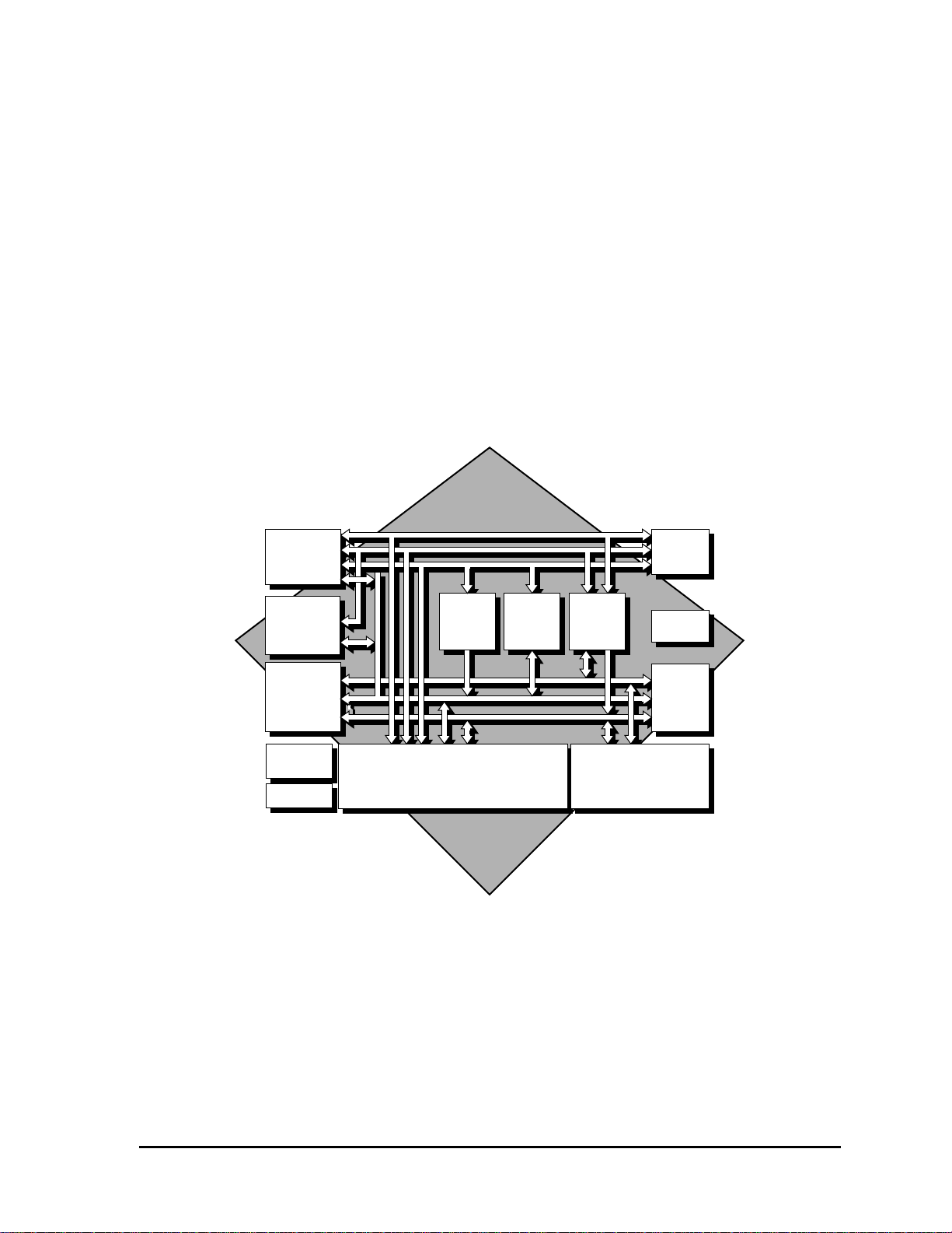
The DSP56012 is a member of the 24-bit DSP56000 family. The DSP is composed of
the 24-bit DSP56000 core, memory, and a set of peripheral modules, as shown in
Figure 1-1. The 24-bit DSP56000 core is composed of a Data Arithmetic Logic Unit
(ALU), an Address Generation Unit (AGU), a Program Controller, an On-Chip
Emulation (OnCE) port, and a PLL designed to allow the DSP to run at full speed
while using a low-speed clock. The DSP56000-family architecture, upon which the
DSP56012 is built, was designed to maximize throughput in data-intensive digital
signal processing applications. The result is a dual-natured, expandable architecture
with sophisticated on-chip peripherals and versatile GPIO.
1-8 DSP56012 User’s Manual MOTOROLA
Page 29
Overview
DSP56012 Architectural Overview
Parallel
Host
Interface
(HI)
24-Bit
DSP56000
Core
Internal
OnCETM Port
Clock
PLL
Gen.
EXTAL
15
Data
Bus
Switch
General
Purpose
I/O
(GPIO)
Controller
43
8
Interface
Program
Interrupt
IRQA
9
Serial
Audio
(SAI)
Address
Generation
Program Control Unit
4
, IRQB, NMI, RESET
Serial
Host
Interface
(SHI)
Unit
Program
Decode
Controller
5 2
Digital
Audio
Transmitter
(DAX)
GDB
PDB
XDB
YDB
Generator
Program
Address
PAB
XAB
YAB
Program
Memory
24 × 24 + 56 → 56-Bit MAC
Two 56-Bit Accumulators
X Data
Memory
Data ALU
16-Bit Bus
24-Bit Bus
Y Data
Memory
Expansion
Area
Figure 1-1 DSP56012 Block Diagram
The DSP56000 core is dual-natured in that there are two independent data memory
spaces, two address arithmetic units, and a Data ALU that has two accumulators and
two shifter/limiters. The duality of the architecture makes it easier to write software
for DSP applications. For example, data is naturally partitioned into coefficient and
data spaces for filtering and transformations, and into real and imaginary spaces for
performing complex arithmetic.
Note: Although the DSP56000 core has built-in support for external memory
expansion, the DSP56012 does not implement this function. For DSP56012
applications, external memory expansion is a function of the host processor.
The DSP56000 architecture is especially suited for audio applications since its
arithmetic operations are executed on 24-bit or 48-bit data words. This is a significant
advantage for audio over 16-bit and 32-bit architectures—16-bit DSP architectures
have insufficient precision for CD-quality sound, and while 32-bit DSP architectures
possess the necessary precision, with extra silicon and cost overhead they are not
suitable for high-volume, cost-driven audio applications
MOTOROLA DSP56012 User’s Manual 1-9
Page 30

Overview
DSP56012 Architectural Overview
1.3.1 Peripheral Modules
The following peripheral modules are included on the DSP56012:
• Parallel Host Interface—The Host Interface (HI) provides a byte-wide parallel
interface for parallel data transfer between the DSP56012 and a host processor
or another parallel peripheral device. The HI will operate with 8-, 16-, and
24-bit words
• Serial Host Interface (SHI)—The Serial Host Interface provides a fast, yet
simple serial interface to connect the DSP56012 to a host processor or to
another serial peripheral device. Two serial protocols are available: the
Motorola Serial Peripheral Interface (SPI) bus and the Philips Inter
Integrated-circuit Control (I
24-bit words and the receiver contains an optimal 10-word First-In, First-Out
(FIFO) register to reduce the receive interrupt rate.
• Serial Audio Interface (SAI)—The SAI provides a synchronous serial
interface that allows the DSP56012 to communicate using a wide range of
standard serial data formats used by audio manufacturers at bit rates up to
one third the DSP core clock rate (e.g., 27 MHz for an 81 MHz clock). There
are three synchronized data transmission lines and two synchronized data
reception lines, all of which are double-buffered.
2
C) bus. The SHI will operate with 8-, 16-, and
• General Purpose Input/Output (GPIO)—The GPIO has eight dedicated
signal lines that can be independently programmed to be inputs, standard
TTL outputs, open collector outputs, or disconnected.
• Digital Audio Transmitter (DAX)—The DAX is a serial audio interface
module that outputs digital audio data in AES/EBU, CP-340, and IEC958
formats.
1.3.2 DSP Core Processor
The 24-bit DSP56000 core is composed of a Data ALU, an AGU, a program controller,
and the buses that connect them together. The OnCE port and a PLL are integral
parts of this processor. Figure 1-1 on page 1-9 illustrates the DSP block diagram,
showing the components of the core processor, as well as the peripherals specific to
the DSP56012. The following paragraphs present a brief overview of the DSP56000
core processor. For more thorough detail, refer to the
DSP56000 Family Manual
.
1-10 DSP56012 User’s Manual MOTOROLA
Page 31

Overview
DSP56012 Architectural Overview
1.3.2.1 Data Arithmetic and Logic Unit (Data ALU)
The Data Arithmetic and Logic Unit (Data ALU) has been designed to be fast and
provide the capability to process signals having a wide dynamic range. Special
circuitry has been provided to facilitate the processing of data overflows and
round-off errors. The Data ALU performs all of the arithmetic and logical
operations on data operands. The Data ALU consists of four 24-bit input registers,
two 48-bit accumulator registers (also usable as four 24-bit accumulators), two 8-bit
accumulator extension registers, an accumulator shifter, two data shifter/limiters,
and a parallel single-cycle non-pipelined Multiplier-Accumulator (MAC). Data
ALU operations use fractional two’s-complement arithmetic. Data ALU registers
may be read or written over the X Data Bus (XDB) and Y Data Bus (YDB) as 24- or
48-bit operands. The 24-bit data words provide 144 dB of dynamic range. This is
sufficient for most real-world applications, including high-quality audio
applications, since the majority of Analog-to-Digital (A/D) and Digital-to-Analog
(D/A) converters are 16 bits or less, and certainly not greater than 24 bits. The 56-bit
accumulation internal to the Data ALU provides 336 dB of internal dynamic range,
assuring no loss of precision due to intermediate processing.
Two data shifter/limiters provide special post-processing on data reads (from the
Data ALU accumulator registers and directed to the XDB or YDB). The data shifters
are capable of shifting data one bit to the left or to the right, as well as passing the
data unshifted. Each data shifter has a 24-bit output with overflow indication. The
data shifters are controlled by scaling-mode bits. These shifters permit no-overhead
dynamic scaling of fixed point data by simply programming the scaling mode bits.
This permits block floating-point algorithms to be implemented efficiently. For
example, Fast Fourier Transform (FFT) routines can use this feature to selectively
scale each butterfly pass. Saturation arithmetic is accommodated to minimize errors
due to overflow. Overflow occurs when a source operand requires more bits for
accurate representation than there are available in the destination. To minimize the
error due to overflow, “limiting” causes the maximum (or minimum, if negative)
value to be written to the destination with an error flag.
1.3.2.2 Address Generation Unit (AGU)
The Address Generation Unit (AGU) performs all address storage and effective
address calculations necessary to access data operands in memory. It implements
three types of arithmetic to update addresses—linear, modulo, and reverse carry.
This unit operates in parallel with other chip resources to minimize address
generation overhead. The AGU contains eight address registers R[7:0] (i.e., Rn), eight
offset registers N[7:0] (i.e., Nn), and eight modifier registers M[7:0] (i.e., Mn). The Rn
are 16-bit registers that may contain an address or data. Each Rn register may
provide addresses to the X memory Address Bus (XAB), Y memory Address Bus
(YAB), and the Program Address Bus (PAB). The Nn and Mn registers are 16-bit
registers that are normally used to update the Rn registers, but may be used for data.
MOTOROLA DSP56012 User’s Manual 1-11
Page 32

Overview
DSP56012 Architectural Overview
AGU registers may be read from or written to via the Global Data Bus as 16-bit
operands. The AGU has two modulo arithmetic units that can generate two
independent 16-bit addresses every instruction cycle for any two of the XAB, YAB, or
PAB.
1.3.2.3 Program Control Unit
The program control unit performs instruction prefetch, instruction decoding,
hardware DO loop control, and exception processing. It contains six directly
addressable registers—the Program Counter (PC), Loop Address (LA), Loop Counter
(LC), Status Register (SR), Operating Mode Register (OMR), and Stack Pointer (SP).
The program control unit also contains a 15 level by 32-bit system stack memory. The
16-bit PC can address 65,536 (64 K) locations in program memory space.
1.3.2.4 Data Buses
Data movement on the chip occurs over four bidirectional 24-bit buses—the X Data
Bus (XDB), the Y Data Bus (YDB), the Program Data Bus (PDB), and the Global Data
Bus (GDB). Certain instructions concatenate XDB and YDB to form a 48-bit data bus.
Data transfers between the Data ALU and the two data memories, X and Y, occur
over the XDB and YDB, respectively. These transfers can occur simultaneously on the
DSP, maximizing data throughput. All other data transfers, such as I/O transfers to
internal peripherals, occur over the GDB. Instruction word pre-fetches take place
over the PDB in parallel with data transfers. Transfers between buses are
accomplished through the internal bus switch.
1.3.2.5 Address Buses
Addresses are specified for internal X data memory and Y data memory using two
unidirectional 16-bit buses—the X Address Bus (XAB) and the Y Address Bus (YAB).
program memory addresses are specified using the 16-bit Program Address Bus
(PAB).
1.3.2.6 Phase Lock Loop (PLL)
The Phase Lock Loop (PLL) reduces the need for multiple oscillators in a system
design, thus reducing the overall system cost. An additional benefit of the PLL is that
it permits the use of a low-frequency external clock with no sacrifice of processing
speed. The PLL converts the low-frequency external clock to the high speed internal
clock needed to run the DSP at maximum speed. This diminishes the electromagnetic
interference generated by high frequency clocking. The PLL performs frequency
multiplication to allow the processor to use almost any available external system
clock for full-speed operation. It also improves the synchronous timing of the
processor’s external memory port, significantly reducing the timing skew between
EXTAL and the internal chip phases when the Multiplication Factor (MF) ≤ 4. The
PLL is unique in that it provides a low power divider on its output, which can reduce
or restore the chip operating frequency without losing the PLL lock.
1-12 DSP56012 User’s Manual MOTOROLA
Page 33

Overview
DSP56012 Architectural Overview
1.3.2.7 On-Chip Emulation (OnCE) Port
The On-Chip Emulation (OnCE) port provides a sophisticated debugging tool that
allows simple, inexpensive, and speed-independent access to the processor’s internal
registers and peripherals. The OnCE port tells the application programmer the exact
status of most of the on-chip registers, memory locations, and buses, as well as
storing the addresses of the last five instructions that were executed.
1.3.3 Memories
The three independent memory spaces of the DSP56012—X data, Y data, and
program—and their configurations are discussed briefly here. See Section 3
Memory, Operating Modes, and Interrupts
for more detail.
1.3.3.1 Program Memory
The on-chip program memory is 24-bits wide. Addresses are received from the
Program Control Logic (usually the Program Counter) over the Program Address
Bus (PAB). Program memory may be written using MOVEM instructions. The
interrupt vectors are located in the bottom 128 locations of program memory.
Table 1-3 lists the interrupt vector addresses and indicates the Interrupt Priority
Level (IPL) of each interrupt source. Program RAM has many advantages. It
provides a means to develop code efficiently. Programs can be changed dynamically,
allowing efficient overlaying of DSP software algorithms. In this way the on-chip
Program RAM operates as a fixed cache, thereby minimizing accesses to slower
external memory.
,
The Bootstrap mode, described in Appendix A, provides a convenient, low-cost
method to load the DSP56012 Program RAM through the HI or the SHI (using either
2
SPI or I
C formats) after a power-on reset.
Table 1-3 Interrupt Starting Addresses and Sources
Interrupt
Starting Address
P:$0000 3 Hardware RESET
P:$0002 3 Stack Error
P:$0004 3 Trace
P:$0006 3 SWI
P:$0008 0–2 IRQA
P:$000A 0–2 IRQB
P:$000C Reserved
IPL Interrupt Source
MOTOROLA DSP56012 User’s Manual 1-13
Page 34

Overview
DSP56012 Architectural Overview
Table 1-3 Interrupt Starting Addresses and Sources (Continued)
Interrupt
Starting Address
P:$000E Reserved
P:$0010 0–2 SAI Left Channel Transmitter if TXIL = 0
P:$0012 0–2 SAI Right Channel Transmitter if TXIL = 0
P:$0014 0–2 SAI Transmitter Exception if TXIL = 0
P:$0016 0–2 SAI Left Channel Receiver if RXIL = 0
P:$0018 0–2 SAI Right Channel Receiver if RXIL = 0
P:$001A 0–2 SAI Receiver Exception if RXIL = 0
P:$001C Reserved
P:$001E 3 NMI
P:$0020 0–2 SHI Transmit Data
P:$0022 0–2 SHI Transmit Underrun Error
P:$0024 0–2 SHI Receive FIFO Not Empty
P:$0026 Reserved
P:$0028 0–2 SHI Receive FIFO Full
P:$002A 0–2 SHI Receive Overrun Error
P:$002C 0–2 SHI Bus Error
IPL Interrupt Source
P:$002E Reserved
P:$0030 0–2 Host Receive Data
P:$0032 0–2 Host Transmit Data
P:$0034 0–2 Host Command (default)
P:$0036 Reserved; available for Host Command, see p. B-5–B-6.
::
P:$003C Reserved; available for Host Command, see p. B-5–B-6.
P:$003E 3 Illegal Instruction
P: $0040 0–2 SAI Left Channel Transmitter if TXIL = 1
P: $0042 0–2 SAI Right Channel Transmitter if TXIL = 1
P: $0044 0–2 SAI Transmitter Exception if TXIL = 1
P: $0046 0–2 SAI Left Channel Receiver if RXIL = 1
P: $0048 0–2 SAI Right Channel Receiver if RXIL = 1
P: $004A 0–2 SAI Receiver Exception if RXIL = 1
P: $004C Reserved; available for Host Command, see p. B-5–B-6.
P: $004E Reserved; available for Host Command, see p. B-5–B-6.
1-14 DSP56012 User’s Manual MOTOROLA
Page 35

DSP56012 Architectural Overview
Table 1-3 Interrupt Starting Addresses and Sources (Continued)
Overview
Interrupt
Starting Address
P: $0050 0–2 DAX Transmit Underrun Error
P: $0052 0–2 DAX Block Transferred
P: $0054 Reserved; available for Host Command, see p. B-5–B-6.
P: $0056 0–2 DAX Transmit Register Empty
P: $0058 Reserved; available for Host Command, see p. B-5–B-6.
: Reserved; available for Host Command, see p. B-5–B-6.
P: $007E Reserved; available for Host Command, see p. B-5–B-6.
IPL Interrupt Source
1.3.3.2 X Data Memory
The on-chip X data memory shown in Table 1-4 is 24 bits wide. Addresses are
received from the XAB, and data transfers to the Data ALU occur on the XDB.
1.3.3.3 Y Data Memory
The on-chip Y data memory shown in Table 1-4 is 24 bits wide. Addresses are
received from the YAB, and data transfers to the Data ALU occur on the YDB.
1.3.3.4 On-Chip Memory Configuration Bits
Through the use of bits PEA and PEB in the OMR, four different memory
configurations are possible. These configurations provide appropriate memory sizes
for a variety of applications (see Table 1-4). Section 3 provides detailed information
about memory configuration.
Table 1-4 Internal Memory Configurations
No Switch
(PEA = 0
PEB = 0)
Program RAM 0.25 K 1.0 K 1.75 K 2.5 K
X RAM 4.0 K 3.25 K 3.25 K 2.5 K
Y RAM 4.25 K 4.25 K 3.5 K 3.5 K
Program ROM 15 K 15 K 15 K 15 K
X ROM 3.5 K 3.5 K 3.5 K 3.5 K
Y ROM 2.0 K 2.0 K 2.0 K 2.0 K
Switch A
(PEA = 1
PEB = 0)
Switch B
(PEA = 0
PEB = 1)
Switch A+B
(PEA = 1
PEB = 1)
MOTOROLA DSP56012 User’s Manual 1-15
Page 36

Overview
DSP56012 Architectural Overview
1.3.3.5 Memory Configuration Bits
Through the use of bits PEA and PEB in the Operating Mode Register (OMR), four
different memory configurations are possible, to provide appropriate memory sizes
for a variety of applications (see Table 1-4).
1.3.3.6 External Memory
The DSP56012 does not extend internal memory off chip.
1.3.3.7 Bootstrap ROM
The bootstrap ROM occupies locations 0–31 ($0–$1F) in the memory map on the
DSP56012. The bootstrap ROM is factory- programmed to perform the bootstrap
operation following hardware reset. It downloads a 256-word user program from
2
either the HI port or the SHI port (in SPI or I
C format). The bootstrap ROM activity
is controlled by the bits MC, MB, and MA, which are located in the OMR. When in
the Bootstrap mode, the first 256 words of program RAM are read-disabled but
write-accessible. The contents of the bootstrap ROM are listed in Appendix A.
1.3.3.8 Reserved Memory Spaces
The memory spaces marked as reserved should not be accessed by the user. They are
reserved for the expansion of future versions or variants of this DSP. Write
operations to the reserved range are ignored. Read operations from addresses in the
reserved range (with values greater than or equal to $2E00 in X memory space and
$2800 in Y memory space, and values from the reserved area of program memory
space), return the value $000005, which is the opcode for the ILLEGAL instruction,
and causes an illegal instruction interrupt service. If a read access is performed from
the reserved area below address $2000 in X or Y data memory, the resulting data will
be undetermined. If an instruction fetch is attempted from addresses in the reserved
area, the value returned is $000005 (ILLEGAL opcode).
1.3.4 Input/Output
A variety of system configurations are facilitated by the DSP56012 Input/Output
(I/O) structure. Each I/O interface has its own control, status, and double-buffered
data registers that are memory-mapped in the X-data memory space (see Table 1-5).
The HI, SHI, SAI , and DAX also have several dedicated interrupt vector addresses
and control bits to enable and disable interrupts (see Table 1-3 on page 1-13). These
interrupt vectors minimize the overhead associated with servicing an interrupt by
immediately executing the appropriate service routine. Each interrupt can be
configured to one of three maskable priority levels.
1-16 DSP56012 User’s Manual MOTOROLA
Page 37

Table 1-5 On-chip Peripheral Memory Map
Address Register
X:$FFFF Interrupt Priority Register (IPR)
X:$FFFE Reserved
X:$FFFD PLL Control Register (PCTL)
X:$FFFC Reserved
X:$FFFB Reserved
X:$FFFA Reserved
X:$FFF9 Reserved
X:$FFF8 Reserved
X:$FFF7 GPIO Control/Data Register (GPIOR)
X:$FFF6 Reserved
X:$FFF5 Reserved
X:$FFF4 Reserved
Overview
DSP56012 Architectural Overview
X:$FFF3 SHI Receive FIFO/Transmit Register (HRX/HTX)
X:$FFF2
X:$FFF1 SHI Host Control/Status Register (HCSR)
X:$FFF0 SHI Host Clock Control Register (HCKR)
X:$FFEF Reserved
X:$FFEE Port B Data Register (PBD)
X:$FFED Port B Data Direction Register (PBDDR)
X:$FFEC Port B Control Register (PBC)
X:$FFEB Host Receive/Transmit Register (HORX/HOTX)
X:$FFEA Reserved
X:$FFE9 Host Status Register (HSR)
X:$FFE8 Host Control Register (HCR)
X:$FFE7 SAI TX2 Data RegisteR (TX2)
X:$FFE6 SAI TX1 Data Register (TX1)
X:$FFE5 SAI TX0 Data Register (TX0)
X:$FFE4 SAI TX Control/Status Register (TCS)
X:$FFE3 SAI RX1 Data Register (RX1)
2
C Slave Address Register (HSAR)
SHI I
X:$FFE2 SAI RX0 Data Register (RX0)
X:$FFE1 SAI RX Control/Status Register (RCS)
X:$FFE0 SAI Baud Rate Control Register (BRC)
X:$FFDF DAX Status Register (XSTR)
MOTOROLA DSP56012 User’s Manual 1-17
Page 38

Overview
DSP56012 Architectural Overview
Table 1-5 On-chip Peripheral Memory Map (Continued)
Address Register
X:$FFDE DAX Control Register (XCTR)
X:$FFDD Reserved
X:$FFDC DAX Transmit Data Registers (XADRA/XADRB)
X:$FFDB Reserved
::
X:$FFC0 Reserved
1.3.4.1 Parallel Host Interface (HI)
The parallel Host Interface (HI) is a byte-wide, full-duplex, double-buffered, parallel
port that can be connected directly to the data bus of a host processor. The host
processor can be any of a number of industry-standard microcomputers or
microprocessors, another DSP, or DMA hardware, because this interface looks like
static memory to the host processor. The HI is asynchronous and consists of two sets
of registers—one set accessible only to the host processor and a second set accessible
only to the DSP CPU (see Section 4, Parallel Host Interface).
1.3.4.2 Serial Host Interface (SHI)
The Serial Host Interface (SHI) provides a serial path for communication and
program/coefficient data transfers between the DSP and an external host processor
or other serial peripheral devices. This interface can connect directly to one of two
well-known and widely-used synchronous serial buses: the Serial Peripheral
2
Interface (SPI) bus defined by Motorola and the Inter Integrated-circuit Control (I
2
bus defined by Philips. The SHI handles both SPI and I
C bus protocols as required
C)
from a slave or a single-master device. In order to minimize DSP overhead, the SHI
supports single-, double-, and triple-byte data transfers. An optimal ten-word receive
FIFO register reduces the DSP overhead for data reception (see Section 5, Serial
Host Interface).
1-18 DSP56012 User’s Manual MOTOROLA
Page 39

Overview
DSP56012 Architectural Overview
1.3.4.3 Serial Audio Interface (SAI)
The DSP can communicate with other devices through its serial audio interfaces. The
Serial Audio Interface (SAI) provides a synchronous full-duplex serial port for serial
connection with a variety of audio devices such as Analog-to-Digital (A/D)
converters, Digital-to-Analog (D/A) converters, Compact Disc (CD) devices, etc. The
SAI implements a wide range of serial data formats in use by audio manufacturers.
Examples are:
2
S format (Philips)
•I
• CDP format (Sony)
• MEC format (Matsushita)
• Most industry-standard serial A/D and D/A formats
The SAI consists of independent transmit and receive sections and a common baud
rate generator. The transmitter consists of three transmitters controlled by one
transmitter controller. This enables simultaneous data transmission to as many as
three stereo audio devices, or transmission of three separate stereo pairs of audio
channels. The receiver consists of two receivers and a single receive controller. This
enables simultaneous data reception from up to two stereo audio devices. The
transmit and receive sections are fully asynchronous and may transmit and receive at
different rates (see Section 6, Serial Audio Interface).
1.3.4.4 General Purpose I/O
The General Purpose Input/Output (GPIO) pins are used for control and handshake
functions between the DSP and external circuitry. The GPIO port has eight dedicated
pins (GPIO0–GPIO7) that are controlled through a memory-mapped register.
Associated with each GPIO pin is a data bit, a control bit, and a data direction bit that
configures the pin as an input or an output, open-collector or normal (see Section 7,
GPIO).
1.3.4.5 Digital Audio Transmitter (DAX)
The Digital Audio Transmitter (DAX) is a serial audio interface module that outputs
digital audio data in the AES/EBU, CP-340, and IEC958 formats. The DAX transmits
one frame (consisting of two sub-frames) of audio and non-audio data at a time.
However, the DAX data path is double buffered so the next frame data can be stored
in the DAX without affecting the frame currently being transmitted (see Section 8,
Digital Audio Transmitter).
MOTOROLA DSP56012 User’s Manual 1-19
Page 40

Overview
DSP56012 Architectural Overview
1-20 DSP56012 User’s Manual MOTOROLA
Page 41

SECTION 2
SIGNAL DESCRIPTIONS
MOTOROLA DSP56012 User’s Manual 2-1
Page 42

Signal Descriptions
2.1 SIGNAL GROUPINGS. . . . . . . . . . . . . . . . . . . . . . . . . . . . . . 2-3
2.2 POWER. . . . . . . . . . . . . . . . . . . . . . . . . . . . . . . . . . . . . . . . . 2-5
2.3 GROUND. . . . . . . . . . . . . . . . . . . . . . . . . . . . . . . . . . . . . . . . 2-6
2.4 PHASE LOCK LOOP (PLL). . . . . . . . . . . . . . . . . . . . . . . . . . 2-7
2.5 INTERRUPT AND MODE CONTROL. . . . . . . . . . . . . . . . . . 2-8
2.6 HOST INTERFACE (HI) . . . . . . . . . . . . . . . . . . . . . . . . . . . 2-10
2.7 SERIAL HOST INTERFACE (SHI) . . . . . . . . . . . . . . . . . . . 2-13
2.8 SERIAL AUDIO INTERFACE (SAI). . . . . . . . . . . . . . . . . . . 2-16
2.9 GENERAL PURPOSE INPUT/OUTPUT (GPIO). . . . . . . . . 2-18
2.10 DIGITAL AUDIO INTERFACE (DAX) . . . . . . . . . . . . . . . . . 2-18
2.11 OnCE PORT . . . . . . . . . . . . . . . . . . . . . . . . . . . . . . . . . . . . 2-19
2-2 DSP56012 User’s Manual MOTOROLA
Page 43

Signal Descriptions
Signal Groupings
2.1 SIGNAL GROUPINGS
The DSP56012 input and output signals are organized into the ten functional groups
shown in Table 2-1. The individual signals are shown in Figure 2-1 on page 2-4.
Table 2-1 DSP56012 Functional Signal Groupings
Functional Group
Power (VCC) 13 Table 2-2
Ground (GND) 17 Table 2-3
PLL 4 Table 2-4
Interrupt and Mode Control 4 Table 2-5
Host Interface (HI) Port B 15 Table 2-6
Serial Host Interface (SHI) 5 Table 2-7
Serial Audio Interface (SAI) 9 Table 2-8
General Purpose Input/Output (GPIO) 8 Table 2-10
Digital Audio Transmitter (DAX) 2 Table 2-11
OnCE Port 4 Table 2-12
Number of
Signals
Detailed
Description
Table 2-9
MOTOROLA DSP56012 User’s Manual 2-3
Page 44

Signal Descriptions
Signal Groupings
V
V
V
V
V
V
CCP
CCQ
CCA
CCD
CCH
CCS
4
2
1
3
2
Power Inputs:
PLL
Internal Logic
A
D
HI
SHI
DSP56012
Host
Interface
(HI) Port
8
H0–H7
HOA0
HOA1
HOA2
HR/W
HEN
HOREQ
HACK
Port B GPIO
PB0–PB7
PB8
PB9
PB10
PB11
PB12
PB13
PB14
GND
GND
GND
GND
GND
GND
PLOCK
PCAP
PINIT
EXTAL
MODA/IRQA
MODB/IRQB
MODC/NMI
RESET
Grounds:
4
3
2
4
3
PLL
Internal Logic
A
D
HI
SHI
PLL
Interrupt
/Mode
Control
Serial Host
Interface (SHI)
Serial Audio
Interface (SAI)
Rec0
Rec1
Tran0
Tran1
Tran2
General Purpose
Input/Output (GPIO)
Digital Audio
Transmitter (DAX)
8
MOSI/HA0
/HA2
SS
MISO/SDA
SCK/SCL
HREQ
WSR
SCKR
SDI0
SDI1
WST
SCKT
SDO0
SDO1
SDO2
GPIO0–GPIO7
ADO
ACI
P
Q
A
D
H
S
OnCE™
Port
DSCK/OS1
DSI/OS0
DSO
DR
Figure 2-1 DSP56012 Signals
2-4 DSP56012 User’s Manual MOTOROLA
Page 45

2.2 POWER
Table 2-2 Power Inputs
Power Name Description
Signal Descriptions
Power
V
V
V
V
V
V
CCP
CCQ
CCA
CCD
CCH
CCS
PLL Power—V
is VCC dedicated for Phase Lock Loop (PLL) use. The voltage
CCP
should be well-regulated and the input should be provided with an extremely
low impedance path to the VCC power rail. V
should be bypassed to GNDP
CCP
by a 0.1 µF capacitor located as close as possible to the chip package.
Quiet Power—V
is an isolated power for the internal processing logic. This
CCQ
input must be tied externally to all other chip power inputs. The user must
provide adequate external decoupling capacitors.
A Power—V
is an isolated power for sections of the internal chip logic. This
CCA
input must be tied externally to all other chip power inputs. The user must
provide adequate external decoupling capacitors.
D Power—V
is an isolated power for sections of the internal chip logic. This
CCD
input must be tied externally to all other chip power inputs. The user must
provide adequate external decoupling capacitors.
Host Power—V
is an isolated power for the HI I/O drivers. This input must
CCH
be tied externally to all other chip power inputs. The user must provide adequate
external decoupling capacitors.
Serial Host Power—V
is an isolated power for the SHI I/O drivers. This
CCS
input must be tied externally to all other chip power inputs. The user must
provide adequate external decoupling capacitors.
MOTOROLA DSP56012 User’s Manual 2-5
Page 46

Signal Descriptions
Ground
2.3 GROUND
Table 2-3 Grounds
Ground Name Description
GND
P
GNDQ Internal Logic Ground—GNDQ is an isolated ground for the internal processing
GNDA A Ground—GNDA is an isolated ground for sections of the internal logic. This
GNDD D Ground—GNDD is an isolated ground for sections of the internal logic. This
GND
H
GND
S
PLL Ground—GNDP is ground dedicated for PLL use. The connection should be
provided with an extremely low-impedance path to ground. V
bypassed to GNDP by a 0.1 µF capacitor located as close as possible to the chip
package.
logic. This connection must be tied externally to all other chip ground
connections. The user must provide adequate external decoupling capacitors.
connection must be tied externally to all other chip ground connections. The user
must provide adequate external decoupling capacitors.
connection must be tied externally to all other chip ground connections. The user
must provide adequate external decoupling capacitors.
Host Ground—GNDH is an isolated ground for the HI I/O drivers. This
connection must be tied externally to all other chip ground connections. The user
must provide adequate external decoupling capacitors.
Serial Host Ground—GNDS is an isolated ground for the SHI I/O drivers. This
connection must be tied externally to all other chip ground connections. The user
must provide adequate external decoupling capacitors.
should be
CCP
2-6 DSP56012 User’s Manual MOTOROLA
Page 47

2.4 PHASE LOCK LOOP (PLL)
Table 2-4 Phase Lock Loop Signals
Signal Descriptions
Phase Lock Loop (PLL)
Signal Name Type
PLOCK Output Indeterminate Phase Locked—PLOCK is an output signal that, when
PCAP Input Input PLL Capacitor—PCAP is an input connecting an off-chip
PINIT Input Input PLL Initial—During assertion of RESET, the value of
EXTAL Input Input External Clock/Crystal Input—EXTAL interfaces the
State During
Reset
Signal Description
driven high, indicates that the PLL has achieved phase
lock. After Reset, PLOCK is driven low until lock is
achieved.
Note: PLOCK is a reliable indicator of the PLL lock
state only after the chip has exited the Reset
state. During hardware reset, the PLOCK state is
determined by PINIT and the current PLL lock
condition.
capacitor to the PLL filter. Connect one capacitor
terminal to PCAP and the other terminal to V
If the PLL is not used, PCAP may be tied to VCC, GND,
or left floating.
PINIT is written into the PLL Enable (PEN) bit of the PLL
Control Register, determining whether the PLL is
enabled or disabled.
internal crystal oscillator input to an external crystal or
an external clock.
CCP
.
MOTOROLA DSP56012 User’s Manual 2-7
Page 48

Signal Descriptions
Interrupt and Mode Control
2.5 INTERRUPT AND MODE CONTROL
Table 2-5 Interrupt and Mode Control
Signal Name Type
MODA/IRQA Input Input Mode Select A/External Interrupt Request A—This
MODB/IRQB Input Input Mode Select B/External Interrupt Request B—This input
State During
Reset
Signal Description
input has two functions:
1. to select the initial chip operating mode, and
2. after synchronization, to allow an external device
to request a DSP interrupt.
MODA is read and internally latched in the DSP when the
processor exits the Reset state. MODA, MODB, and
MODC select the initial chip operating mode. Several
clock cycles (depending on PLL stabilization time) after
leaving the Reset state, the MODA signal changes to
external interrupt request IRQA. The chip operating
mode can be changed by software after reset. The IRQA
input is a synchronized external interrupt request that
indicates that an external device is requesting service. It
may be programmed to be level-sensitive or
negative-edge-sensitive. If the processor is in the Stop
state and IRQA is asserted, the processor will exit the Stop
state.
has two functions:
1. to select the initial chip operating mode, and
2. after internal synchronization, to allow an
external device to request a DSP interrupt.
MODB is read and internally latched in the DSP when the
processor exits the Reset state. MODA, MODB, and
MODC select the initial chip operating mode. Several
clock cycles (depending on PLL stabilization time) after
leaving the Reset state, the MODB signal changes to
external interrupt request IRQB. After reset, the chip
operating mode can be changed by software. The IRQB
input is an external interrupt request that indicates that
an external device is requesting service. It may be
programmed to be level-sensitive or
negative-edge-triggered.
2-8 DSP56012 User’s Manual MOTOROLA
Page 49

Interrupt and Mode Control
Table 2-5 Interrupt and Mode Control (Continued)
Signal Descriptions
Signal Name Type
MODC/NMI Input Input Mode Select C/Non-maskable Interrupt Request— This
RESET Input Input Reset—This input is a direct hardware reset on the
State During
Reset
Signal Description
input has two functions:
1. to select the initial chip operating mode, and
2. after internal synchronization, to allow an
external device to request a non-maskable DSP
interrupt.
MODC is read and internally latched in the DSP when the
processor exits the Reset state. MODA, MODB, and
MODC select the initial chip operating mode. Several
clock cycles (depending on PLL stabilization time) after
leaving the Reset state, the MODC signal changes to the
nonmaskable external interrupt request NMI
the chip operating mode can be changed by software. The
NMI input is an external interrupt request that indicates
that an external device is requesting service. It may be
programmed to be level-sensitive or
negative-edge-sensitive.
processor. When RESET is asserted low, the DSP is
initialized and placed in the Reset state. A Schmitt trigger
input is used for noise immunity. When the RESET signal
is deasserted, the initial chip operating mode is latched
from the MODA, MODB, and MODC signals. The
internal reset signal is deasserted synchronous with the
internal clocks. In addition, the PINIT pin is sampled and
written into the PEN bit of the PLL Control Register.
. After reset,
MOTOROLA DSP56012 User’s Manual 2-9
Page 50

Signal Descriptions
Host Interface (HI)
2.6 HOST INTERFACE (HI)
The HI provides a fast parallel data to 8-bit port, which may be connected directly
to the host bus. The HI supports a variety of standard buses, and can be directly
connected to a number of industry standard microcomputers, microprocessors,
DSPs, and DMA hardware.
Table 2-6 Host Interface
Signal Name Type
H0–H7
PB0–PB7
HOA0–HOA2
PB8–PB10
Input/
Output
Input
Input/
Output
State During
Reset
Input Host Data Bus (H0–H7)—This data bus transfers data
between the host processor and the DSP56012.
When configured as a Host Interface port, the
H0–H7signals are tri-stated as long as HEN is
deasserted. The signals are inputs unless HR/W is high
and HEN is asserted, in which case H0–H7 become
outputs, allowing the host processor to read the
DSP56012 data. H0–H7 become outputs when HACK is
asserted during HOREQ assertion.
Port B GPIO 0–7 (PB0–PB7)—These signals are General
Purpose I/O signals (PB0–PB7) when the Host Interface is
not selected.
After reset, the default state for these signals is GPIO
input.
Input Host Address 0 – Host Address 2
(HOA0–HOA2)—These inputs provide the address
selection for each Host Interface register.
Port B GPIO 8–10 (PB8–PB10)—These signals are
General Purpose I/O signals (PB8–PB10) when the Host
Interface is not selected.
Signal Description
After reset, the default state for these signals is GPIO
input.
2-10 DSP56012 User’s Manual MOTOROLA
Page 51

Table 2-6 Host Interface (Continued)
Signal Descriptions
Host Interface (HI)
Signal Name Type
HR/W
PB11
HEN
Input
Input/
Output
Input
State During
Reset
Input Host Read/Write—This input selects the direction of
data transfer for each host processor access. If HR/W is
high and HEN is asserted, H0–H7 are outputs and DSP
data is transferred to the host processor. If HR/W is low
and HEN is asserted, H0–H7 are inputs and host data is
transferred to the DSP. HR/W must be stable when
HEN is asserted.
Port B GPIO 11 (PB11)—This signal is a General
Purpose I/O signal (PB11) when the Host Interface is
not being used.
After reset, the default state for this signal is GPIO
input.
Input Host Enable—This input enables a data transfer on the
host data bus. When HEN is asserted and HR/W is
high, H0–H7 become outputs and the host processor
may read DSP56011 data. When HEN is asserted and
HR/W is low, H0–H7 become inputs. Host data is
latched inside the DSP on the rising edge of HEN.
Normally, a chip select signal derived from host address
decoding and an enable strobe are used to generate
HEN.
Signal Description
PB12
HOREQ
PB13
Input/
Output
Open-
drain
Output
Input/
Output
Port B GPIO 12 (PB12)—This signal is a General
Purpose I/O signal (PB12) when the Host Interface is
not being used.
After reset, the default state for this signal is GPIO
input.
Input Host Request— This signal is used by the Host Interface
to request service from the host processor, DMA
controller, or a simple external controller.
Note: HOREQ should always be pulled high when it
is not in use.
Port B GPIO 13 (PB13)—This signal is a General
Purpose (not open-drain) I/O signal (PB13) when the
Host Interface is not selected.
After reset, the default state for this signal is GPIO
input.
MOTOROLA DSP56012 User’s Manual 2-11
Page 52

Signal Descriptions
Host Interface (HI)
Table 2-6 Host Interface (Continued)
Signal Name Type
HACK
PB14
Input
Input/
Output
State During
Reset
Input Host Acknowledge— This input has two functions. It
provides a host acknowledge handshake signal for
DMA transfers and it receives a host interrupt
acknowledge compatible with MC68000 family
processors.
Note: HACK should always be pulled high when it is
not in use.
Port B GPIO 14 (PB14)—This signal is a General
Purpose I/O signal (PB14) when the Host Interface is
not selected.
After reset, the default state for this signal is GPIO
input.
Signal Description
2-12 DSP56012 User’s Manual MOTOROLA
Page 53

2.7 SERIAL HOST INTERFACE (SHI)
Signal Descriptions
Serial Host Interface (SHI)
Signal
Name
SCK/
SCL
The SHI has five I/O signals that can be configured to allow the SHI to operate in
either SPI or I
2
C mode.
Table 2-7 Serial Host Interface (SHI) Signals
Signal
Type
Input or
Output
State
during
Reset
Tri-stated SPI Serial Clock/I2C Serial Clock—The SCK signal is an
output when the SPI is configured as a master, and a
Schmitt-trigger input when the SPI is configured as a slave.
When the SPI is configured as a master, the SCK signal is
derived from the internal SHI clock generator. When the SPI
is configured as a slave, the SCK signal is an input, and the
clock signal from the external master synchronizes the data
transfer. The SCK signal is ignored by the SPI if it is defined
as a slave and the Slave Select (SS) signal is not asserted. In
both the master and slave SPI devices, data is shifted on one
edge of the SCK signal and is sampled on the opposite edge
where data is stable. Edge polarity is determined by the SPI
transfer protocol. SCL carries the clock for I2C bus
transactions in the I2C mode. SCL is a Schmitt-trigger input
when configured as a slave, and an open-drain output when
configured as a master. SCL should be connected to VCC
through a pull-up resistor.
Signal Description
The maximum allowed internally generated bit clock
frequency is f
mode where f
allowed externally generated bit clock frequency is f
the SPI mode and f
An external pull-up resistor is not required.
/4 for the SPI mode and f
osc
is the clock on EXTAL. The maximum
osc
/5 for the I2C mode
osc
/6 for the I2C
osc
osc
/3 for
MOTOROLA DSP56012 User’s Manual 2-13
Page 54

Signal Descriptions
Serial Host Interface (SHI)
Table 2-7 Serial Host Interface (SHI) Signals (Continued)
Signal
Name
MISO/
SDA
Signal
Type
Input or
Output
State
during
Reset
Tri-stated SPI Master-In-Slave-Out/I2C Data and
Acknowledge—When the SPI is configured as a master,
MISO is the master data input line. The MISO signal is used
in conjunction with the MOSI signal for transmitting and
receiving serial data. This signal is a Schmitt-trigger input
when configured for the SPI Master mode, an output when
configured for the SPI Slave mode, and tri-stated if
configured for the SPI Slave mode when SS
In I2C mode, SDA is a Schmitt-trigger input when receiving
and an open-drain output when transmitting. SDA should be
connected to VCC through a pull-up resistor. SDA carries the
data for I2C transactions. The data in SDA must be stable
during the high period of SCL. The data in SDA is only
allowed to change when SCL is low. When the bus is free,
SDA is high. The SDA line is only allowed to change during
the time SCL is high in the case of start and stop events. A
high to low transition of the SDA line while SCL is high is an
unique situation, which is defined as the start event. A low to
high transition of SDA while SCL is high is an unique
situation, which is defined as the stop event.
Signal Description
is deasserted.
MOSI/
HA0
Input or
Output
An external pull-up resistor is not required.
Tri-stated SPI Master-Out-Slave-In/I2C Slave Address 0—When the
SPI is configured as a master, MOSI is the master data output
line. The MOSI signal is used in conjunction with the MISO
signal for transmitting and receiving serial data. MOSI is the
slave data input line when the SPI is configured as a slave.
This signal is a Schmitt-trigger input when configured for the
SPI Slave mode.
This signal uses a Schmitt-trigger input when configured for
the I2C mode. When configured for I2C Slave mode, the HA0
signal is used to form the slave device address. HA0 is
ignored when it is configured for the I2C Master mode.
An external pull-up resistor is not required.
2-14 DSP56012 User’s Manual MOTOROLA
Page 55

Signal Descriptions
Serial Host Interface (SHI)
Table 2-7 Serial Host Interface (SHI) Signals (Continued)
Signal
Name
SS/HA2 Input Tri-stated SPI Slave Select/I2C Slave Address 2—This signal is an
HREQ Input or
Signal
Type
Output
State
during
Reset
active low Schmitt-trigger input when configured for the SPI
mode. When configured for the SPI Slave mode, this signal is
used to enable the SPI slave for transfer. When configured for
the SPI Master mode, this signal should be kept deasserted. If
it is asserted while configured as SPI master, a bus error
condition will be flagged.
This signal uses a Schmitt-trigger input when configured for
2
C mode. When configured for the I2C Slave mode, the
the I
HA2 signal is used to form the slave device address. HA2 is
ignored in the I2C Master mode. If SS is deasserted, the SHI
ignores SCK clocks and keeps the MISO output signal in the
high-impedance state.
This signal is tri-stated during hardware, software, or
personal reset (no need for external pull-up in this state).
Tri-stated Host Request—This signal is an active low Schmitt-trigger
input when configured for the Master mode, but an active
low output when configured for the Slave mode.
Signal Description
When configured for the Slave mode, HREQ is asserted to
indicate that the SHI is ready for the next data word transfer
and deasserted at the first clock pulse of the new data word
transfer. When configured for the Master mode, HREQ is an
input, and when asserted by the external slave device, it will
trigger the start of the data word transfer by the master. After
finishing the data word transfer, the master will await the
next assertion of HREQ to proceed to the next transfer.
This signal is tri-stated during hardware, software, personal
reset, or when the HREQ1–HREQ0 bits in the HCSR are
cleared (no need for external pull-up in this state).
MOTOROLA DSP56012 User’s Manual 2-15
Page 56

Signal Descriptions
Serial Audio Interface (SAI)
2.8 SERIAL AUDIO INTERFACE (SAI)
The SAI is composed of separate receiver and transmitter sections.
2.8.1 SAI Receive Section
The receive section of the SAI has four dedicated signals.
Table 2-8 Serial Audio Interface (SAI) Receive Signals
Signal
Name
SDI0 Input Tri-stated Serial Data Input 0—This is the receiver 0 serial data input.
SDI1 Input Tri-stated Serial Data Input 1—This is the receiver 1 serial data input.
SCKR Input or
WSR Input or
Signal
Type
Output
Output
State
during
Reset
This signal is high impedance during hardware or software
reset, while receiver 0 is disabled (R0EN = 0), or while the chip
is in the Stop state. No external pull-up resistor is required.
This signal is high impedance during hardware or software
reset, while receiver 1 is disabled (R1EN = 0), or while the chip
is in the Stop state. No external pull-up resistor is required.
Tri-stated Receive Serial Clock—SCKR is an output if the receiver
section is programmed as a master, and a Schmitt-trigger
input if programmed as a slave.
SCKR is high impedance if all receivers are disabled (personal
reset) and during hardware or software reset, or while the chip
is in the Stop state. No external pull-up is necessary.
Tri-stated Receive Word Select—WSR is an output if the receiver section
is programmed as a master, and a Schmitt-trigger input if
programmed as a slave. WSR is used to synchronize the data
word and to select the left/right portion of the data sample.
Signal Description
WSR is high impedance if all receivers are disabled (personal
reset), during hardware reset, during software reset, or while
the chip is in the stop state. No external pull-up is necessary.
2-16 DSP56012 User’s Manual MOTOROLA
Page 57

2.8.2 SAI Transmit Section
The transmit section of the SAI has five dedicated signals.
Table 2-9 Serial Audio Interface (SAI) Transmit Signals
Signal Descriptions
Serial Audio Interface (SAI)
Signal
Name
SDO0 Output Driven
SDO1 Output Driven
SDO2 Output Driven
SCKT Input
Signal
Type
or
Output
State
during
Reset
high
high
high
Tri-stated Transmit Serial Clock—This signal provides the clock for the
Signal Description
Serial Data Output 0—SDO0 is the transmitter 0 serial output.
SDO0 is driven high if transmitter 0 is disabled, during
personal reset, hardware reset and software reset, or when the
chip is in the Stop state.
Serial Data Output 1—SDO1 is the transmitter 1 serial output.
SDO1 is driven high if transmitter 1 is disabled, during
personal reset, hardware reset and software reset, or when the
chip is in the Stop state.
Serial Data Output 2—SDO2 is the transmitter 2 serial output.
SDO2 is driven high if transmitter 2 is disabled, during
personal reset, hardware reset and software reset, or when the
chip is in the Stop state.
Serial Audio Interface (SAI). The SCKT signal can be an output
if the transmit section is programmed as a master, or a
Schmitt-trigger input if the transmit section is programmed as
a slave. When the SCKT is an output, it provides an internally
generated SAI transmit clock to external circuitry. When the
SCKT is an input, it allows external circuitry to clock data out
of the SAI.
SCKT is tri-stated if all transmitters are disabled (personal
reset), during hardware reset, software reset, or while the chip
is in the Stop state. No external pull-up is necessary.
WST Input
or
Output
Tri-stated Transmit Word Select—WST is an output if the transmit
section is programmed as a master, and a Schmitt-trigger input
if programmed as a slave. WST is used to synchronize the data
word and select the left/right portion of the data sample.
WST is tri-stated if all transmitters are disabled (personal
reset), during hardware or software reset, or while the chip is
in the Stop state. No external pull-up is necessary.
MOTOROLA DSP56012 User’s Manual 2-17
Page 58

Signal Descriptions
General Purpose Input/Output (GPIO)
2.9 GENERAL PURPOSE INPUT/OUTPUT (GPIO)
Table 2-10 General Purpose I/O (GPIO) Signals
Signal
Name
GPIO0–
GPIO7
Signal Type
Input or
Output
(standard or
open-drain)
State during
Reset
Disconnected
internally
Signal Description
General Purpose Input/Output—These signals
are used for control and handshake functions
between the DSP and external circuitry. Each
GPIO signal may be individually programmed to
be one of four states:
• Not connected
• Input
• Standard output
• Open-drain output
2.10 DIGITAL AUDIO INTERFACE (DAX)
Table 2-11 Digital Audio Interface (DAX) Signals
Signal Name Type
ADO Output Output, driven
ACI Input Tri-stated Audio Clock Input—This is the DAX clock input.
State During
Reset
high
Signal Description
Digital Audio Data Output—This signal is an
audio and non-audio output in the form of
AES/EBU, CP340 and IEC958 data in a biphase
mark format. The signal is driven high when the
DAX is disabled, and during hardware or software
reset.
When programmed to use an external clock, this
input supplies the DAX clock. The external clock
frequency must 256, 384, or 512 times the audio
sampling frequency (256 x Fs, 384 x Fs or 512 x Fs,
respectively). The ACI signal is high impedance
(tri-stated) only during hardware or software reset.
If the DAX is not used, connect the ACI signal to
ground through an external pull-down resistor to
ensure a stable logic level at the input.
2-18 DSP56012 User’s Manual MOTOROLA
Page 59

2.11 OnCE PORT
Table 2-12 On-Chip Emulation Port (OnCE) Signals
Signal Descriptions
OnCE Port
Signal
Name
DSI/OS0 Input/O
DSCK/
OS1
Signal
Type
utput
Input/O
utput
State
during
Reset
Low
Output
Low
Output
Signal Description
Debug Serial Input/Chip Status 0—Serial data or commands
are provided to the OnCE controller through the DSI/OS0
signal when it is an input. The data received on the DSI signal
will be recognized only when the DSP has entered the Debug
mode of operation. Data is latched on the falling edge of the
DSCK serial clock. Data is always shifted into the OnCE serial
port Most Significant Bit (MSB) first. When the DSI/OS0 signal
is an output, it works in conjunction with the OS1 signal to
provide chip status information. The DSI/OS0 signal is an
output when the processor is not in Debug mode. When
switching from output to input, the signal is tri-stated.
Note: If the OnCE interface is in use, an external pull-down resistor
should be attached to this pin. If the OnCE interface is not in
use, the resistor is not required.
Debug Serial Clock/Chip Status 1—The DSCK/OS1 signal
supplies the serial clock to the OnCE when it is an input. The
serial clock provides pulses required to shift data into and out
of the OnCE serial port. (Data is clocked into the OnCE on the
falling edge and is clocked out of the OnCE serial port on the
rising edge.) The debug serial clock frequency must be no
greater than 1/8 of the processor clock frequency. When
switching from input to output, the signal is tri-stated.
When it is an output, this signal works with the OS0 signal to
provide information about the chip status. The DSCK/OS1
signal is an output when the chip is not in Debug mode.
Note: If the OnCE interface is in use, an external pull-down resistor
should be attached to this pin. If the OnCE interface is not in
use, the resistor is not required.
MOTOROLA DSP56012 User’s Manual 2-19
Page 60

Signal Descriptions
OnCE Port
Table 2-12 On-Chip Emulation Port (OnCE) Signals (Continued)
Signal
Name
DSO Output Pulled
DR Input Input Debug Request—The debug request input (DR) allows the
Signal
Type
State
during
Reset
high
Signal Description
Debug Serial Output—Data contained in one of the OnCE
controller registers is provided through the DSO output signal,
as specified by the last command received from the external
command controller. Data is always shifted out the OnCE
serial port MSB first. Data is clocked out of the OnCE serial
port on the rising edge of DSCK.
The DSO signal also provides acknowledge pulses to the
external command controller. When the chip enters the Debug
mode, the DSO signal will be pulsed low to indicate
(acknowledge) that the OnCE is waiting for commands. After
the OnCE receives a read command, the DSO signal will be
pulsed low to indicate that the requested data is available and
the OnCE serial port is ready to receive clocks in order to
deliver the data. After the OnCE receives a write command, the
DSO signal will be pulsed low to indicate that the OnCE serial
port is ready to receive the data to be written; after the data is
written, another acknowledge pulse will be provided.
user to enter the Debug mode of operation from the external
command controller. When DR is asserted, it causes the DSP to
finish the current instruction being executed, save the
instruction pipeline information, enter the Debug mode, and
wait for commands to be entered from the DSI line. While in
Debug mode, the DR signal lets the user reset the OnCE
controller by asserting it and deasserting it after receiving
acknowledge. It may be necessary to reset the OnCE controller
in cases where synchronization between the OnCE controller
and external circuitry is lost. DR must be deasserted after the
OnCE responds with an acknowledge on the DSO signal and
before sending the first OnCE command. Asserting DR will
cause the chip to exit the Stop or Wait state. Having DR
asserted during the deassertion of RESET will cause the DSP to
enter Debug mode.
Note: If the OnCE interface is not in use, attach an external pull-up
resistor to the DR
input.
2-20 DSP56012 User’s Manual MOTOROLA
Page 61

SECTION 3
MEMORY, OPERATING MODES,
AND INTERRUPTS
Page 62

Memory, Operating Modes, and Interrupts
SECTION 3 MEMORY, OPERATING MODES,
AND INTERRUPTS. . . . . . . . . . . . . . . . . . . . . . . . . 3-1
3.1 INTRODUCTION. . . . . . . . . . . . . . . . . . . . . . . . . . . . . . . . . . 3-3
3.2 DSP56012 DATA AND PROGRAM MEMORY . . . . . . . . . . . 3-3
3.2.1 X and Y Data ROM . . . . . . . . . . . . . . . . . . . . . . . . . . . . . . 3-4
3.2.2 Bootstrap ROM . . . . . . . . . . . . . . . . . . . . . . . . . . . . . . . . . 3-4
3.3 DSP56012 DATA AND PROGRAM MEMORY MAPS . . . . . 3-4
3.3.1 Reserved Memory Spaces . . . . . . . . . . . . . . . . . . . . . . . . 3-5
3.3.2 Dynamic Switch of Memory Configurations . . . . . . . . . . . 3-7
3.3.3 Internal I/O Memory Map . . . . . . . . . . . . . . . . . . . . . . . . . 3-9
3.4 OPERATING MODE REGISTER (OMR). . . . . . . . . . . . . . . 3-11
3.4.1 DSP Operating Mode (MC, MB, MA)—Bits 4, 1, and 0. . 3-11
3.4.2 Program RAM Enable A (PEA)—Bit 2 . . . . . . . . . . . . . . 3-11
3.4.3 Program RAM Enable B (PEB)—Bit 3 . . . . . . . . . . . . . . 3-11
3.4.4 Stop Delay (SD)—Bit 6 . . . . . . . . . . . . . . . . . . . . . . . . . . 3-12
3.5 OPERATING MODES . . . . . . . . . . . . . . . . . . . . . . . . . . . . . 3-12
3.6 INTERRUPT PRIORITY REGISTER. . . . . . . . . . . . . . . . . . 3-14
3.7 PHASE LOCK LOOP (PLL) CONFIGURATION . . . . . . . . . 3-18
3.8 OPERATION ON HARDWARE RESET . . . . . . . . . . . . . . . 3-19
3-2 DSP56012 User’s Manual MOTOROLA
Page 63

Memory, Operating Modes, and Interrupts
Introduction
3.1 INTRODUCTION
The DSP56012 program and data memories are independent, and the on-chip data
memory is divided into two separate memory spaces, X and Y. There are also two
on-chip data ROMs in the X and Y data memory spaces, and a bootstrap ROM that
can overlay part of the Program RAM. The data memories are divided into two
independent spaces to work with the two Address ALUs to feed two operands
simultaneously to the Data ALU. Through the use of Program RAM Enable bits (PEA
and PEB) in the Operating Mode Register (OMR), four different memory
configurations are possible to provide appropriate memory sizes for a variety of
applications (see Table 3-1).
Table 3-1 Internal Memory Configurations
No Switch
Memory Type
Program RAM 0.25 K 1.0 K 1.75 K 2.5 K
XRAM 4.0 K 3.25 K 3.25 K 2.5 K
YRAM 4.25 K 4.25 K 3.5 K 3.5 K
Program ROM 15 K 15 K 15 K 15 K
XROM 3.5 K 3.5 K 3.5 K 3.5 K
YROM 2.0 K 2.0 K 2.0 K 2.0 K
(PEA = 0,
PEB = 0)
Switch A
(PEA = 1,
PEB = 0)
Switch B
(PEA = 0,
PEB = 1)
Switch A + B
(PEA = 1,
PEB = 1)
This section also includes details of the interrupt vectors and priorities and describes
the effect of a hardware reset on the PLL Multiplication Factor (MF).
3.2 DSP56012 DATA AND PROGRAM MEMORY
The memory in the DSP56012 can be mapped into four different configurations
according to the PEA and PEB bits of the OMR register. The internal data and
program memory configurations are shown in Table 3-1.
Note: Internal Data and Program ROMs are factory-programmed to support
specific applications. Refer to the
DSP56012 Technical Data
sheet,
order number DSP56012/D, for more information about available
configurations.
MOTOROLA DSP56012 User’s Manual 3-3
Page 64

Memory, Operating Modes, and Interrupts
DSP56012 Data and Program Memory Maps
3.2.1 X and Y Data ROM
The X data ROM occupies locations $2000–$2DFF in the X memory space. The Y data
ROM occupies locations $2000–$27FF in the Y memory space.
3.2.2 Bootstrap ROM
The bootstrap ROM allows the user to use the on-chip pre-loaded Program ROM or
load a program into the first 256 words of Program RAM and use it for applications.
The bootstrap ROM occupies locations 0–31 ($0–$1F) in the DSP56012 memory map.
It is factory-programmed to perform the bootstrap operation following hardware
reset. The bootstrap ROM activity is controlled by the Mode A, Mode B, and Mode C
(MA, MB, and MC) bits in the Operating Mode Register (OMR). The bootstrap modes
are described in Section 3.5.
Basically, the user can configure the chip using the MOD pins (MODA, MODB, and
MODC), which are read and reflected by the mode bits. The mode selected by the
MOD pin/MOD bit values can select a bypass mode (Mode 4) that causes the DSP to
use the on-chip Program ROM, or one of three bootstrap modes (Modes 1, 5, and 7).
When in one of the three bootstrap modes, the first 256 words of Program RAM are
disabled for read but accessible for write, and the bootstrap routine loads up to 256
words into the reserved RAM space. The selected mode determines the method by
which the Program RAM is loaded:
• Parallel Host Interface (Mode 1)
• Serial Host Interface (SHI) using the SPI protocol (Mode 5)
2
• SHI using the I
Note: The SHI operates in the Slave mode, with the 10-word FIFO enabled,
and with the HREQ pin enabled for receive operation.
The contents of the bootstrap ROM are provided in Appendix A.
C protocol (Mode 7)
3.3 DSP56012 DATA AND PROGRAM MEMORY MAPS
The memory in the DSP56012 can be mapped into four different configurations
according to the Program RAM Enable (PEA and PEB) bits in the OMR. Memory
maps for each of the four configurations are shown in Figure 3-1, Figure 3-2,
Figure 3-3, and Figure 3-4, on the following pages.
3-4 DSP56012 User’s Manual MOTOROLA
Page 65

Memory, Operating Modes, and Interrupts
DSP56012 Data and Program Memory Maps
3.3.1 Reserved Memory Spaces
Certain areas of the memory maps are labelled ‘reserved.’ Memory spaces marked as
reserved should not be accessed by the user. They are reserved to retain
compatibility with future enhanced or derivative versions of this device. Write
operations to the reserved range are ignored. Read operations from addresses in the
reserved range return the value $000005, which is the opcode for the ILLEGAL
instruction. If an instruction fetch is attempted from an address in the reserved area,
the value returned is $000005, (ILLEGAL opcode).
Figure 3-1 Memory Maps for PEA = 0, PEB = 0
MOTOROLA DSP56012 User’s Manual 3-5
Page 66

Memory, Operating Modes, and Interrupts
DSP56012 Data and Program Memory Maps
Figure 3-2 Memory Maps for PEA = 1, PEB = 0
3-6 DSP56012 User’s Manual MOTOROLA
Page 67

Memory, Operating Modes, and Interrupts
DSP56012 Data and Program Memory Maps
Figure 3-3 Memory Maps for PEA = 0, PEB = 1
MOTOROLA DSP56012 User’s Manual 3-7
Page 68

Memory, Operating Modes, and Interrupts
DSP56012 Data and Program Memory Maps
Figure 3-4 Memory Maps for PEA = 1, PEB = 1
3.3.2 Dynamic Switch of Memory Configurations
The internal memory configuration is altered by re-mapping RAM modules from X
and Y data memories into program memory space and vice versa. Data contents of
the switched RAM modules are preserved.
The memory can be dynamically switched from one configuration to another by
changing the PEA and PEB bits in the OMR. The address ranges that are directly
affected by the switch operation are P:$0200–$0AFF, X:$0A00–$0FFF and
Y:$0E00–$10FF (see Figure 3-1, Figure 3-2, Figure 3-3, and Figure 3-4). The memory
switch can be accomplished provided that the affected address ranges are not being
accessed during the instruction cycle in which the switch operation takes place.
Specifically, the following two conditions must be observed for trouble-free dynamic
switching:
• No accesses to or from X:$0A00–$0FFF or Y:$0E00–$10FF are allowed during
the switch cycle.
3-8 DSP56012 User’s Manual MOTOROLA
Page 69

Memory, Operating Modes, and Interrupts
DSP56012 Data and Program Memory Maps
• No accesses (including instruction fetches) to/from P:$0200–$0AFF are
allowed during the switch cycle.
Note: The switch actually occurs three instruction cycles after the instruction
that modifies the PEA/PEB bits.
Any sequence that complies with the switch conditions is valid. For example, if the
program flow executes in the address range that is not affected by the switch (other
than P:$0200–$0AFF), the switch conditions can be met very easily. In this case a
switch can be accomplished by just changing PEA/PEB bits in OMR in the regular
program flow, assuming no accesses to X:$0A00–$0FFF or Y:$0E00–$10FF occur up to
three instructions after the instruction that changes the OMR bits.
A more intricate case is one in which switch memory operation takes place while the
program flow is being executed (or should proceed) in the affected program address
range (P:$0200–$0AFF). In this case, a particular switch sequence should be
performed. Interrupts must be disabled before executing the switch sequence, since
an interrupt could cause the DSP to fetch instructions out of sequence. The interrupts
must be disabled at least four instruction cycles before switching, due to pipeline
latency of the interrupt processing.
Special attention should be given when running a memory switch routine using the
OnCE port. Running the switch routine in Trace mode, for example, can cause the
switch to complete after the PEA/PEB bit changes while the DSP is in Debug mode.
As a result, subsequent instructions might be fetched according to the new memory
configuration (after the switch), and thus might execute improperly. A general
purpose routine in which the switch conditions are always met, independent of
where the program flow originates (before the switch) or where it proceeds (after the
switch), is shown below:
;Switch to Program RAM enabled:
ORI #03,MR ; Disable interrupts
INST1 ; Four instruction cycles guarantee no interrupts
INST2 ; after interrupts were disabled.
INST3 ; INST# denotes a one-word instruction, however,
INST4 ; two one-word instructions can be replaced by
; one two-word instruction.
ORI #$C,OMR ; Set PEA/PEB bits in OMR
ANDI #$FC,MR ; Allow a delay for remapping,
; meanwhile re-enable interrupts
JMP >Next_Address ; 2-word (long) jump instruction (uninterruptable)
;Switch to Program RAM disabled:
ORI #03,MR ; Disable interrupts
INST1 ; Four instruction cycles guarantee no interrupts
INST2 ; after interrupts were disabled.
INST3 ; INST# denotes any one-word instruction, however,
INST4 ; two one-word instructions can be replaced by
; one two-word instruction.
MOTOROLA DSP56012 User’s Manual 3-9
Page 70

Memory, Operating Modes, and Interrupts
DSP56012 Data and Program Memory Maps
ANDI #$F3,OMR ; Clear PEA/PEB bit in OMR
ANDI #$FC,MR ; Allow a delay for remapping,
; meanwhile re-enable interrupts
JMP >Next_Address ; 2-word (long) jump instruction (uninterruptable)
Note: “Next_Address” is any valid program address in the new memory
configuration (after the switch). The two-word instruction “JMP
>Next_Address” can be replaced by a sequence of an NOP followed by
a one-word “JMP <Next_Address” (jump short) instruction. In cases in
which interrupts are already disabled, the sequence would be a write to
OMR with PE modified (ORI/ANDI/MOVEC), followed by an NOP as
a delay for remapping, and then followed by a JMP >long (or another
NOP and JMP <short instead).
3.3.3 Internal I/O Memory Map
The DSP56012 on-chip peripheral modules have their registers mapped to the
addresses in the internal I/O memory range, as shown in Table 3-2.
Note: Location X:$FFFE is the Bus Control Register (BCR) for the DSP56000
core. Although labelled “Reserved” on the DSP56012, the BCR remains
active. The BCR is cleared by reset and should remain cleared (i.e., do
not write to this location) since the DSP56012 does not make use of the
BCR function.
Table 3-2 Internal I/O Memory Map
Location Register
X: $FFFF Interrupt Priority Register (IPR)
X: $FFFE Reserved
X: $FFFD PLL Control Register (PCTL)
X: $FFFC Reserved
X: $FFFB Reserved
X: $FFFA Reserved
X: $FFF9 Reserved
X: $FFF8 Reserved
X: $FFF7 GPIO Control/Data Register (GPIOR)
X: $FFF6 Reserved
3-10 DSP56012 User’s Manual MOTOROLA
Page 71

Memory, Operating Modes, and Interrupts
DSP56012 Data and Program Memory Maps
Table 3-2 Internal I/O Memory Map (Continued)
Location Register
X: $FFF5 Reserved
X: $FFF4 Reserved
X: $FFF3 SHI Receive FIFO/Transmit Register (HRX/HTX)
X: $FFF2
X: $FFF1 SHI Host Control/Status Register (HCSR)
X: $FFF0 SHI Host Clock Control Register (HCKR)
X: $FFEF Reserved
X: $FFEE Port B Data Register (PBD)
X: $FFED Port B Data Direction Register (PBDDR)
X: $FFEC Port B Control Register (PBC)
X: $FFEB Host Receive/Transmit Register (HORX/HOTX)
X: $FFEA Reserved
X: $FFE9 Host Status Register (HSR)
X: $FFE8 Host Control Register (HCR)
X: $FFE7 SAI TX2 Data Register (TX2)
X: $FFE6 SAI TX1 Data Register (TX1)
X: $FFE5 SAI TX0 Data Register (TX0)
2
SHI I
C Slave Address Register (HSAR)
X: $FFE4 SAI TX Control/Status Register (TCS)
X: $FFE3 SAI RX1 Data Register (RX1)
X: $FFE2 SAI RX0 Data Register (RX0)
X: $FFE1 SAI RX Control/Status Register (RCS)
X: $FFE0 SAI Baud Rate Control Register (BRC)
X: $FFDF DAX Status Register (XSTR)
X: $FFDE DAX Control Register (XCTR)
X: $FFDD Reserved
X:$FFDC DAX Transmit Data Registers (XADRA and XADRB)
X:$FFDB–FFC0 Reserved
MOTOROLA DSP56012 User’s Manual 3-11
Page 72

Memory, Operating Modes, and Interrupts
Operating Mode Register (OMR)
3.4 OPERATING MODE REGISTER (OMR)
The Operating Mode Register (OMR) is illustrated in Figure 3-5.
012345623 7
MAMBPEAPEBMCSD
Bits 5 and 7–23 are reserved, read as 0s, and should be written with 0s
for future compatibility.
Figure 3-5 Operating Mode Register (OMR)
Operating Mode A,B
Program RAM Enable A
Program RAM Enable B
Operating Mode C
Stop Delay
AA0291k
3.4.1 DSP Operating Mode (MC, MB, MA)—Bits 4, 1, and 0
The DSP operating mode bits, MC, MB, and MA, select the operating mode of the
DSP56012. These operating modes are described below in Section 3.5 Operating
Modes. On hardware reset, MC, MB, and MA are loaded from the external mode
select pins MODC, MODB, and MODA, respectively. After the DSP leaves the reset
state, MC, MB, and MA can be changed under software control.
3.4.2 Program RAM Enable A and Program RAM Enable B (PEA and PEB)—Bits 2 and 3
The Program RAM Enable A (PEA) and Program RAM Enable B (PEB) bits are used
to alter the memory configuration on the DSP56012. Refer to Table 3-1 on page 3-3
for a summary of the memory configurations. The internal memory maps, as selected
by the PEA and PEB bits, are shown in Figure 3-1 through Figure 3-4. PEA and PEB
are cleared by hardware reset.
3.4.3 Stop Delay (SD)—Bit 6
When leaving the Stop state, the Stop Delay (SD) bit is interrogated. If the SD bit is
cleared (SD = 0), a 65,535 core clock cycle delay (131,072 T states) is implemented
before continuation of the STOP instruction cycle. If the SD bit is set (SD = 1), the
delay before continuation of the STOP instruction cycle is set as eight clock cycles (16
3-12 DSP56012 User’s Manual MOTOROLA
Page 73

Memory, Operating Modes, and Interrupts
Operating Modes
T states). When the DSP is driven by a stable external clock source, setting the SD bit
before executing the STOP instruction will allow a faster start up of the DSP.
3.5 OPERATING MODES
The DSP56012 operating modes are defined as described below and summarized in
Table 3-3. The operating modes are latched from pins MODA, MODB, and MODC
during reset and can be changed by writing to the OMR.
Table 3-3 Operating Modes
Mode
0 000 Normal operation, bootstrap disabled
1 001 Bootstrap from parallel Host Interface
2 010 Reserved
3 011 Reserved
4 100 Wake up in Program ROM address $0A00
5 101 Bootstrap from SHI (SPI mode)
6 110 Reserved
7 111
MMM
C B A
Operating Mode
Bootstrap from SHI (I
2
C mode)
The operating modes are described in the following paragraphs.
Mode 0 In this mode, the internal Program RAM is enabled and the bootstrap
ROM is disabled. All bootstrap programs end by selecting this
operating mode. This mode is identical to DSP56002 Mode 0.
Note: It is not possible to reach operating Mode 0 during hardware reset. Any
attempt to start up in Mode 0 defaults to Mode 1.
Mode 1 In this mode, the bootstrap ROM is enabled and the bootstrap
program is executed after hardware reset. The internal Program RAM
is loaded with up to 256 words from the parallel Host Interface.
Mode 2 Reserved.
Mode 3 Reserved.
Note: It is not possible to reach operating Mode 3 during hardware reset. Any
attempt to start up in Mode 3 defaults to Mode 1.
Mode 4 In this mode, the bootstrap ROM is enabled and the bootstrap
program is executed after hardware reset. The bootstrap program
MOTOROLA DSP56012 User’s Manual 3-13
Page 74

Memory, Operating Modes, and Interrupts
Operating Modes
ends up in the first location of the Program ROM (program address
$0A00).
Note: It is not possible to reach operating Mode 4 during hardware reset. Any
attempt to start up in Mode 4 defaults to Mode 1.
Mode 5 In this mode, the bootstrap ROM is enabled and the bootstrap
program is executed after hardware reset. The internal Program RAM
is loaded with 256 words from the Serial Host Interface (SHI). The SHI
operates in the SPI Slave mode, with 24-bit word width.
Mode 6 Reserved.
Note: It is not possible to reach operating Mode 6 during hardware reset. Any
attempt to start up in Mode 6 defaults to Mode 1.
Mode 7 In this mode, the bootstrap ROM is enabled and the bootstrap
program is executed after hardware reset. The internal Program RAM
is loaded with 256 oords from the Serial Host Interface (SHI). The SHI
2
operates in the I
C Slave mode, with 24-bit word width.
Note: The OnCE port operation is enabled at hardware reset. This means the
device can enter the Debug mode at any time after hardware reset.
3-14 DSP56012 User’s Manual MOTOROLA
Page 75

Memory, Operating Modes, and Interrupts
Interrupt Priority Register
3.6 INTERRUPT PRIORITY REGISTER
Interrupt priorities are determined in the 24-bit Interrupt Priority Register (IPR). The
Interrupt Priority Level (IPL) for each on-chip peripheral device and for two of the
external interrupt sources can be programmed, under software control, to one of
three maskable priority levels (IPL 0,1 or 2). IPLs are set by writing to the IPR. The
IPR configuration is shown in Figure 3-6.
• Bits 5–0 of the IPR are used by the DSP56000 core for two of the external
interrupt request inputs, IRQA
same IPL, IRQA
• Bits 9–6 and 23–18 are reserved for future use.
• Bits 17–10 are available for determining IPLs for each peripheral (Host, SHI,
DAX, SAI). Two IPL bits are required for each peripheral interrupt group.
The interrupt priorities are shown in Table 3-4 on page 3-16 and the interrupt
vectors are shown in Table 3-5 on page 3-17.
has higher a priority than IRQB.
(IAL [2:0]) and IRQB (IBL[2:0]); assuming the
MOTOROLA DSP56012 User’s Manual 3-15
Page 76

Memory, Operating Modes, and Interrupts
Interrupt Priority Register
DTL1 DTL0
01110987654321
IAL1 IAL0IAL2IBL0IBL1IBL2SAL0SAL1
IRQA Mode
IRQB Mode
Reserved
SAI IPL
1223 22 21 20 19 18 17 16 15 14 13
SHL1 SHL0HPL0HPL1
SHI IPL
Host IPL
DAX IPL
Reserved
Reserved, read as 0, and should be written with 0 for future compatibility
Figure 3-6 Interrupt Priority Register (Addr X:$FFFF)
Table 3-4 Interrupt Priorities
Priority Interrupt
Level 3 (Nonmaskable)
Highest
Lowest
Highest IRQA
Hardware RESET
Illegal Instruction
NMI
Stack Error
Trace
SWI
Levels 0, 1, 2 (Maskable)
AA0292.11
IRQB
SAI Receiver Exception
SAI Transmitter Exception
SAI Left Channel Receiver
SAI Left Channel Transmitter
3-16 DSP56012 User’s Manual MOTOROLA
Page 77

Memory, Operating Modes, and Interrupts
Table 3-4 Interrupt Priorities (Continued)
Priority Interrupt
SAI Right Channel Receiver
SAI Right Channel Transmitter
SHI Bus Error
SHI Receive Overrun Error
SHI Transmit Underrun Error
SHI Receive FIFO Full
SHI Transmit Data
SHI Receive FIFO Not Empty
HOST Command Interrupt
HOST Receive Data Interrupt
Interrupt Priority Register
HOST Transmit Data Interrupt
DAX Transmit Underrun Error
DAX Block Transferred
Lowest
DAX Transmit Register Empty
Table 3-5 Interrupt Vectors
Address Interrupt Source
P: $0000 Hardware RESET
P: $0002 Stack Error
P: $0004 Trace
P: $0006 SWI
P: $0008 IRQA
P: $000A IRQB
P: $000C Reserved
P: $000E Reserved
P: $0010 SAI Left Channel Transmitter if TXIL = 0
P: $0012 SAI Right Channel Transmitter if TXIL = 0
P: $0014 SAI Transmitter Exception if TXIL = 0
P: $0016 SAI Left Channel Receiver if RXIL = 0
MOTOROLA DSP56012 User’s Manual 3-17
Page 78

Memory, Operating Modes, and Interrupts
Interrupt Priority Register
Table 3-5 Interrupt Vectors (Continued)
Address Interrupt Source
P: $0018 SAI Right Channel Receiver if RXIL = 0
P: $001A SAI Receiver Exception if RXIL = 0
P: $001C Reserved
P: $001E NMI
P: $0020 SHI Transmit Data
P: $0022 SHI Transmit Underrun Error
P: $0024 SHI Receive FIFO Not Empty
P: $0026 Reserved
P: $0028 SHI Receive FIFO Full
P: $002A SHI Receive Overrun Error
P: $002C SHI Bus Error
P: $002E Reserved
P: $0030 Host Receive Data
P: $0032 Host Transmit Data
P: $0034 Host Command (Default)
P: $0036 Reserved
.
.
.
.
.
.
P: $003C Reserved
P: $003E Illegal Instruction
P: $0040 SAI Left Channel Transmitter if TXIL = 1
P: $0042 SAI Right Channel Transmitter if TXIL = 1
P: $0044 SAI Transmitter Exception if TXIL = 1
P: $0046 SAI Left Channel Receiver if RXIL = 1
P: $0048 SAI Right Channel Receiver if RXIL = 1
P: $004A SAI Receiver Exception if RXIL = 1
P: $004C Reserved
P: $004E Reserved
P: $0050 DAX Transmit Underrun Error
3-18 DSP56012 User’s Manual MOTOROLA
Page 79

Memory, Operating Modes, and Interrupts
Phase Lock Loop (PLL) Configuration
Table 3-5 Interrupt Vectors (Continued)
Address Interrupt Source
P: $0052 DAX Block Transferred
P: $0054 Reserved
P: $0056 DAX Transmit Register Empty
P: $0058 Reserved
.
.
.
P: $007E Reserved
.
.
.
3.7 PHASE LOCK LOOP (PLL) CONFIGURATION
Section 9 of the
PLL. The information included here is a brief overview of the PLL.
The PLL is configured and controlled by bits in the PLL Control Register (PCTL). The
PLL Multiplication Factor and the clock applied to EXTAL determine the frequency
at which the Voltage Controlled Oscillator (VCO) will oscillate, that is, the output
frequency of the PLL.
If the PLL is used as the DSP internal clock (PCTL bit PEN = 1):
• the PLL VCO output is used directly as the internal DSP clock if the PCTL
Chip Clock Source Bit (CSRC) is set, and
• the PLL VCO frequency is divided by the Low Power Divider (LPD) and then
used as the internal DSP clock if the CSRC bit is cleared.
DSP56000 Family Manual
provides detailed information about the
The DSP56012 PLL Multiplication Factor is set to 3 during hardware reset, which
means that the Multiplication Factor bits (MF1[1:0] in the PCTL) are set to $002. The
PLL may be disabled (PEN = 0) upon reset by pulling the PINIT pin low. The DSP
will subsequently operate at the frequency of the clock applied to the EXTAL pin
until the PEN bit is set. This reset value cannot be modified by the user until the DSP
comes out of Reset. The DSP56012 LPD Division Factor bits (DF[3:0] in the PCTL) are
cleared during hardware reset. Once the PEN bit is set, it cannot be cleared by
software.
MOTOROLA DSP56012 User’s Manual 3-19
Page 80

Memory, Operating Modes, and Interrupts
Operation on Hardware Reset
EXTAL
Phase
Detector
(PD)
Charge
Pump
Loop
Filter
Multiplication
Voltage
Controlled
Oscillator
(VCO)
Frequency
Multiplier
Factor
1 to 4096
MF[11:0]
Low
Power
Divider
20 to 2
DF[3:0]
Divider Out
15
VCO Out
Figure 3-7 PLL Configuration
3.8 OPERATION ON HARDWARE RESET
The processor enters the Reset processing state when the external RESET pin is
asserted (hardware reset occurs). The Reset state:
AA0293k
• resets internal peripheral devices and initializes their control registers as
described in the peripheral sections,
• sets the modifier registers to $FFFF,
• clears the Interrupt Priority Register,
• clears the Stack Pointer,
• clears the Scaling mode, Trace mode, Loop Flag, Double Precision Multiply
mode and condition code bits, and sets the interrupt mask bits of the Status
Register (SR), and
• clears the Stop Delay (SD) bit and the Program RAM Enable (PEA and PEB)
bits in the OMR.
The DSP remains in the Reset state until the RESET
pin is deasserted. When the
processor leaves the Reset state it:
• loads the chip operating mode bits of the OMR from the external mode select
pins (MODC, MODB, MODA), and
• begins program execution of the bootstrap ROM starting at address $0000.
3-20 DSP56012 User’s Manual MOTOROLA
Page 81

SECTION 4
PARALLEL HOST INTERFACE
MOTOROLA DSP56012 User’s Manual 4-1
Page 82

Parallel Host Interface
4.1 INTRODUCTION. . . . . . . . . . . . . . . . . . . . . . . . . . . . . . . . . . 4-3
4.2 PORT B CONFIGURATION . . . . . . . . . . . . . . . . . . . . . . . . . 4-3
4.3 PROGRAMMING THE GPIO. . . . . . . . . . . . . . . . . . . . . . . . . 4-8
4.4 HOST INTERFACE (HI) . . . . . . . . . . . . . . . . . . . . . . . . . . . . 4-9
4-2 DSP56012 User’s Manual MOTOROLA
Page 83

Parallel Host Interface
Introduction
4.1 INTRODUCTION
The parallel Host Interface (HI) can serve as an 8-bit, bidirectional parallel port or, as
Port B, a set of General Purpose Input/Output (GPIO) signals (see Figure 4-1). When
configured as the HI, the port provides a convenient connection to another processor.
Port B supports up to fifteen GPIO pins, each pin individually configurable as an
output or an input. This section describes both functions, including examples of how
to configure and use this port.
8
H0–H7
HOA0
HOA1
HOA2
HR/W
HEN
HOREQ
HACK
Port B
I/0
(15)
8
PB0–PB7
PB8
PB9
PB10
PB11
PB12
PB13
PB14
Parallel
Host
Interface
Figure 4-1 Port B Interface
4.2 PORT B CONFIGURATION
Port B functionality is controlled by three memory-mapped registers (see Figure 4-2
on page 4-4) that define the functions associated with fifteen external pins (see
Figure 4-3 on page 4-5). They are:
• Port B Control register (PBC)
• Port B Data Direction Register (PBDDR)
• Port B Data register (PBD)
Figure 4-4 on page 4-6 shows an overview of the Port B control logic.
Note: Because reset clears both the PBC and PBDDR registers, the default function of
the fifteen specified pins following reset is GPIO input.
Note: Circuitry connected to the Port B pins may need external pull-ups until the
pins are configured for operation.
MOTOROLA DSP56012 User’s Manual 4-3
Page 84

Parallel Host Interface
Port B Configuration
X:$FFEC
X:$FFED
X:$FFEE
23 0
0 0 0 0 0 0 0 0 0 0 0 0 0 0 0 0 0 0 0 0 0 0
BC1BC
BC1 BC0 Function
00
01
10
11
23 0
0
0 0 0 0 0 0 0
Parallel I/O (Reset Condition)
HI
HI (with HACK pin as GPIO)
Reserved
BD14BD13BD12BD11BD10BD9BD8BD7BD6BD5BD4BD3BD2BD1BD
0
BDx Data Direction
Input (Reset Condition)
0
Output
1
23 0
PB14PB13PB12PB11PB10PB9PB8PB7PB6PB5PB4PB3PB2PB1PB
0 0 0 0 0 0 0 0
0
Port B Control
Register
0
(PBC)
Port B Data
Direction
Register
0
(PBDDR)
Port B Data
Register
0
(PBD)
AA0308.11
Figure 4-2 Parallel Port B Registers
4-4 DSP56012 User’s Manual MOTOROLA
Page 85

PB0
PB1
PB2
PB3
PB4
PB5
PB6
PB7
Port B
PB8
PB9
PB10
PB11
PB12
PB13
PB14
Enabled by
bits in
X:$FFEC
BC0/BC1
BC0/BC1
BC0/BC1
BC0/BC1
BC0/BC1
BC0/BC1
BC0/BC1
BC0/BC1
BC0/BC1
BC0/BC1
BC0/BC1
BC0/BC1
BC0/BC1
BC0/BC1
BC0/BC1
Direction
Selected by
bits in
X:$FFED
BD0
BD1
BD2
BD3
BD4
BD5
BD6
BD7
BD8
BD9
BD10
BD11
BD12
BD13
BD14
Parallel Host Interface
Port B Configuration
Input/Output
Data
X:$FFEE
PB0
PB1
PB2
PB3
PB4
PB5
PB6
PB7
PB8
PB9
PB10
PB11
PB12
PB13
PB14
PBC
PBDDR
PBD
Figure 4-3 Port B GPIO Signals and Registers
AA0309.11
MOTOROLA DSP56012 User’s Manual 4-5
Page 86

Parallel Host Interface
Port B Configuration
Port B
Registers
Peripheral
Logic
Port Control
Register Bit
00
01
1X
Port B Data (PBD)
Register Bit
Data Direction
Register (PBDDR) Bit
Port B Control
Register (PBC) Bit
Port B Input Data Bit
HI Output Data Bit
HI Data Direction Bit
HI Input Data Bit
Data Direction
Register Bit
Pin Function
Port B Input Pin
Port B Output Pin
HI Function
Pin
(GPIO
Position)
(Input
Position)
AA0310.11
Figure 4-4 Port B I/O Pin Control Logic
4.2.1 Port B Control (PBC) Register
The Port B Control (PBC) register determines which set of functions are used with the
external multiplexed pins. As shown in Figure 4-2 on page 4-4, there are three valid
combinations:
• Parallel I/O (default)
• Host Interface
• Host Interface (with HACK as GPIO)
The default setting (BC1:BC0 = 00) defines the pins as GPIO signals. The other
settings must be programmed by writing to the PBC register. Writing a $1 to the
register defines the pins as the HI port. Writing a $2 to the PBC register defines the
pins as an HI port without a HACK
defined as a GPIO pin (PB14).
signal; the pin used by HACK in the HI is
4-6 DSP56012 User’s Manual MOTOROLA
Page 87

Parallel Host Interface
Port B Configuration
4.2.2 Port B Data Direction Register (PBDDR)
For pins configured as GPIO by the PBC Register, the Port B Data Direction Register
(PBDDR) determines whether the pins are inputs (bit = 0) or outputs (bit = 1).
Note: The default setting after reset is input.
4.2.3 Port B Data (PBD) Register
The Port B Data (PBD) register provides access to the fifteen Port B pins as follows:
• If a pin is configured as a GPIO input and the processor reads the PBD
register, the processor sees the logic level on the pin. If the processor writes to
the PBD register, the data is latched there, but does not appear on the pin
because the buffer is in the high-impedance state.
• If a pin is configured as a GPIO output and the processor reads the PBD
register, the processor sees the contents of the PBD register rather than the
logic level on the pin, which allows the PBD register to be used as a general
purpose register. If the processor writes to the PBD register, the data is latched
there and appears on the pin during the following instruction cycle.
Note: If a pin is configured as a host pin, the Port B GPIO registers can help in
debugging HI operations. If the PBDDR bit for a given pin configured as an
input (i.e., 0), the PBD register shows the logic level on the pin, regardless of
whether the HI function is using the pin as an input or an output. If the
PBDDR is set (configured as an output) for a pin that is configured as a host
pin, when the processor reads the PBD register, it sees the contents of the PBD
register rather than the logic level on the pin—another case that allows the
PBD register to act as a general purpose register.
Note: The external host processor should be carefully synchronized to the DSP56012
to assure that the DSP and the external host properly read status bits
transmitted between them. There is more discussion of such port usage issues
in Sections 4.4.4.7 HI Usage Considerations—DSP Side and 4.4.8.4 HI
Port Usage Considerations—Host Side.
MOTOROLA DSP56012 User’s Manual 4-7
Page 88

Parallel Host Interface
Programming the GPIO
4.3 PROGRAMMING THE GPIO
The DSP56012 on-chip peripheral memory map is illustrated in Section 3, Memory,
Operating Modes, and Interrupts and in Appendix B, Programming Reference.
The standard MOVE instruction transfers data between Port B and a register. As a
result, MOVE takes two instructions to perform a memory-to-memory data transfer
and uses a temporary holding register. The MOVEP instruction is specifically
designed for I/O data transfer, as shown in Figure 4-5. Although the MOVEP
instruction can take twice as long to execute as a MOVE instruction, only one
MOVEP is required for a memory-to-memory data transfer, and MOVEP does not
use a temporary register. Using the MOVEP instruction allows a fast interrupt to
move data to/from a peripheral or from/to memory and execute one other
instruction or move the data to an absolute address. MOVEP is the only
memory-to-memory move instruction. However, one of the memory operands must
be in the top sixty-four locations of either X: or Y: memory, which are reserved for
internal and external I/O, respectively.
•
MOVE #$0,X:$FFEC ;Select Port B to be
;GPIO
MOVE #$7F00,X:$FFED ;Select pins PB0–PB7 to be inputs
• ;and pins PB8–PB14 to be outputs
•
MOVEP #data_out,X:$FFEE ;Put bits 8–14 of “data_out” on pins
;PB8–PB14, bits 0–7 are ignored.
MOVEP X:$FFEE,#data_in ;Put PB0–PB7 in bits 0–7 of “data_in”
Figure 4-5 Instructions to Write/Read Parallel Data with Port B
The bit-oriented instructions that use I/O short addressing (BCHG, BCLR, BSET,
BTST, JCLR, JSCLR, JSET, and JSSET) can also address individual bits for faster I/O
processing. The DSP does not have a hardware data strobe to move data out of the
GPIO port. If a strobe is needed, use software to toggle one of the GPIO pins to
emulate a strobe signal.
Figure 4-6 on page 4-9 illustrates the process of programming Port B as GPIO.
Generally, it is not good programming practice to activate a peripheral before
programming it. Thus, even though reset initializes the Port B as fifteen GPIO inputs,
it is best to configure Port B as GPIO inputs explicitly, and then configure the data
direction and data registers. However, some situations may require programming
the data direction or the data registers first to prevent two devices from driving one
signal. The order of steps 1, 2, and 3 in Figure 4-6 is optional and can be changed as
needed.
4-8 DSP56012 User’s Manual MOTOROLA
Page 89

Step 1. Activate Port B For General Purpose I/O:
Write 0s to Bits 0 And 1
15 0
X:$FFEC
Step 2. Set Individual Pins To Input Or Output:
BDxx = 0
or
BDxx = 1
X:$FFED
Step 3. Write Or Read Data:
PDxx
or
PDxx
X:$FFEE
Input
Output
15 0
BD14BD13BD12BD11BD10BD9BD8BD7BD6BD5BD4BD3BD2BD1BD
Input if BDxx = 0
Output if BDxx = 1
15 0
PB14PB13PB12PB11PB10PB9PB8PB7PB6PB5PB4PB3PB2PB1PB
BC1BC
0
0
0
Parallel Host Interface
Host Interface (HI)
Port B
Control Register (PBC)
Port B Data Direction
Register (PBDDR)
Port B Data
register (PBD)
Reserved; write as 0
AA0312.11
Figure 4-6 I/O Port B Configuration
Note: The Port B GPIO timing differs from the timing of the GPIO peripheral. Please
refer to the
DSP56012 Technical Data
sheets for the timing specifications.
4.4 HOST INTERFACE (HI)
The Host Interface (HI) is a byte-wide, full-duplex, double-buffered, parallel port
that can be connected directly to the data bus of a host processor to be used primarily
as a parallel data transfer port. The host processor can be any of a number of
industry-standard microcomputers or microprocessors, another DSP, or Direct
Memory Address (DMA) devices because this interface looks like static memory to
those devices. The HI is asynchronous and consists of two banks of registers—one
bank accessible to the host processor and a second bank accessible to the DSP Central
Processing Unit (CPU) (see Figure 4-7 on page 4-12).
Note: Unlike other DSPs in this Motorola family, this device uses the SHI for a host
control interface, and the HI as a high-speed parallel data transfer interface.
MOTOROLA DSP56012 User’s Manual 4-9
Page 90

Parallel Host Interface
Host Interface (HI)
4.4.1 HI Features
• Speed—6.6 million words/sec (19.8 MBytes/sec) Interrupt Driven Data
Transfer Rate (this is the maximum interrupt rate for the DSP56012 running at
81 MHz)
• Signals (fifteen pins):
– H[7:0]—HI data bus
– HOA[2:0]—HI Address select
– HEN
– HR/W—HI Read/Write select
– HOREQ—HI Request
– HACK —HI Acknowledge
• Interface—DSP CPU side:
– Mapping: three X-memory locations
– Data Word: 24 bits
– Transfer Modes:
• Handshaking Protocols
– Software polled
– Interrupt-driven (fast or long interrupts)
—HI Enable
• DSP-to-Host
• Host-to-DSP
• Host Command
– Direct Memory Access (DMA)
• Instructions
– Memory-mapped registers allow the standard MOVE instruction to be
used.
– Special MOVEP instruction provides for I/O service capability using fast inter
rupts.
– Bit addressing instructions (BCHG, BCLR, BSET, BTST, JCLR, JSCLR, JSET,
JSSET) simplify I/O service routines.
4-10 DSP56012 User’s Manual MOTOROLA
Page 91

Parallel Host Interface
Host Interface (HI)
– I/O short addressing provides faster execution with fewer instruction
words.
• Interface—Host side
– Mapping:
• Eight consecutive memory locations
• Memory-mapped peripheral for microprocessors, DMA controllers, etc.
– 8-bit Data Word
– Transfer Modes
• DSP-to-Host
• Host-to-DSP
• Host Command
• Mixed 8-, 16-, and 24-bit data transfers
– Handshaking Protocols
• Software Polled
• Interrupt-Driven and Compatible with MC68000
• Cycle Stealing DMA with Initialization
– Dedicated Interrupts:
• Separate interrupt vectors for each interrupt source
• Special host commands force DSP CPU interrupts under host processor
control, which are useful for:
– Real-time production diagnostics
– Debugging window for program development
– Host control protocols and DMA setup
4.4.2 HI Block Diagram
Figure 4-7 is a block diagram illustrating the registers in the HI. These registers can
be divided vertically down the middle into registers visible to the host processor on
the left and registers visible to the DSP on the right. They can also be divided
horizontally into control (at the top), DSP-to-host data transfer (in the middle), and
host-to-DSP data transfer (at the bottom).
MOTOROLA DSP56012 User’s Manual 4-11
Page 92

Parallel Host Interface
Host Interface (HI)
•
$0
ICR
Interrupt Control
Register
(Read/Write)
X:$FFE8
HCR
DSP CPU Global
Data Bus
Host Control Register
(Read/Write)
Host MPU
Data Bus
H[7:0]
Command Vector
$1
Register
CVR
ISR
IVR
$2
$3
(Read/Write)
Interrupt Status
Register
(Read Only)
Interrupt Vector
Register
(Read/write)
8
Receive Byte
Registers
$5
RXH
$6
(Read Only)
24
RXM
X:$FFE9
HSR
Control
Logic
X:$FFEB
HOTX
Host Status Register
(Read Only)
Host Transmit
Data Register
(Write Only)
$7
RXL
$5
TXH
$6
TXM
Transmit Byte
Registers
(Write Only)
24
X:$FFEB
HORX
24
Host Recieve
Data Register
(Read Only)
$7
TXL
AA0313k
Figure 4-7 HI Block Diagram
4.4.3 HI—DSP Viewpoint
The DSP views the HI as a memory-mapped peripheral occupying three 24-bit words
in data memory space. The DSP accesses the HI using either standard polled or
interrupt programming techniques. Separate transmit and receive data registers are
double-buffered to allow the DSP and host processor to transfer data efficiently at
high speed. Memory mapping allows communication with the HI registers to use
4-12 DSP56012 User’s Manual MOTOROLA
Page 93

Parallel Host Interface
Host Interface (HI)
standard instructions and addressing modes. The MOVEP instruction allows
host-to-memory and memory-to-host data transfers with no intermediate register.
4.4.4 Programming Model—DSP Viewpoint
The HI has two programming models: one for the DSP programmer and one for the
host processor programmer. In most cases, the notation used reflects the DSP
perspective. The host-to-HI programming model is shown in Figure 4-8. There are
three registers: the HI Control Register (HCR), the HI Status Register (HSR), and a HI
data Transmit/Receive register (HOTX/HORX). These registers can only be accessed
by the DSP56012; they can not be accessed by the host processor. The HI-to-host
processor programming model is presented in Section 4.4.5 HI—Host Processor
Viewpoint and is illustrated in Figure 4-10 on page 4-23.
MOTOROLA DSP56012 User’s Manual 4-13
Page 94

Parallel Host Interface
Host Interface (HI)
70
X:$FFE8
X:$FFE9
0 0 0
70
DMA
(0)
0 0
HF3
(0)
HF1
(0)
HF2
(0)
HF0
(0)
DSP CPU Flags
Host Flag 3
Host Flag 2
HCIE
(0)
Host Flags
Host Flag 1
Host Flag 0
HCP
HTDE
(0)
HTIE
(0)
(1)
HRIE
(0)
HRDF
(0)
Host Control Register (HCR)
(Read/Write)
Interrupt Enables
Host Receive
Host Transmit
Host Command
Host Status Register (HSR)
(Read Only)
Host Receive Data Full
Host Transmit Data Empty
Host Command Pending
23 16 15 8 7 0
X:$FFEB
X:$FFEB
Note: 1. The numbers in parentheses are reset initialization values.
Receive
High Byte
Transmit
High Byte
707070
Receive
Middle Byte
Transmit
Middle Byte
Receive
Low Byte
Transmit
Low Byte
Host Receive Data
Register (HORX) (Read Only)
Host Transmit Data
Register (HOTX) (Write Only
AA0315k
)
Figure 4-8 HI Programming Model–DSP Viewpoint
The following paragraphs describe the purpose and operation of each bit in each
register of the HI that is visible to the DSP. The effects of the different types of reset
on these registers are shown. A brief discussion of interrupts and operation of the
DSP side of the HI complete the programming model from the DSP viewpoint. The
programming model from the host viewpoint begins at Section 4.4.5.1
Programming Model—Host Processor Viewpoint.
4.4.4.1 HI Control Register (HCR)
The HI Control Register (HCR) is an 8-bit read/write control register used by the
DSP to control the host interrupts and flags. The HCR cannot be accessed by the host
processor. It occupies the low-order byte of the internal data bus; the high-order
4-14 DSP56012 User’s Manual MOTOROLA
Page 95

Parallel Host Interface
Host Interface (HI)
portion is 0-filled. Any reserved bits are read as 0s and should be written with 0s for
compatibility with future revisions. Bit manipulation instructions are useful for
accessing the individual bits in the HCR. The control bits are described in the
following paragraphs.
Note: The contents of the HCR are cleared by hardware reset or software reset.
4.4.4.1.1 HCR HI Receive Interrupt Enable (HRIE)—Bit 0
The HI Receive Interrupt Enable (HRIE) bit is used to enable a DSP interrupt when
the HI Receive Data Full (HRDF) status bit in the HI Status Register (HSR) is set.
When HRIE is cleared, HRDF interrupts are disabled. When HRIE is set, a host
receive data interrupt request will occur if HRDF is also set.
Note: Hardware reset and software reset clear HRIE.
4.4.4.1.2 HCR HI Transmit Interrupt Enable (HTIE)—Bit 1
The HI Transmit Interrupt Enable (HTIE) bit is used to enable a DSP interrupt when
the HI Transmit Data Empty (HTDE) status bit in the HSR is set. When HTIE is
cleared, HTDE interrupts are disabled. When HTIE is set, a host transmit data
interrupt request will occur if HTDE is also set.
Note: Hardware reset and software reset clear the HTIE.
4.4.4.1.3 HCR HI Command Interrupt Enable (HCIE)—Bit 2
The HI Command Interrupt Enable (HCIE) bit is used to enable a vectored DSP
interrupt when the HI Command Pending (HCP) status bit in the HSR is set. When
HCIE is cleared, HCP interrupts are disabled. When HCIE is set, a host command
interrupt request will occur if HCP is also set. The starting address of this interrupt is
determined by the HI Vector (HV).
Note: Hardware reset and software reset clear the HCIE.
4.4.4.1.4 HCR HI Flag 2 (HF2)—Bit 3
The HI Flag 2 (HF2) bit is used as a general purpose flag for DSP-to-host
communication. HF2 can be set or cleared by the DSP. HF2 is visible to the host
processor in the Interrupt Status Register (ISR) (see Figure 4-9 on page 4-18).
Note: Hardware reset and software reset clear HF2.
4.4.4.1.5 HCR HI Flag 3 (HF3)—Bit 4
The HI Flag 3 (HF3) bit is used as a general purpose flag for DSP-to-host
communication. HF3 can be set or cleared by the DSP. HF3 is visible to the host
processor in the ISR (see Figure 4-9 on page 4-18).
MOTOROLA DSP56012 User’s Manual 4-15
Page 96

Parallel Host Interface
Host Interface (HI)
Note: Hardware reset and software reset clear HF3.
Note: There are four general purpose host flags: two used by the host to signal the
DSP (HF0 and HF1), and two used by the DSP to signal the host processor
(HF2 and HF3). They are not designated for any specific purpose. These four
flags do not generate interrupts; they must be polled. These flags can be used
individually or as encoded pairs. See Section 4.4.4.7 HI Usage
Considerations—DSP Side and Figure 4-9 for additional information. An
example of the usage of host flags is the bootstrap loader, which is listed in
.
Appendix A
to terminate early.
4.4.4.1.6 HCR Reserved—Bits 5, 6, and 7
These unused bits are reserved for expansion and should be written with 0s for
compatibility with future revisions.
4.4.4.2 HI Status Register (HSR)
HI flags are used to signal the bootstrap program whether or not
The HI Status Register (HSR) is an 8-bit read-only status register used by the DSP to
interrogate the HI status and flags bits. The HSR can not be directly accessed by the
host processor. When the HSR is read to the internal data bus, the register contents
occupy the low-order byte of the data bus; the high-order portion is 0-filled. The HSR
status bits are described in the following paragraphs.
4.4.4.2.1 HSR HI Receive Data Full (HRDF)—Bit 0
The HI Receive Data Full (HRDF) bit indicates that the HI Receive data register
(HORX) contains data from the host processor. HRDF is set when data is transferred
from the TXH:TXM:TXL registers to the HORX register. HRDF is cleared when
HORX is read by the DSP. HRDF can also be cleared by the host processor using the
initialize function.
Note: Hardware reset, software reset, individual reset, and Stop mode clear HRDF.
4.4.4.2.2 HSR HI Transmit Data Empty (HTDE)—Bit 1
The HI Transmit Data Empty (HTDE) bit indicates that the HI Transmit data register
(HOTX) is empty and can be written by the DSP. HTDE is set when the HOTX
register is transferred to the RXH:RXM:RXL registers. HTDE is cleared when HOTX
is written by the DSP. HTDE can also be set by the host processor using the initialize
function.
Note: Hardware reset, software reset, individual reset, and Stop mode set HTDE.
4-16 DSP56012 User’s Manual MOTOROLA
Page 97

Parallel Host Interface
Host Interface (HI)
4.4.4.2.3 HSR HI Command Pending (HCP)—Bit 2
The HI Command Pending (HCP) bit indicates that the host has set the HC bit and
that a host command interrupt is pending. The HCP bit reflects the status of the Host
Command (HC) bit in the Command Vector Register (CVR). HC and HCP are cleared
by the DSP interrupt hardware when the interrupt is taken. The host can clear HC,
which also clears HCP.
Note: Hardware reset, software reset, individual reset, and Stop mode clear HCP.
4.4.4.2.4 HSR HI Flag 0 (HF0)—Bit 3
The HI Flag 0 (HF0) bit in the HSR indicates the state of Host Flag 0 in the ICR (on the
host processor side). HF0 in HSR can only be changed by the host processor (see
Figure 4-9).
Note: Hardware reset, software reset, individual reset, and Stop mode clear HF0.
4.4.4.2.5 HSR HI Flag 1 (HF1)—Bit 4
The HI Flag 1 (HF1) bit in the HSR indicates the state of host flag 1 in the ICR (on the
host processor side). HF1 can only be changed by the host processor (see Figure 4-9).
Note: Hardware reset, software reset, individual reset, and Stop mode clear HF1.
MOTOROLA DSP56012 User’s Manual 4-17
Page 98

Parallel Host Interface
Host Interface (HI)
Host to DSP56012 Status Flags
Host
DSP56012
Host
DSP56012
$0
X:$FFE9
$2
X:$FFE8
70
INIT HF1 HF0 0 TREQ RREQ
70
DMA
HM0HM1
00
HF1 HF0 HCP HTDE HRDF
Interrupt Control Register
(ICR)
(Read/write)
Host Status Register
(HSR)
(Read Only)
DSP56012 to Host Status Flags
70
HOREQ HF3 HF2 TRDY TXDE RXDF
70
0
0DMA
00
HF3 HF2 HCIE HTIE HRIE
Interrupt Status Register
(ISR)
(Read Only)
Host Control Register
(HCR)
(Read/write)
AA0316
Figure 4-9 HI Flag Operation
4.4.4.2.6 HSR Reserved—Bits 5 and 6
These status bits are reserved for future revisions and read as 0s during DSP read
operations.
4.4.4.2.7 HSR DMA Status (DMA)—Bit 7
The DMA bit indicates that the host processor has enabled the DMA mode of the HI
by setting HM1 or HM0 to 1. When the DMA bit is 0, it indicates that the DMA mode
is disabled by the HM0 and HM1 bits (in the ICR) and that no DMA operations are
pending. When the DMA bit is set, the DMA mode has been enabled if one or more
of the host mode bits have been set. The channel not in use can be used for polling or
interrupt operation by the DSP.
Note: Hardware reset, software reset, individual reset, and Stop clear the DMA bit.
4.4.4.3 HI Receive Data Register (HORX)
The HI Receive data register (HORX) is used for host-to-DSP data transfers. The
HORX register is viewed as a 24-bit read-only register by the DSP CPU. The HORX
register is loaded with 24-bit data from the Transmit data registers (TXH:TXM:TXL)
on the host processor side when both the host-side Transmit Data register Empty
4-18 DSP56012 User’s Manual MOTOROLA
Page 99

Parallel Host Interface
Host Interface (HI)
(TXDE) and DSP HI Receive Data Full (HRDF) bits are cleared. This transfer
operation sets TXDE and HRDF. The HORX register contains valid data when the
HRDF bit is set. Reading HORX clears HRDF. The DSP can program the HRIE bit to
cause a host-receive-data interrupt when HRDF is set.
Note: Resets do not affect HORX.
4.4.4.4 HI Transmit Data Register (HOTX)
The HI Transmit data register (HOTX) is used for DSP-to-host data transfers. The
HOTX register is viewed as a 24-bit write-only register by the DSP CPU. Writing the
HOTX register clears HTDE. The DSP can program the HTIE bit to cause a host
transmit data interrupt when HTDE is set. The HOTX register is transferred as 24-bit
data to the Receive byte registers (RXH:RXM:RXL) if both the DSP-side HTDE bit
and host-side Receive Data Full (RXDF) status bits are cleared. This transfer
operation sets RXDF and HTDE. Data should not be written to the HOTX until HTDE
is set to prevent the previous data from being overwritten.
Note: Resets do not affect HOTX.
4.4.4.5 Register Contents After Reset Table 4-1 shows the results of four reset types on bits in each of the HI registers, as
seen by the DSP CPU. The Hardware reset (HW) is caused by the deasserting the
RESET
pin; the Software reset (SW) is caused by executing the RESET instruction; the
Individual Reset (IR) is caused by clearing PBC register bits 0 and 1, and the Stop
reset (ST) is caused by executing the STOP instruction.
Table 4-1 HI Registers after Reset—DSP CPU Side
Reset Type
Register
Name
HCR
X:$FFE8
Register
Data
HF[3:2] 0 0 — —
HCIE 0 0 — —
HTIE 0 0 — —
HRIE 0 0 — —
HW
ResetSWResetIRResetSTReset
MOTOROLA DSP56012 User’s Manual 4-19
Page 100

Parallel Host Interface
Host Interface (HI)
Table 4-1 HI Registers after Reset—DSP CPU Side (Continued)
Register
Name
Register
Data
Reset Type
HW
ResetSWResetIRResetSTReset
HSR
X:$FFE9
HORX
X:$FFEB
HOTX
X:$FFEB
DMA 0 0 0 0
HF[1:0] 0 0 0 0
HCP 0 0 0 0
HTDE 1 1 1 1
HRDF 0 0 0 0
HORX
[23:0]
HOTX
[23:0]
——— —
——— —
4.4.4.6 DSP Interrupts
The HI interface can request interrupt service from either the DSP or the host
processor. The DSP interrupts are internal and do not require the use of an external
interrupt pin (see Figure 4-10 on page 4-23). When the appropriate mask bit in the
HCR is set, an interrupt condition caused by the host processor sets the appropriate
bit in the HSR, which generates an interrupt request to the DSP. The DSP
acknowledges interrupts caused by the host processor by jumping to the appropriate
interrupt service routine. The three possible interrupts are:
1. receive data register full,
2. transmit data register empty, and
3. host command.
The host command can access any interrupt vector in the interrupt vector table
although it has a set of vectors reserved for host command use. The DSP interrupt
service routine must read or write the appropriate HI register (clearing HRDF or
HTDE, for example) to clear the interrupt.
Note: In the case of host command interrupts, the interrupt acknowledge from the
program controller clears the pending interrupt condition.
4-20 DSP56012 User’s Manual MOTOROLA
 Loading...