

Page 1

DSP56000
24-BIT
DIGITAL SIGNAL PROCESSOR
FAMILY MANUAL
Motorola, Inc.
Semiconductor Products Sector
DSP Division
6501 William Cannon Drive, West
Austin, Texas 78735-8598
Page 2

Order this document by DSP56KFAMUM/AD
Motorola reserves the right to make changes without further notice to any products herein to improve reliability, function or design. Motorola does not assume any liability arising out of the application or use of any product or circuit described herein; neither does it convey any license under its
patent rights nor the rights of others. Motorola products are not authorized for use as components
in life support devices or systems intended for surgical implant into the body or intended to support
or sustain life. Buyer agrees to notify Motorola of any such intended end use whereupon Motorola
shall determine availability and suitability of its product or products for the use intended. Motorola
and M are registered trademarks of Motorola, Inc. Motorola, Inc. is an Equal Employment Opportunity /Affirmative Action Employer.
OnCE is a trade mark of Motorola, Inc.
Motorola Inc., 1994
Page 3

“1 ≤ N ≤
”.
Order this document by
MOTOROLA
SEMICONDUCTOR
DSP56KFAMUM/AD
TECHNICAL DATA
DSP56K Family
Addendum to
24-bit Digital Signal Processor
Family Manual
This document, containing changes, additional features, further explanations, and clarifications, is
a supplement to the original document:
DSP56KFAMUM/AD Family Manual DSP56K Family
24-bit Digital Signal Processors
Change the following:
TM
Page 11-4, Section 11.2.1 - Delete “4. NeXT
Page A-83, third line - Replace
Page A-104, Under the “Operation:” heading - Replace “
Page A-104, Second sentence after “Description:” heading - Replace “
of D.
” with “
One is added to the LSB of D; i.e. bit 0 of A0 or B0.
“1;leN;le24”
under Mach”.
with
24”
D -1 ⇒ D
” with “
”
D+1 ⇒ D
One is added from the LSB
”.
Page A-130, First symbolic description under the “Operation:” heading - Replace “
“
If S[n]=1
Page A-218, Timing description - Replace “ Timing:
6 + ea + ap oscillator clock cycles
Page A-219, Timing description - Replace “ Timing:
6 + ea + ap oscillator clock cycles
Page A-225, Timing description - Replace “ Timing:
2+mvp oscillator clock cycles
Page A-261, Timing description - Replace “ Timing:
oscillator clock cycles
Page A-261, Memory description - Replace “Memory:
program words
Page B-11, An inch below the middle of the page - Replace the “
Page B-16, 7
”.
”.
”.
”.
”.
”.
th
instruction from bottom - Replace “
2+mvp oscillator clock cycles
2+mvp oscillator clock cycles
4+mvp oscillator clock cycles
4 oscillator clock cycles
1 program words
cir
” instruction with “
lsl A,n0
” with “
lsl B A,n0
” with “ Timing:
” with “Memory:
If S[n]=0
” with “ Timing:
” with “ Timing:
” with “ Timing:
clr
” with
2+mvp
1+ mv
”.
MOTOROLA INC., 1995
Page 4

MOTOROLA
SEMICONDUCTOR
TECHNICAL DATA
MOTOROLA INC., 1995
Page 5

OnCE
TM
is a trade mark of Motorola, Inc.
Motorola reserves the right to make changes without further notice to any products herein. Motorola makes no warranty, representation or guarantee regarding the suitability of its products for any particular purpose, nor does Motorola assume any liability
arising out of the application or use of any product or circuit, and specifically disclaims any and all liability, including without limitation consequential or incidental damages. “Typical” parameters can and do vary in different applications. All operating parameters, including “Typical”, must be validated for each customer application by customer's technical experts. Motorola does not
convey any license under its patent rights nor the rights of others. Motorola products are not designed, intended, or authorized
for use as components in systems intended for surgical implant into the body, or other applications intended to support or sustain
life, or for any other application in which the failure of the Motorola product could create a situation where personal injury or death
may occur. Should Buyer purchase or use Motorola products for any such unintended or unauthorized application, Buyer shall
indemnify and hold Motorola and its officers, employees, subsidiaries, affiliates, and distributors harmless against all claims,
costs, damages, and expenses, and reasonable attorney fees arising out of, directly or indirectly, any claim of personal injury or
death associated with such unintended or unauthorized use, even if such claim alleges that Motorola was negligent regarding the
design or manufacture of the part.
Motorola and
b are registered trademarks of Motorola, Inc.
Literature Distribution Centers:
USA: Motorola Literature Distribution; P.O. Box 20912; Phoenix, Arizona 85036.
EUROPE: Motorola Ltd.; European Literature Center; 88 Tanners Drive, Blakelands, Milton
Keynes, MK14 5BP, Great Britain.
Page 6

TABLE OF CONTENTS
Paragraph Page
Number Title Number
SECTION 1
DSP56K FAMILY INTRODUCTION
1.1 INTRODUCTION . . . . . . . . . . . . . . . . . . . . . . . . . . . . . . . . . . . . . . . . . . . . . . .1-3
1.2 ORIGIN OF DIGITAL SIGNAL PROCESSING . . . . . . . . . . . . . . . . . . . . . . . .1-3
1.3 SUMMARY OF DSP56K FAMILY FEATURES . . . . . . . . . . . . . . . . . . . . . . . .1-9
1.4 MANUAL ORGANIZATION . . . . . . . . . . . . . . . . . . . . . . . . . . . . . . . . . . . . . .1-11
SECTION 2
DSP56K CENTRAL ARCHITECTURE
OVERVIEW
2.1 DSP56K CENTRAL ARCHITECTURE OVERVIEW . . . . . . . . . . . . . . . . . . . .2-3
2.2 DATA BUSES . . . . . . . . . . . . . . . . . . . . . . . . . . . . . . . . . . . . . . . . . . . . . . . . .2-3
2.3 ADDRESS BUSES . . . . . . . . . . . . . . . . . . . . . . . . . . . . . . . . . . . . . . . . . . . . .2-4
2.4 DATA ALU . . . . . . . . . . . . . . . . . . . . . . . . . . . . . . . . . . . . . . . . . . . . . . . . . . . .2-5
2.5 ADDRESS GENERATION UNIT . . . . . . . . . . . . . . . . . . . . . . . . . . . . . . . . . . .2-5
2.6 PROGRAM CONTROL UNIT . . . . . . . . . . . . . . . . . . . . . . . . . . . . . . . . . . . . .2-5
2.7 MEMORY EXPANSION PORT (PORT A) . . . . . . . . . . . . . . . . . . . . . . . . . . .2-6
2.8 ON-CHIP EMULATOR (OnCE) . . . . . . . . . . . . . . . . . . . . . . . . . . . . . . . . . . . .2-6
2.9 PHASE-LOCKED LOOP (PLL) BASED CLOCKING . . . . . . . . . . . . . . . . . . .2-6
SECTION 3
DATA ARITHMETIC LOGIC UNIT
3.1 DATA ARITHMETIC LOGIC UNIT . . . . . . . . . . . . . . . . . . . . . . . . . . . . . . . . .3-3
3.2 OVERVIEW AND DATA ALU ARCHITECTURE . . . . . . . . . . . . . . . . . . . . . .3-3
3.3 DATA REPRESENTATION AND ROUNDING . . . . . . . . . . . . . . . . . . . . . . .3-10
3.4 DOUBLE PRECISION MULTIPLY MODE . . . . . . . . . . . . . . . . . . . . . . . . . .3-16
MOTOROLA
TABLE OF CONTENTS
iii
Page 7

iv
Table of Contents (Continued)
Paragraph Page
Number Title Number
3.5 DATA ALU PROGRAMMING MODEL . . . . . . . . . . . . . . . . . . . . . . . . . . . . .3-19
3.6 DATA ALU SUMMARY . . . . . . . . . . . . . . . . . . . . . . . . . . . . . . . . . . . . . . . . .3-19
SECTION 4
ADDRESS GENERATION UNIT
4.1 ADDRESS GENERATION UNIT AND ADDRESSING MODES . . . . . . . . . . .4-3
4.2 AGU ARCHITECTURE . . . . . . . . . . . . . . . . . . . . . . . . . . . . . . . . . . . . . . . . . .4-3
4.3 PROGRAMMING MODEL . . . . . . . . . . . . . . . . . . . . . . . . . . . . . . . . . . . . . . .4-6
4.4 ADDRESSING . . . . . . . . . . . . . . . . . . . . . . . . . . . . . . . . . . . . . . . . . . . . . . . .4-8
SECTION 5
PROGRAM CONTROL UNIT
5.1 PROGRAM CONTROL UNIT . . . . . . . . . . . . . . . . . . . . . . . . . . . . . . . . . . . . .5-3
5.2 OVERVIEW . . . . . . . . . . . . . . . . . . . . . . . . . . . . . . . . . . . . . . . . . . . . . . . . . . .5-3
5.3 PROGRAM CONTROL UNIT (PCU) ARCHITECTURE . . . . . . . . . . . . . . . . .5-5
5.4 PROGRAMMING MODEL . . . . . . . . . . . . . . . . . . . . . . . . . . . . . . . . . . . . . . .5-8
SECTION 6
INSTRUCTION SET INTRODUCTION
6.1 INSTRUCTION SET INTRODUCTION . . . . . . . . . . . . . . . . . . . . . . . . . . . . . .6-3
6.2 SYNTAX . . . . . . . . . . . . . . . . . . . . . . . . . . . . . . . . . . . . . . . . . . . . . . . . . . . . .6-3
6.3 INSTRUCTION FORMATS . . . . . . . . . . . . . . . . . . . . . . . . . . . . . . . . . . . . . . .6-3
6.4 INSTRUCTION GROUPS . . . . . . . . . . . . . . . . . . . . . . . . . . . . . . . . . . . . . . .6-20
SECTION 7
PROCESSING STATES
7.1 PROCESSING STATES . . . . . . . . . . . . . . . . . . . . . . . . . . . . . . . . . . . . . . . . .7-3
7.2 NORMAL PROCESSING STATE . . . . . . . . . . . . . . . . . . . . . . . . . . . . . . . . . .7-3
7.3 EXCEPTION PROCESSING STATE (INTERRUPT PROCESSING) . . . . . .7-10
TABLE OF CONTENTS MOTOROLA
Page 8

Table of Contents (Continued)
Paragraph Page
Number Title Number
7.4 RESET PROCESSING STATE . . . . . . . . . . . . . . . . . . . . . . . . . . . . . . . . . . .7-33
7.5 WAIT PROCESSING STATE . . . . . . . . . . . . . . . . . . . . . . . . . . . . . . . . . . . .7-36
7.6 STOP PROCESSING STATE . . . . . . . . . . . . . . . . . . . . . . . . . . . . . . . . . . . .7-37
SECTION 8
PORT A
8.1 PORT A OVERVIEW . . . . . . . . . . . . . . . . . . . . . . . . . . . . . . . . . . . . . . . . . . .8-3
8.2 PORT A INTERFACE . . . . . . . . . . . . . . . . . . . . . . . . . . . . . . . . . . . . . . . . . . .8-3
SECTION 9
PLL CLOCK OSCILLATOR
9.1 PLL CLOCK OSCILLATOR INTRODUCTION . . . . . . . . . . . . . . . . . . . . . . . .9-3
9.2 PLL COMPONENTS . . . . . . . . . . . . . . . . . . . . . . . . . . . . . . . . . . . . . . . . . . . .9-3
9.3 PLL PINS . . . . . . . . . . . . . . . . . . . . . . . . . . . . . . . . . . . . . . . . . . . . . . . . . . . .9-9
9.4 PLL OPERATION CONSIDERATIONS . . . . . . . . . . . . . . . . . . . . . . . . . . . .9-11
SECTION 10
ON-CHIP EMULATION (OnCE)
10.1 ON-CHIP EMULATION INTRODUCTION . . . . . . . . . . . . . . . . . . . . . . . . . .10-3
10.2 ON-CHIP EMULATION (OnCE) PINS . . . . . . . . . . . . . . . . . . . . . . . . . . . . .10-3
10.3 OnCE CONTROLLER AND SERIAL INTERFACE . . . . . . . . . . . . . . . . . . . .10-6
10.4 OnCE MEMORY BREAKPOINT LOGIC . . . . . . . . . . . . . . . . . . . . . . . . . . .10-11
10.5 OnCE TRACE LOGIC . . . . . . . . . . . . . . . . . . . . . . . . . . . . . . . . . . . . . . . . .10-13
10.6 METHODS OF ENTERING THE DEBUG MODE . . . . . . . . . . . . . . . . . . . .10-14
10.7 PIPELINE INFORMATION AND GLOBAL DATA BUS REGISTER . . . . . .10-16
10.8 PROGRAM ADDRESS BUS HISTORY BUFFER . . . . . . . . . . . . . . . . . . .10-18
10.9 SERIAL PROTOCOL DESCRIPTION . . . . . . . . . . . . . . . . . . . . . . . . . . . . .10-19
10.10 DSP56K TARGET SITE DEBUG SYSTEM REQUIREMENTS . . . . . . . . .10-19
10.11 USING THE OnCE . . . . . . . . . . . . . . . . . . . . . . . . . . . . . . . . . . . . . . . . . . .10-20
MOTOROLA
TABLE OF CONTENTS
v
Page 9

vi
Table of Contents (Continued)
Paragraph Page
Number Title Number
SECTION 11
ADDITIONAL SUPPORT
11.1 USER SUPPORT . . . . . . . . . . . . . . . . . . . . . . . . . . . . . . . . . . . . . . . . . . . . .11-3
11.2 MOTOROLA DSP PRODUCT SUPPORT . . . . . . . . . . . . . . . . . . . . . . . . . .11-4
11.3 DSP56KADSx APPLICATION DEVELOPMENT SYSTEM . . . . . . . . . . . . .11-6
11.4 Dr. BuB ELECTRONIC BULLETIN BOARD . . . . . . . . . . . . . . . . . . . . . . . . .11-7
11.5 MOTOROLA DSP NEWS . . . . . . . . . . . . . . . . . . . . . . . . . . . . . . . . . . . . . .11-16
11.6 MOTOROLA FIELD APPLICATION ENGINEERS . . . . . . . . . . . . . . . . . . .11-16
11.7 DESIGN HOTLINE– 1-800-521-6274 . . . . . . . . . . . . . . . . . . . . . . . . . . . . .11-16
11.8 DSP HELP LINE – (512) 891-3230 . . . . . . . . . . . . . . . . . . . . . . . . . . . . . . .11-16
11.9 MARKETING INFORMATION– (512) 891-2030 . . . . . . . . . . . . . . . . . . . . .11-16
11.10 THIRD-PARTY SUPPORT INFORMATION – (512) 891-3098 . . . . . . . . . .11-16
11.11 UNIVERSITY SUPPORT – (512) 891-3098 . . . . . . . . . . . . . . . . . . . . . . . .11-16
11.12 TRAINING COURSES – (602) 897-3665 or (800) 521-6274 . . . . . . . . . . .11-17
11.13 REFERENCE BOOKS AND MANUALS . . . . . . . . . . . . . . . . . . . . . . . . . . .11-17
APPENDIX A
INSTRUCTION SET DETAILS
A.1 APPENDIX A INTRODUCTION . . . . . . . . . . . . . . . . . . . . . . . . . . . . . . . . . . A-3
A.2 INSTRUCTION GUIDE . . . . . . . . . . . . . . . . . . . . . . . . . . . . . . . . . . . . . . . . . A-3
A.3 NOTATION . . . . . . . . . . . . . . . . . . . . . . . . . . . . . . . . . . . . . . . . . . . . . . . . . . A-4
A.4 ADDRESSING MODES . . . . . . . . . . . . . . . . . . . . . . . . . . . . . . . . . . . . . . . A-10
A.5 CONDITION CODE COMPUTATION . . . . . . . . . . . . . . . . . . . . . . . . . . . . . A-15
A.6 PARALLEL MOVE DESCRIPTIONS . . . . . . . . . . . . . . . . . . . . . . . . . . . . . A-20
A.7 INSTRUCTION DESCRIPTIONS . . . . . . . . . . . . . . . . . . . . . . . . . . . . . . . . A-21
A.8 INSTRUCTION TIMING . . . . . . . . . . . . . . . . . . . . . . . . . . . . . . . . . . . . . . A-294
A.9 INSTRUCTION SEQUENCE RESTRICTIONS . . . . . . . . . . . . . . . . . . . . . A-305
A.10 INSTRUCTION ENCODING . . . . . . . . . . . . . . . . . . . . . . . . . . . . . . . . . . . A-311
APPENDIX B
BENCHMARK PROGRAMS
B.1 INTRODUCTION . . . . . . . . . . . . . . . . . . . . . . . . . . . . . . . . . . . . . . . . . . . . . . B-3
B.2 BENCHMARK PROGRAMS . . . . . . . . . . . . . . . . . . . . . . . . . . . . . . . . . . . . . B-3
TABLE OF CONTENTS MOTOROLA
Page 10

LIST of FIGURES
Figure Page
Number Title Number
1-1 Analog Signal Processing . . . . . . . . . . . . . . . . . . . . . . . . . . . . . . . . . . . . . . . 1-4
1-2 Digital Signal Processing . . . . . . . . . . . . . . . . . . . . . . . . . . . . . . . . . . . . . . . 1-5
1-3 DSP Hardware Origins . . . . . . . . . . . . . . . . . . . . . . . . . . . . . . . . . . . . . . . . . 1-9
2-1 DSP56K Block Diagram . . . . . . . . . . . . . . . . . . . . . . . . . . . . . . . . . . . . . . . . 2-4
3-1 DSP56K Block Diagram . . . . . . . . . . . . . . . . . . . . . . . . . . . . . . . . . . . . . . . . 3-4
3-2 Data ALU . . . . . . . . . . . . . . . . . . . . . . . . . . . . . . . . . . . . . . . . . . . . . . . . . . . . 3-5
3-3 MAC Unit . . . . . . . . . . . . . . . . . . . . . . . . . . . . . . . . . . . . . . . . . . . . . . . . . . . . 3-7
3-4 DATA ALU Accumulator Registers . . . . . . . . . . . . . . . . . . . . . . . . . . . . . . . . 3-8
3-5 Saturation Arithmetic . . . . . . . . . . . . . . . . . . . . . . . . . . . . . . . . . . . . . . . . . . . 3-10
3-6 Integer-to-Fractional Data Conversion . . . . . . . . . . . . . . . . . . . . . . . . . . . . . 3-11
3-7 Bit Weighting and Alignment of Operands . . . . . . . . . . . . . . . . . . . . . . . . . . 3-12
3-8 Integer/Fractional Number Comparison . . . . . . . . . . . . . . . . . . . . . . . . . . . . 3-13
3-9 Integer/Fractional Multiplication Comparison . . . . . . . . . . . . . . . . . . . . . . . . 3-14
3-10 Convergent Rounding . . . . . . . . . . . . . . . . . . . . . . . . . . . . . . . . . . . . . . . . . . 3-15
3-11 Full Double Precision Multiply Algorithm . . . . . . . . . . . . . . . . . . . . . . . . . . . . 3-16
3-12 Single X Double Multiply Algorithm . . . . . . . . . . . . . . . . . . . . . . . . . . . . . . . . 3-17
3-13 Single X Double Multiply-Accumulate Algorithm . . . . . . . . . . . . . . . . . . . . . . 3-18
3-14 DSP56K Programming Model . . . . . . . . . . . . . . . . . . . . . . . . . . . . . . . . . . . . 3-19
4-1 DSP56K Block Diagram . . . . . . . . . . . . . . . . . . . . . . . . . . . . . . . . . . . . . . . . 4-4
4-2 AGU Block Diagram . . . . . . . . . . . . . . . . . . . . . . . . . . . . . . . . . . . . . . . . . . . 4-5
4-3 AGU Programming Model . . . . . . . . . . . . . . . . . . . . . . . . . . . . . . . . . . . . . . . 4-7
4-4 Address Register Indirect — No Update . . . . . . . . . . . . . . . . . . . . . . . . . . . . 4-10
4-5 Address Register Indirect — Postincrement . . . . . . . . . . . . . . . . . . . . . . . . . 4-11
4-6 Address Register Indirect — Postdecrement . . . . . . . . . . . . . . . . . . . . . . . . 4-12
4-7 Address Register Indirect — Postincrement by Offset Nn . . . . . . . . . . . . . . 4-13
4-8 Address Register Indirect — Postdecrement by Offset Nn . . . . . . . . . . . . . . 4-14
4-9 Address Register Indirect — Indexed by Offset Nn . . . . . . . . . . . . . . . . . . . 4-15
4-10 Address Register Indirect — Predecrement . . . . . . . . . . . . . . . . . . . . . . . . . 4-16
4-11 Circular Buffer . . . . . . . . . . . . . . . . . . . . . . . . . . . . . . . . . . . . . . . . . . . . . . . . 4-19
4-12 Linear Addressing with a Modulo Modifier . . . . . . . . . . . . . . . . . . . . . . . . . . 4-20
4-13 Modulo Modifier Example . . . . . . . . . . . . . . . . . . . . . . . . . . . . . . . . . . . . . . . 4-21
MOTOROLA
Revision 2.1 DSP56004 DESIGN SPECIFICATION vii
LIST of FIGURES
vii
Page 11

List of Figures (Continued)
Figure Page
Number Title Number
4-14 Bit-Reverse Address Calculation Example . . . . . . . . . . . . . . . . . . . . . . . . . . 4-24
4-15 Address Modifier Summary . . . . . . . . . . . . . . . . . . . . . . . . . . . . . . . . . . . . . . 4-26
5-1 Program Address Generator . . . . . . . . . . . . . . . . . . . . . . . . . . . . . . . . . . . . . 5-3
5-2 DSP56K Block Diagram . . . . . . . . . . . . . . . . . . . . . . . . . . . . . . . . . . . . . . . . 5-4
5-3 Three-Stage Pipeline . . . . . . . . . . . . . . . . . . . . . . . . . . . . . . . . . . . . . . . . . . 5-7
5-4 Program Control Unit Programming Model . . . . . . . . . . . . . . . . . . . . . . . . . . 5-8
5-5 Status Register Format . . . . . . . . . . . . . . . . . . . . . . . . . . . . . . . . . . . . . . . . . 5-9
5-6 OMR Format . . . . . . . . . . . . . . . . . . . . . . . . . . . . . . . . . . . . . . . . . . . . . . . . . 5-14
5-7 Stack Pointer Register Format . . . . . . . . . . . . . . . . . . . . . . . . . . . . . . . . . . . 5-15
5-8 SP Register Values . . . . . . . . . . . . . . . . . . . . . . . . . . . . . . . . . . . . . . . . . . . . 5-15
5-9 DSP56K Central Processing Module Programming Model . . . . . . . . . . . . . . 5-18
6-1 DSP56K Central Processing Module Programming Model . . . . . . . . . . . . . . 6-4
6-2 General Format of an Instruction Operation Word . . . . . . . . . . . . . . . . . . . . 6-5
6-3 Operand Sizes . . . . . . . . . . . . . . . . . . . . . . . . . . . . . . . . . . . . . . . . . . . . . . . 6-6
6-4 Reading and Writing the ALU Extension Registers . . . . . . . . . . . . . . . . . . . . 6-7
6-5 Reading and Writing the Address ALU Registers . . . . . . . . . . . . . . . . . . . . . 6-7
6-6 Reading and Writing Control Registers . . . . . . . . . . . . . . . . . . . . . . . . . . . . . 6-8
6-7 Special Addressing – Immediate Data . . . . . . . . . . . . . . . . . . . . . . . . . . . . . 6-15
6-8 Special Addressing – Absolute Addressing . . . . . . . . . . . . . . . . . . . . . . . . . 6-16
6-9 Special Addressing – Immediate Short Data . . . . . . . . . . . . . . . . . . . . . . . . 6-17
6-10 Special Addressing – Short Jump Address . . . . . . . . . . . . . . . . . . . . . . . . . . 6-18
6-11 Special Addressing – Absolute Short Address . . . . . . . . . . . . . . . . . . . . . . . 6-19
6-12 Special Addressing – I/O Short Address . . . . . . . . . . . . . . . . . . . . . . . . . . . . 6-20
6-13 Hardware DO Loop . . . . . . . . . . . . . . . . . . . . . . . . . . . . . . . . . . . . . . . . . . . . 6-25
6-14 Nested DO Loops . . . . . . . . . . . . . . . . . . . . . . . . . . . . . . . . . . . . . . . . . . . . . 6-26
6-15 Classifications of Parallel Data Moves . . . . . . . . . . . . . . . . . . . . . . . . . . . . . 6-27
6-16 Parallel Move Examples . . . . . . . . . . . . . . . . . . . . . . . . . . . . . . . . . . . . . . . . 6-28
7-1 Fast and Long Interrupt Examples . . . . . . . . . . . . . . . . . . . . . . . . . . . . . . . . 7-13
7-2 Interrupt Priority Register (Addr X:$FFFF) . . . . . . . . . . . . . . . . . . . . . . . . . . 7-14
7-3 Interrupting an SWI . . . . . . . . . . . . . . . . . . . . . . . . . . . . . . . . . . . . . . . . . . . . 7-18
7-4 Illegal Instruction Interrupt Serviced by a Fast Interrupt . . . . . . . . . . . . . . . . 7-19
7-5 Illegal Instruction Interrupt Serviced by a Long Interrupt . . . . . . . . . . . . . . . . 7-20
7-6 Repeated Illegal Instruction . . . . . . . . . . . . . . . . . . . . . . . . . . . . . . . . . . . . . . 7-21
7-7 Trace Exception . . . . . . . . . . . . . . . . . . . . . . . . . . . . . . . . . . . . . . . . . . . . . . 7-23
7-8 Fast Interrupt Service Routine . . . . . . . . . . . . . . . . . . . . . . . . . . . . . . . . . . . 7-27
7-9 Two Consecutive Fast Interrupts . . . . . . . . . . . . . . . . . . . . . . . . . . . . . . . . . 7-28
7-10 Long Interrupt Service Routine . . . . . . . . . . . . . . . . . . . . . . . . . . . . . . . . . . . 7-30
7-11 JSR First Instruction of a Fast Interrupt . . . . . . . . . . . . . . . . . . . . . . . . . . . . 7-31
7-12 JSR Second Instruction of a Fast Interrupt . . . . . . . . . . . . . . . . . . . . . . . . . . 7-32
viii
LIST of FIGURES MOTOROLA
Page 12

List of Figures (Continued)
Figure Page
Number Title Number
7-13 Interrupting an REP Instruction . . . . . . . . . . . . . . . . . . . . . . . . . . . . . . . . . . . 7-34
7-14 Interrupting Sequential REP Instructions . . . . . . . . . . . . . . . . . . . . . . . . . . . 7-35
7-15 Wait Instruction Timing . . . . . . . . . . . . . . . . . . . . . . . . . . . . . . . . . . . . . . . . . 7-36
7-16 Simultaneous Wait Instruction and Interrupt . . . . . . . . . . . . . . . . . . . . . . . . . 7-37
7-17 STOP Instruction Sequence . . . . . . . . . . . . . . . . . . . . . . . . . . . . . . . . . . . . . 7-38
7-18 STOP Instruction Sequence Followed by IRQA . . . . . . . . . . . . . . . . . . . . . . 7-39
7-19 STOP Instruction Sequence Recovering with RESET . . . . . . . . . . . . . . . . . 7-42
8-1 Port A Signals . . . . . . . . . . . . . . . . . . . . . . . . . . . . . . . . . . . . . . . . . . . . . . . . 8-4
9-1 PLL Block Diagram . . . . . . . . . . . . . . . . . . . . . . . . . . . . . . . . . . . . . . . . . . . . 9-3
9-2 DSP56K Block Diagram . . . . . . . . . . . . . . . . . . . . . . . . . . . . . . . . . . . . . . . . 9-4
9-3 PLL Control Register (PCTL) . . . . . . . . . . . . . . . . . . . . . . . . . . . . . . . . . . . . 9-6
10-1 OnCE Block Diagram . . . . . . . . . . . . . . . . . . . . . . . . . . . . . . . . . . . . . . . . . . 10-3
10-2 DSP56K Block Diagram . . . . . . . . . . . . . . . . . . . . . . . . . . . . . . . . . . . . . . . . 10-4
10-3 OnCE Controller and Serial Interface . . . . . . . . . . . . . . . . . . . . . . . . . . . . . . 10-6
10-4 OnCE Command Register . . . . . . . . . . . . . . . . . . . . . . . . . . . . . . . . . . . . . . 10-7
10-5 OnCE Status and Control Register (OSCR) . . . . . . . . . . . . . . . . . . . . . . . . . 10-9
10-6 OnCE Memory Breakpoint Logic . . . . . . . . . . . . . . . . . . . . . . . . . . . . . . . . . . 10-12
10-7 OnCE Trace Logic Block Diagram . . . . . . . . . . . . . . . . . . . . . . . . . . . . . . . . 10-14
10-8 OnCE Pipeline Information and GDB Registers . . . . . . . . . . . . . . . . . . . . . . 10-16
10-9 OnCE PAB FIFO . . . . . . . . . . . . . . . . . . . . . . . . . . . . . . . . . . . . . . . . . . . . . . 10-17
B-1 20-Tap FIR Filter Example . . . . . . . . . . . . . . . . . . . . . . . . . . . . . . . . . . . . . . B-5
B-2 Radix 2, In-Place, Decimation-In-Time FFT. . . . . . . . . . . . . . . . . . . . . . . . . . B-7
B-3 8-Pole 4-Multiply Cascaded Canonic IIR Filter . . . . . . . . . . . . . . . . . . . . . . . B-9
B-4 LMS FIR Adaptive Filter . . . . . . . . . . . . . . . . . . . . . . . . . . . . . . . . . . . . . . . . B-11
B-5 Real Input FFT Based on Glenn Bergland Algorithm. . . . . . . . . . . . . . . . . . . B-12
MOTOROLA
LIST of FIGURES
ix
Page 13

x
LIST of TABLES
Table Page
Number Title Number
1-1 Benchmark Summary in Instruction Cycles. . . . . . . . . . . . . . . . . . . . . . . . . 1-6
3-1 Limited Data Values. . . . . . . . . . . . . . . . . . . . . . . . . . . . . . . . . . . . . . . . . . . 3-11
4-1 Address Register Indirect Summary . . . . . . . . . . . . . . . . . . . . . . . . . . . . . . 4-8
4-2 Address Modifier Summary . . . . . . . . . . . . . . . . . . . . . . . . . . . . . . . . . . . . . 4-17
4-3 Bit-Reverse Addressing Sequence Example. . . . . . . . . . . . . . . . . . . . . . . . 4-23
6-1 Addressing Modes Summary . . . . . . . . . . . . . . . . . . . . . . . . . . . . . . . . . . . 6-21
7-1 Instruction Pipelining . . . . . . . . . . . . . . . . . . . . . . . . . . . . . . . . . . . . . . . . . . 7-3
7-2 Status Register Interrupt Mask Bits . . . . . . . . . . . . . . . . . . . . . . . . . . . . . . . 7-14
7-3 Interrupt Priority Level Bits . . . . . . . . . . . . . . . . . . . . . . . . . . . . . . . . . . . . . 7-15
7-4 External Interrupt . . . . . . . . . . . . . . . . . . . . . . . . . . . . . . . . . . . . . . . . . . . . . 7-15
7-5 Central Processor Interrupt Priorities Within an IPL . . . . . . . . . . . . . . . . . . 7-15
7-6 Interrupt Sources . . . . . . . . . . . . . . . . . . . . . . . . . . . . . . . . . . . . . . . . . . . . . 7-16
9-1 Multiplication Factor Bits MF0-MF11 . . . . . . . . . . . . . . . . . . . . . . . . . . . . . . 9-6
9-2 Division Factor Bits DF0-DF3 . . . . . . . . . . . . . . . . . . . . . . . . . . . . . . . . . . . 9-7
9-3 PSTP and PEN Relationship . . . . . . . . . . . . . . . . . . . . . . . . . . . . . . . . . . . . 9-8
9-4 Clock Output Disable Bits COD0-COD1 . . . . . . . . . . . . . . . . . . . . . . . . . . . 9-9
10-1 Chip Status Information . . . . . . . . . . . . . . . . . . . . . . . . . . . . . . . . . . . . . . . . 10-5
10-2 OnCE Register Addressing . . . . . . . . . . . . . . . . . . . . . . . . . . . . . . . . . . . . . 10-7
10-3 Memory Breakpoint Control Table . . . . . . . . . . . . . . . . . . . . . . . . . . . . . . . 10-10
A-1 Instruction Description Notation . . . . . . . . . . . . . . . . . . . . . . . . . . . . . . . . . A-5
A-2 DSP56K Addressing Modes . . . . . . . . . . . . . . . . . . . . . . . . . . . . . . . . . . . . A-11
A-3 DSP56K Addressing Mode Encoding . . . . . . . . . . . . . . . . . . . . . . . . . . . . . A-12
A-4 Addressing Mode Modifier Summary . . . . . . . . . . . . . . . . . . . . . . . . . . . . . A-14
A-5 Condition Code Computations for Instructions (No Parallel Move) . . . . . . . A-19
A-6 Instruction Timing Summary . . . . . . . . . . . . . . . . . . . . . . . . . . . . . . . . . . . . A-301
A-7 Parallel Data Move Timing . . . . . . . . . . . . . . . . . . . . . . . . . . . . . . . . . . . . . A-302
A-8 MOVEC Timing Summary . . . . . . . . . . . . . . . . . . . . . . . . . . . . . . . . . . . . . . A-302
A-9 MOVEP Timing Summary . . . . . . . . . . . . . . . . . . . . . . . . . . . . . . . . . . . . . . A-302
LIST of TABLES MOTOROLA
Page 14

List of Tables (Continued)
Table Page
Number Title Number
A-10 Bit Manipulation Timing Summary . . . . . . . . . . . . . . . . . . . . . . . . . . . . . . . A-303
A-11 Jump Instruction Timing Summary. . . . . . . . . . . . . . . . . . . . . . . . . . . . . . . . A-303
A-12 RTI/RTS Timing Summary . . . . . . . . . . . . . . . . . . . . . . . . . . . . . . . . . . . . . A-304
A-13 Addressing Mode Timing Summary . . . . . . . . . . . . . . . . . . . . . . . . . . . . . . A-304
A-14 Memory Access Timing Summary. . . . . . . . . . . . . . . . . . . . . . . . . . . . . . . . A-305
A-15 Single-Bit Register Encodings . . . . . . . . . . . . . . . . . . . . . . . . . . . . . . . . . . . A-312
A-16 Single-Bit Special Register Encodings . . . . . . . . . . . . . . . . . . . . . . . . . . . . A-312
A-17 Double-Bit Register Encodings . . . . . . . . . . . . . . . . . . . . . . . . . . . . . . . . . . A-312
A-18 Triple-Bit Register Encodings. . . . . . . . . . . . . . . . . . . . . . . . . . . . . . . . . . . . A-313
A-19 (a)Four-Bit Register Encodings for 12 Registers in Data ALU . . . . . . . . . . . A-313
A-19 (b)Four-Bit Register Encodings for 16 Condition Codes . . . . . . . . . . . . . . . . A-313
A-20 Five-Bit Register Encodings for 28 Registers in
Data ALU and Address ALU . . . . . . . . . . . . . . . . . . . . . . . . . . . . . . . . . A-314
A-21 Six-Bit Register Encodings for 43 Registers On-Chip . . . . . . . . . . . . . . . . . A-314
A-22 Write Control Encoding . . . . . . . . . . . . . . . . . . . . . . . . . . . . . . . . . . . . . . . . A-314
A-23 Memory Space Bit Encoding . . . . . . . . . . . . . . . . . . . . . . . . . . . . . . . . . . . . A-314
A-24 Program Controller Register Encoding . . . . . . . . . . . . . . . . . . . . . . . . . . . . A-315
A-25 Condition Code and Address Encoding . . . . . . . . . . . . . . . . . . . . . . . . . . . A-315
A-26 Effective Addressing Mode Encoding . . . . . . . . . . . . . . . . . . . . . . . . . . . . . A-316
A-27 Operation Code K0-2 Decode . . . . . . . . . . . . . . . . . . . . . . . . . . . . . . . . . . . A-331
A-28 Operation Code QQQ Decode . . . . . . . . . . . . . . . . . . . . . . . . . . . . . . . . . . A-332
A-29 Nonmultiply Instruction Encoding . . . . . . . . . . . . . . . . . . . . . . . . . . . . . . . . A-333
A-30 Special Case #1 . . . . . . . . . . . . . . . . . . . . . . . . . . . . . . . . . . . . . . . . . . . . . A-334
A-31 Special Case #2 . . . . . . . . . . . . . . . . . . . . . . . . . . . . . . . . . . . . . . . . . . . . . A-334
B-1 27-MHz Benchmark Results for the DSP56001R27 . . . . . . . . . . . . . . . . . . B-4
MOTOROLA
LIST of TABLES
xi
Page 15

List of Tables (Continued)
Table Page
Number Title Number
xii
LIST of TABLES MOTOROLA
Page 16

SECTION 1
DSP56K FAMILY INTRODUCTION
MOTOROLA DSP56K FAMILY INTRODUCTION 1 - 1
Page 17

SECTION CONTENTS
SECTION 1.1 INTRODUCTION ........................................................................3
SECTION 1.2 ORIGIN OF DIGITAL SIGNAL PROCESSING ..........................3
SECTION 1.2 SUMMARY OF DSP56K FAMILY FEATURES ..........................9
SECTION 1.3 MANUAL ORGANIZATION ........................................................11
1 - 2 DSP56K FAMILY INTRODUCTION
MOTOROLA
Page 18

INTRODUCTION
1.1 INTRODUCTION
The DSP56K Family is Motorola’s series of 24-bit general purpose Digital Signal Processors (DSPs
*
). The family architecture features a central processing module that is
common to the various family members, such as the DSP56002 and the DSP56004.
Note: The DSP56000 and the DSP56001 are not based on the central processing module
architecture and should not be used with this manual. They will continue to be described
in the DSP56000/DSP56001 User’s Manual (DSP56000UM/AD Rev. 2).
This manual describes the DSP56K Family’s central processor and instruction set. It is
intended to be used with a family member’s User’s Manual, such as the DSP56002 User’s
Manual .
The User’s Manual presents the device’s specifics, including pin descriptions, operating
modes, and peripherals. Packaging and timing information can be found in the device’s
Technical Data Sheet.
This chapter introduces general DSP theory and discusses the features and benefits of
the Motorola DSP56K family of 24-bit processors. It also presents a brief description of
each of the sections of the manual.
1.2 ORIGIN OF DIGITAL SIGNAL PROCESSING
DSP is the arithmetic processing of real-time signals sampled at regular intervals and digitized. Examples of DSP processing include the following:
• Filtering of signals
• Convolution, which is the mixing of two signals
• Correlation, which is a comparison of two signals
• Rectification, amplification, and/or transformation of a signal
All of these functions have traditionally been performed using analog circuits. Only recent-
ly has semiconductor technology provided the processing power necessary to digitally
perform these and other functions using DSPs.
Figure 1-1 shows a description of analog signal processing. The circuit in the illustration
filters a signal from a sensor using an operational amplifier, and controls an actuator with
the result. Since the ideal filter is impossible to design, the engineer must design the filter
for acceptable response, considering variations in temperature, component aging, power
supply variation, and component accuracy. The resulting circuit typically has low noise immunity, requires adjustments, and is difficult to modify.
*This manual uses the acronym DSP for Digital Signal Processing or Digital Signal Processor, de-
pending on the context.
MOTOROLA DSP56K FAMILY INTRODUCTION 1 - 3
Page 19

x(t)
INPUT
FROM
SENSOR
ORIGIN OF DIGITAL SIGNAL PROCESSING
ANALOG FILTER
R
f
C
f
x(t)
R
i
+
-
y(t)
OUTPUT
ACTUATOR
y(t)
TO
GAIN
FREQUENCY
t
yt()
---------
xt()
FREQUENCY CHARACTERISTICS
IDEAL
FILTER
f
c
f
R
f
------
–=
R
i
1
----------------------------- +
1 jwR
fCf
Figure 1-1 Analog Signal Processing
The equivalent circuit using a DSP is shown in Figure 1-2. This application requires an
analog-to-digital (A/D) converter and digital-to-analog (D/A) converter in addition to the
DSP. Even with these additional parts, the component count can be lower using a DSP
due to the high integration available with current components.
Processing in this circuit begins by band-limiting the input with an anti-alias filter, eliminating out-of-band signals that can be aliased back into the pass band due to the sampling
process. The signal is then sampled, digitized with an A/D converter, and sent to the DSP.
The filter implemented by the DSP is strictly a matter of software. The DSP can directly
implement any filter that can also be implemented using analog techniques. Also, adaptive filters can be easily implemented using DSP, whereas these filters are extremely
difficult to implement using analog techniques.
The DSP output is processed by a D/A converter and is low-pass filtered to remove the
effects of digitizing. In summary, the advantages of using the DSP include the following:
1- 4 DSP56K FAMILY INTRODUCTION
MOTOROLA
Page 20

ORIGIN OF DIGITAL SIGNAL PROCESSING
• Fewer components
• Stable, deterministic performance
• Wide range of applications
• High noise immunity and
•
Self-test can be built in
•
No filter adjustments
•
Filters with much closer tolerances
•
Adaptive filters easily implemented
power-supply rejection
LOW-PASS
ANTIALIASING
FILTER
ANALOG IN ANALOG OUT
SAMPLER AND
ANALOG-TO-DIGITAL
CONVERTER
A/D D/A
x(n) y(n) y(t)x(t)
A
IDEAL
FILTER
GAIN
DSP OPERATION
FIR FILTER
N
ck() nk–()×
∑
k0=
FINITE IMPULSE
RESPONSE
DIGITAL-TO-ANALOG
CONVERTER
RECONSTRUCTION
LOW-PASS
FILTER
FREQUENCY
A
ANALOG
FILTER
DIGITAL
FILTER
GAIN
FREQUENCY
A
GAIN
FREQUENCY
Figure 1-2 Digital Signal Processing
f
f
c
f
f
c
f
f
c
MOTOROLA DSP56K FAMILY INTRODUCTION 1 - 5
Page 21

ORIGIN OF DIGITAL SIGNAL PROCESSING
The DSP56K family is not designed for a particular application but is designed to execute
commonly used DSP benchmarks in a minimum time for a single-multiplier architecture.
For example, a cascaded, 2nd-order, four-coefficient infinite impulse response (IIR) biquad section has four multiplies for each section. For that algorithm, the theoretical
minimum number of operations for a single-multiplier architecture is four per section. Table 1-1 shows a list of benchmarks with the number of instruction cycles a DSP56K chip
uses compared to the number of multiplies the algorithm requires.
Table 1-1 Benchmark Summary in Instruction Cycles
Number of
Benchmark Number of Cycles
Algorithm
Multiplies
Real Multiply 3 1
N Real Multiplies 2N N
Real Update 4 1
N Real Updates 2N N
N Term Real Convolution (FIR) N N
N Term Real * Complex Convolution 2N N
Complex Multiply 6 4
N Complex Multiplies 4N N
Complex Update 7 4
N Complex Updates 4N 4N
N Term Complex Convolution (FIR) 4N 4N
th
- Order Power Series 2N 2N
N
2nd - Order Real Biquad Filter 7 4
N Cascaded 2
N Radix Two FFT Butterflies 6N 4N
nd
- Order Biquads 4N 4N
These benchmarks and others are used independently or in combination to implement
functions whose characteristics are controlled by the coefficients of the benchmarks being
executed. Useful functions using these and other benchmarks include the following:
1- 6 DSP56K FAMILY INTRODUCTION
MOTOROLA
Page 22

ORIGIN OF DIGITAL SIGNAL PROCESSING
Digital Filtering
Finite Impulse Response (FIR)
Infinite Impulse Response (IIR)
Matched Filters (Correlators)
Hilbert Transforms
Windowing
Adaptive Filters/Equalizers
Signal Processing
Compression (e.g., Linear Predictive
Coding of Speech Signals)
Expansion
Averaging
Energy Calculations
Homomorphic Processing
Mu-law/A-law to/from Linear Data
Conversion
Data Processing
Encryption/Scrambling
Encoding (e.g., Trellis Coding)
Decoding (e.g., Viterbi Decoding)
Numeric Processing
Scaler, Vector, and Matrix Arithmetic
Transcendental Function Computation
(e.g., Sin(X), Exp(X))
Other Nonlinear Functions
Pseudo-Random-Number Generation
Modulation
Amplitude
Frequency
Phase
Spectral Analysis
Fast Fourier Transform (FFT)
Discrete Fourier Transform (DFT)
Sine/Cosine Transforms
Moving Average (MA) Modeling
Autoregressive (AR) Modeling
ARMA Modeling
Useful applications are based on combining these and other functions. DSP applications
affect almost every area in electronics because any application for analog electronic circuitry can be duplicated using DSP. The advantages in doing so are becoming more
compelling as DSPs become faster and more cost effective.Some typical applications for
DSPs are presented in the following list:
Telecommunication
Tone Generation
Dual-Tone Multifrequency (DTMF)
Subscriber Line Interface
Full-Duplex Speakerphone
Teleconferencing
Voice Mail
Adaptive Differential Pulse Code
Modulation (ADPCM) Transcoder
Medium-Rate Vocoders
Noise Cancelation
Repeaters
Integrated Services Digital Network
(ISDN) Transceivers
Secure Telephones
Data Communication
High-Speed Modems
Multiple Bit-Rate Modems
High-Speed Facsimile
Radio Communication
Secure Communications
Point-to-Point Communications
Broadcast Communications
Cellular Mobile Telephone
Computer
Array Processors
Work Stations
Personal Computers
Graphics Accelerators
MOTOROLA DSP56K FAMILY INTRODUCTION 1 - 7
Page 23

ORIGIN OF DIGITAL SIGNAL PROCESSING
Image Processing
Pattern Recognition
Optical Character Recognition
Image Restoration
Image Compression
Image Enhancement
Robot Vision
Graphics
3-D Rendering
Computer-Aided Engineering (CAE)
Desktop Publishing
Animation
Instrumentation
Spectral Analysis
Waveform Generation
Transient Analysis
Data Acquisition
Speech Processing
Speech Synthesizer
Speech Recognizer
Voice Mail
Vocoder
Speaker Authentication
Speaker Verification
Audio Signal Processing
Digital AM/FM Radio
Digital Hi-Fi Preamplifier
Noise Cancelation
Music Synthesis
Music Processing
Acoustic Equalizer
High-Speed Control
Laser-Printer Servo
Hard-Disk Servo
Robotics
Motor Controller
Position and Rate Controller
Vibration Analysis
Electric Motors
Jet Engines
Turbines
Medical Electronics
Cat Scanners
Sonographs
X-Ray Analysis
Electrocardiogram
Electroencephalogram
Nuclear Magnetic Resonance Analysis
Digital Video
Digital Television
High-Resolution Monitors
Radar and Sonar Processing
Navigation
Oceanography
Automatic Vehicle Location
Search and Tracking
Seismic Processing
Oil Exploration
Geological Exploration
As shown in Figure 1-3, the keys to DSP are as follows:
• The Multiply/Accumulate (MAC) operation
• Fetching operands for the MAC
• Program control to provide versatile operation
• Input/Output to move data in and out of the DSP
MAC is the basic operation used in DSP. The DSP56K family of processors has a dual
Harvard architecture optimized for MAC operations. Figure 1-3 shows how the DSP56K
1- 8 DSP56K FAMILY INTRODUCTION
MOTOROLA
Page 24

SUMMARY OF DSP56K FAMILY FEATURES
architecture matches the shape of the MAC operation. The two operands, C() and X(), are
directed to a multiply operation, and the result is summed. This process is built into the
chip by using two separate memories (X and Y) to feed a single-cycle MAC. The entire
process must occur under program control to direct the correct operands to the multiplier
and save the accumulator as needed. Since the two memories and the MAC are independent, the DSP can perform two moves, a multiply and an accumulate, in a single
operation. As a result, many of the benchmarks shown in Table 1-1 can be executed at or
near the theoretical maximum speed for a single-multiplier architecture.
1.3 SUMMARY OF DSP56K FAMILY FEATURES
The high throughput of the DSP56K family of processors makes them well suited for communication, high-speed control, numeric processing and computer and audio
applications. The main features that contribute to this high throughput include:
• Speed — Speeds high enough to easily address applications traditionally served by
low-end floating point DSPs.
FIR FILTER
N
ck() nk–()×
A/D D/A
x(n) y(n) y(t)x(t)
∑
k0=
X
∑
X
MEMORY
Y
MEMORY
X
PROGRAM
∑
MAC
Figure 1-3 DSP Hardware Origins
MOTOROLA DSP56K FAMILY INTRODUCTION 1 - 9
Page 25

SUMMARY OF DSP56K FAMILY FEATURES
• Precision — The data paths are 24 bits wide, providing 144 dB of dynamic range;
intermediate results held in the 56-bit accumulators can range over 336 dB.
• Parallelism — Each on-chip execution unit (AGU, program control unit, data ALU),
memory, and peripheral operates independently and in parallel with the other units
through a sophisticated bus system. The data ALU, AGU, and program control unit
operate in parallel so that an instruction prefetch, a 24-bit x 24-bit multiplication, a 56bit addition, two data moves, and two address-pointer updates using one of three
types of arithmetic (linear, modulo, or reverse-carry) can be executed in a single
instruction cycle. This parallelism allows a four-coefficient IIR filter section to be
executed in only four cycles, the theoretical minimum for single-multiplier architecture.
At the same time, the two serial controllers can send and receive full-duplex data, and
the host port can send/receive simplex data.
• Flexibility — While many other DSPs need external communications circuitry to
interface with peripheral circuits (such as A/D converters, D/A converters, or host
processors), the DSP56K family provides on-chip serial and parallel interfaces which
can support various configurations of memory and peripheral modules
• Sophisticated Debugging — Motorola’s on-chip emulation technology (OnCE) allows
simple, inexpensive, and speed independent access to the internal registers for
debugging. OnCE tells application programmers exactly what the status is within the
registers, memory locations, buses, and even the last five instructions that were
executed.
• Phase-locked Loop (PLL) Based Clocking — PLL allows the chip to use almost any
available external system clock for full-speed operation while also supplying an output
clock synchronized to a synthesized internal core clock. It improves the synchronous
timing of the processors’ external memory port, eliminating the timing skew common
on other processors.
• Invisible Pipeline — The three-stage instruction pipeline is essentially invisible to the
programmer, allowing straightforward program development in either assembly
language or a high-level language such as a full Kernighan and Ritchie C.
• Instruction Set — The instruction mnemonics are MCU-like, making the transition
from programming microprocessors to programming the chip as easy as possible. The
orthogonal syntax controls the parallel execution units. The hardware DO loop
instruction and the repeat (REP) instruction make writing straight-line code obsolete.
1- 10 DSP56K FAMILY INTRODUCTION
MOTOROLA
Page 26

MANUAL ORGANIZATION
DSP56001 Compatibility — All members of the DSP56K family are downward
compatible with the DSP56001, and also have added flexibility, speed, and
functionality.
• Low Power — As a CMOS part, the DSP56000/DSP56001 is inherently very low
power and the STOP and WAIT instructions further reduce power requirements.
1.4 MANUAL ORGANIZATION
This manual describes the central processing module of the DSP56K family in detail and
provides practical information to help the user:
• Understand the operation of the DSP56K family
• Design parallel communication links
• Design serial communication links
• Code DSP algorithms
• Code communication routines
• Code data manipulation algorithms
• Locate additional support
•
The following list describes the contents of each section and each appendix:
Section 2 – DSP56K Central Architecture Overview
The DSP56K central architecture consists of the data arithmetic logic unit (ALU), address generation unit (AGU), program control unit, On-Chip Emulation (OnCE)
circuitry, the phase locked loop (PLL) based clock oscillator, and an external memory
port (Port A). This section describes each subsystem and the buses interconnecting
the major components in the DSP56K central processing module.
Section 3 – Data Arithmetic Logic Unit
This section describes in detail the data ALU and its programming model.
Section 4 – Address Generation Unit
This section specifically describes the AGU, its programming model, address indirect
modes, and address modifiers.
Section 5 – Program Control Unit
This section describes in detail the program control unit and its programming model.
Section 6 – Instruction Set Introduction
This section presents a brief description of the syntax, instruction formats, operand/memory references, data organization, addressing modes, and instruction set. A
detailed description of each instruction is given in APPENDIX A - INSTRUCTION SET
DETAILS.
MOTOROLA DSP56K FAMILY INTRODUCTION 1 - 11
Page 27

MANUAL ORGANIZATION
Section 7 – Processing States
This section describes the five processing states (normal, exception, reset, wait, and
stop).
Section 8 – Port A
This section describes the external memory port, its control register, and control
signals.
Section 9 – PLL Clock Oscillator
This section describes the PLL and its functions
Section 10 – On-Chip Emulator (OnCE)
This section describes the OnCE circuitry and its functions.
Section 11 – Additional Support
This section presents a brief description of current support products and services and
information on where to obtain them.
Appendix A – Instruction Set Details
A detailed description of each DSP56K family instruction, its use, and its affect on the
processor are presented.
Appendix B – Benchmarks
DSP5K family benchmark results are listed in this appendix.
1- 12 DSP56K FAMILY INTRODUCTION MOTOROLA
Page 28

SECTION 2
DSP56K CENTRAL ARCHITECTURE
OVERVIEW
MOTOROLA DSP56K CENTRAL ARCHITECTURE OVERVIEW 2 - 1
Page 29

SECTION CONTENTS
SECTION 2.1 DSP56K CENTRAL ARCHITECTURE OVERVIEW ..................3
SECTION 2.2 DATA BUSES .............................................................................3
SECTION 2.3 ADDRESS BUSES .....................................................................4
SECTION 2.4 DATA ALU ..................................................................................5
SECTION 2.5 ADDRESS GENERATION UNIT ................................................5
SECTION 2.6 PROGRAM CONTROL UNIT .....................................................5
SECTION 2.7 MEMORY EXPANSION PORT (PORT A) ..................................6
SECTION 2.8 ON-CHIP EMULATOR (OnCE) ..................................................6
SECTION 2.9 PHASE-LOCKED LOOP (PLL) BASED CLOCKING ..................6
2 - 2 DSP56K CENTRAL ARCHITECTURE OVERVIEW
MOTOROLA
Page 30

DSP56K CENTRAL ARCHITECTURE OVERVIEW
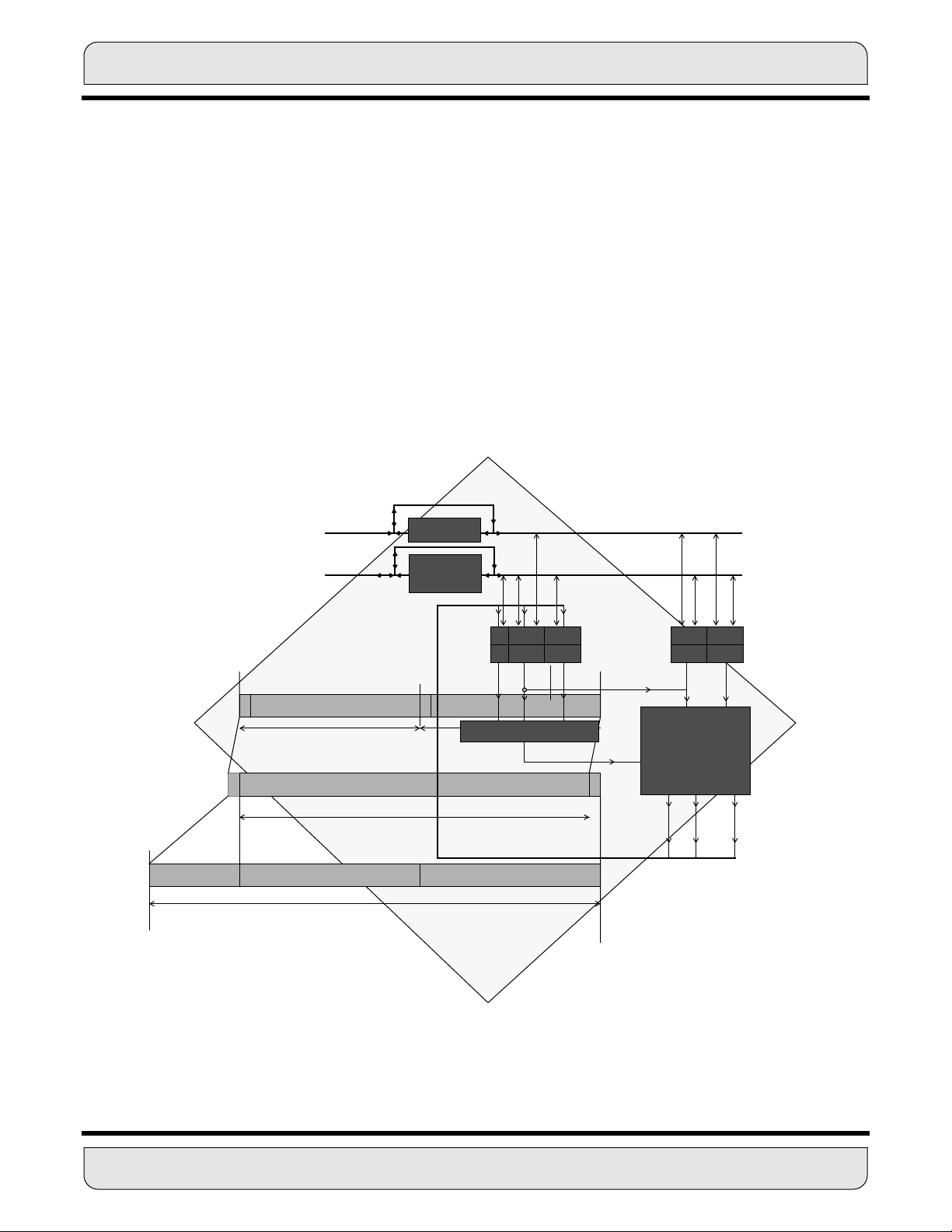
2.1 DSP56K CENTRAL ARCHITECTURE OVERVIEW
The DSP56K family of processors is built on a standard central processing module. In the
expansion area around the central processing module, the chip can support various configurations of memory and peripheral modules which may change from family member to
family member. This section introduces the architecture and the major components of the
central processing module.
The central components are:
• Data Buses
• Address Buses
• Data Arithmetic Logic Unit (data ALU)
• Address Generation Unit (AGU)
• Program Control Unit (PCU)
• Memory Expansion (Port A)
• On-Chip Emulator (OnCE™) circuitry
• Phase-locked Loop (PLL) based clock circuitry
Figure 2-1 shows a block diagram of a typical DSP56K family processor, including the
central processing module and a nonspecific expansion area for memory and peripherals.
The following paragraphs give brief descriptions of each of the central components. Each
of the components is explained in detail in subsequent chapters.
2.2 DATA BUSES
The DSP56K central processing module is organized around the registers of three independent execution units: the PCU, the AGU, and the data ALU. Data movement between
the execution units occurs over four bidirectional 24-bit buses: the X data bus (XDB), the
Y data bus (YDB), the program data bus (PDB), and the global data bus (GDB). (Certain
instructions treat the X and Y data buses as one 48-bit data bus by concatenating them.)
Data transfers between the data ALU and the X data memory or Y data memory occur
over XDB and YDB, respectively. XDB and YDB are kept local on the chip to maximize
speed and minimize power dissipation. All other data transfers, such as I/O transfers with
peripherals, occur over the GDB. Instruction word prefetches occur in parallel over the
PDB.
The bus structure supports general register-to-register, register-to-memory, and memoryto-register data movement. It can transfer up to two 24-bit words and one 56-bit word in
the same instruction cycle. Transfers between buses occur in the internal bus switch.
MOTOROLA DSP56K CENTRAL ARCHITECTURE OVERVIEW 2 - 3
Page 31

PERIPHERAL
PINS
24-Bit 56K
Module
PERIPHERAL
MODULES
ADDRESS
GENERATION
UNIT
ADDRESS BUSES
PROGRAM
RAM/ROM
EXPANSION
X MEMORY
RAM/ROM
EXPANSION
YAB
XAB
PAB
Y MEMORY
RAM/ROM
EXPANSION
EXPANSION
AREA
EXTERNAL
ADDRESS
BUS
SWITCH
ADDRESS
INTERNAL
DATA
BUS
SWITCH
PLL
CLOCK
GENERATOR
PROGRAM
INTERRUPT
CONTROLLER
PROGRAM
DECODE
CONTROLLER
Program Control Unit
MODC/NMI
MODB/IRQB
MODA/IRQA
RESET
PROGRAM
ADDRESS
GENERA TOR
YDB
XDB
PDB
GDB
DATA ALU
24X24+56→56-BIT MAC
TWO 56-BIT ACCUMULATORS
BUS
CONTROL
EXTERNAL
DATA BUS
SWITCH
OnCE™
16 BITS
24 BITS
PORT A
CONTROL
DATA
Figure 2-1 DSP56K Block Diagram
2.3 ADDRESS BUSES
Addresses are specified for internal X data memory and Y data memory on two unidirectional 16-bit buses — X address bus (XAB) and Y address bus (YAB). Program memory
addresses are specified on the bidirectional program address bus (PAB). External mem-
2- 4 DSP56K CENTRAL ARCHITECTURE OVERVIEW
MOTOROLA
Page 32

DATA ALU
ory spaces are addressed over a single 16-bit unidirectional address bus driven by a
three-input multiplexer that can select the XAB, the YAB, or the PAB. Only one external
memory access can be made in an instruction cycle. There is no speed penalty if only one
external memory space is accessed in an instruction cycle. However, if two or three external memory spaces are accessed in a single instruction, there will be a one or two
instruction cycle execution delay, respectively.
A bus arbitrator controls external access.
2.3.1 Internal Bus Switch
Transfers between buses occur in the internal bus switch. The internal bus switch, which
is similar to a switch matrix, can connect any two internal buses without adding any pipeline delays. This flexibility simplifies programming.
2.3.2 Bit Manipulation Unit
The bit manipulation unit is physically located in the internal bus switch block because the
internal data bus switch can access each memory space. The bit manipulation unit performs bit manipulation operations on memory locations, address registers, control
registers, and data registers over the XDB, YDB, and GDB.
2.4 DATA ALU
The data ALU performs all of the arithmetic and logical operations on data operands. It
consists of four 24-bit input registers, two 48-bit accumulator registers, two 8-bit accumulator extension registers, an accumulator shifter, two data bus shifter/limiter circuits, and
a parallel, single-cycle, nonpipelined Multiply-Accumulator (MAC) unit.
2.5 ADDRESS GENERATION UNIT
The AGU performs all of the address storage and address calculations necessary to indirectly address data operands in memory. It operates in parallel with other chip resources
to minimize address generation overhead. The AGU has two identical address arithmetic
units that can generate two 16-bit addresses every instruction cycle. Each of the arithmetic units can perform three types of arithmetic: linear, modulo, and reverse-carry.
2.6 PROGRAM CONTROL UNIT
The program control unit performs instruction prefetch, instruction decoding, hardware
DO loop control, and interrupt (or exception) processing. It consists of three components:
the program address generator, the program decode controller, and the program interrupt
controller. It contains a 15-level by 32-bit system stack memory and the following six di-
MOTOROLA DSP56K CENTRAL ARCHITECTURE OVERVIEW 2 - 5
Page 33

MEMORY EXPANSION PORT (PORT A)
rectly addressable registers: the program counter (PC), loop address (LA), loop counter
(LC), status register (SR), operating mode register (OMR), and stack pointer (SP). The
16-bit PC can address 65,536 locations in program memory space.
There are four mode and interrupt control pins that provide input to the program interrupt
controller. The Mode Select A/External Interrupt Request A(MODA/IRQA
lect B/External Interrupt Request B (MODB/IRQB
and receive interrupt requests from external sources.
) pins select the chip operating mode
) and Mode Se-
The Mode Select C/Non-Maskable Interrupt (MODC/NMI
mode options and non-maskable interrupt input.
The RESET pin resets the chip. When it is asserted, it initializes the chip and places it in
the reset state. When it is deasserted, the chip assumes the operating mode indicated by
the MODA, MODB, and MODC pins.
2.7 MEMORY EXPANSION PORT (PORT A)
Port A synchronously interfaces with a wide variety of memory and peripheral devices
over a common 24-bit data bus. These devices include high-speed static RAMs, slower
memory devices, and other DSPs and MPUs in master/slave configurations. This variety
is possible because the expansion bus timing is programmable and can be tailored to
match the speed requirements of the different memory spaces. Not all DSP56K family
members feature a memory expansion port. See the individual device’s User’s Manual to
determine if a particular chip includes this feature.
2.8 ON-CHIP EMULATOR (OnCE)
DSP56K on-chip emulation (OnCE) circuitry allows the user to interact with the DSP56K
and its peripherals non-intrusively to examine registers, memory, or on-chip peripherals.
It provides simple, inexpensive, and speed independent access to the internal registers
for sophisticated debugging and economical system development.
) pin provides further operating
Dedicated OnCE pins allow the user to insert the DSP into its target system and retain
debug control without sacrificing other user accessible on-chip resources. The design
eliminates the costly cabling and the access to processor pins required by traditional emulator systems.
2.9 PHASE-LOCKED LOOP (PLL) BASED CLOCKING
The PLL allows the DSP to use almost any available external system clock for full-speed
operation, while also supplying an output clock synchronized to a synthesized internal
clock. The PLL performs frequency multiplication, skew elimination, and low-power
division.
2- 6 DSP56K CENTRAL ARCHITECTURE OVERVIEW
MOTOROLA
Page 34
SECTION 3
DATA ARITHMETIC LOGIC UNIT
MOTOROLA DATA ARITHMETIC LOGIC UNIT 3 - 1
Page 35

SECTION CONTENTS
SECTION 3.1 DATA ARITHMETIC LOGIC UNIT .............................................3
SECTION 3.2 OVERVIEW AND DATA ALU ARCHITECTURE .......................3
3.2.1 Data ALU Input Registers (X1, X0, Y1, Y0) ........................................5
3.2.2 MAC and Logic Unit ............................................................................6
3.2.3 Data ALU A and B Accumulators ........................................................7
3.2.4 Accumulator Shifter ............................................................................ 9
3.2.5 Data Shifter/Limiter ............................................................................. 9
3.2.5.1 Limiting (Saturation Arithmetic) .................................................. 9
3.2.5.2 Scaling ........................................................................................ 10
SECTION 3.3 DATA REPRESENTATION AND ROUNDING ..........................10
SECTION 3.4 DOUBLE PRECISION MULTIPLY MODE .................................16
SECTION 3.5 DATA ALU PROGRAMMING MODEL .......................................19
SECTION 3.6 DATA ALU SUMMARY ..............................................................19
3 - 2 DATA ARITHMETIC LOGIC UNIT
MOTOROLA
Page 36

DATA ARITHMETIC LOGIC UNIT
3.1 DATA ARITHMETIC LOGIC UNIT
This section describes the operation of the Data ALU registers and hardware. It discusses data representation, rounding, and saturation arithmetic used within the Data
ALU, and concludes with a discussion of the programming model.
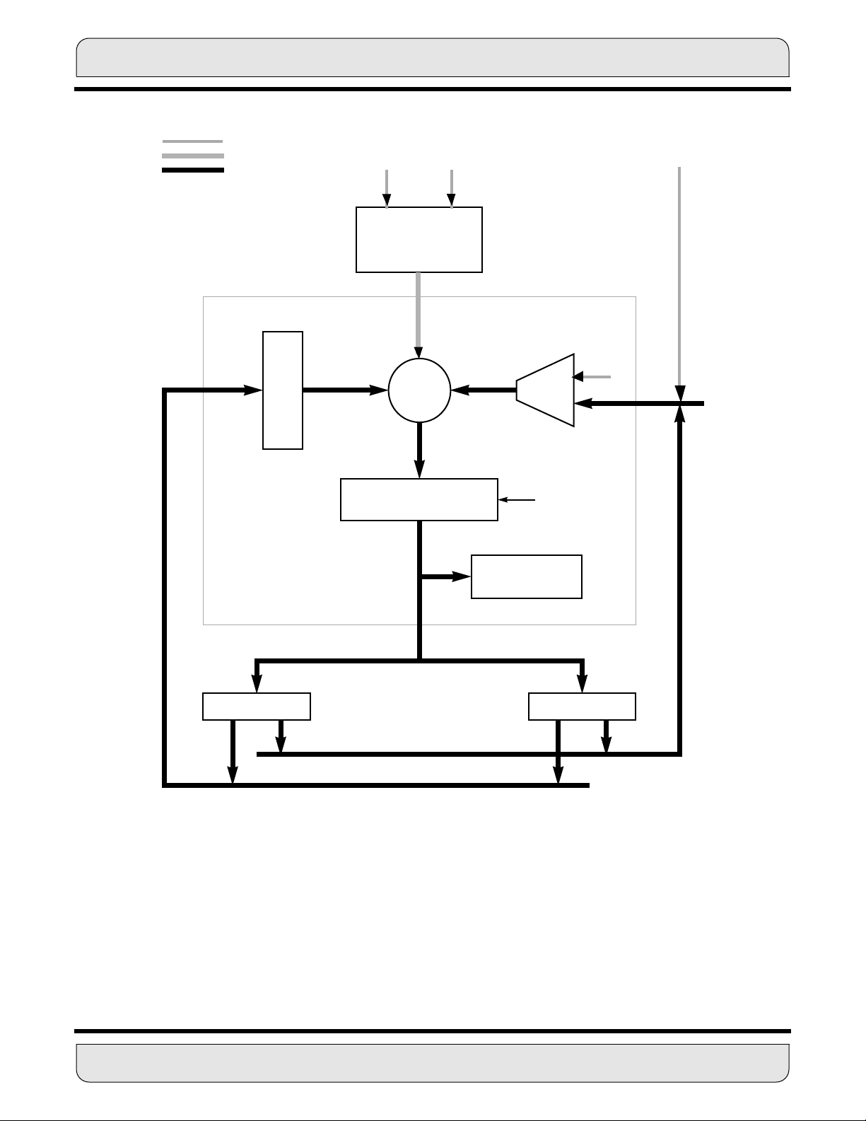
3.2 OVERVIEW AND DATA ALU ARCHITECTURE
As described in Section 2, The DSP56K family central processing module is composed
of three execution units that operate in parallel. They are the Data ALU, address generation unit (AGU), and the program control unit (PCU) (see Figure 3-1). These three units
are register oriented rather than bus oriented and interface over the system buses with
memory and memory-mapped I/O devices.
The Data ALU (see Figure 3-2) is the first of these execution units to be presented. It balances speed with the capability to process signals that have a wide dynamic range and
performs all arithmetic and logical operations on data operands.
The Data ALU registers may be read or written over the XDB and the YDB as 24- or 48bit operands. The source operands for the Data ALU, which may be 24, 48, or 56 bits,
always originate from Data ALU registers. The results of all Data ALU operations are
stored in an accumulator.
The 24-bit data words provide 144 dB of dynamic range. This range is sufficient for most
real-world applications since the majority of data converters are 16 bits or less – and certainly not greater than 24 bits. The 56-bit accumulator inside the Data ALU provides 336
dB of internal dynamic range so that no loss of precision will occur due to intermediate
processing. Special circuitry handles data overflows and roundoff errors.
The Data ALU can perform any of the following operations in a single instruction cycle:
multiplication, multiply-accumulate with positive or negative accumulation, convergent
rounding, multiply-accumulate with positive or negative accumulation and convergent
rounding, addition, subtraction, a divide iteration, a normalization iteration, shifting, and
logical operations.
The components of the Data ALU are:
• Four 24-bit input registers
• A parallel, single-cycle, nonpipelined multiply-accumulator/logic unit (MAC)
• Two 48-bit accumulator registers
• Two 8-bit accumulator extension registers
• An accumulator shifter
• Two data bus shifter/limiter circuits
MOTOROLA DATA ARITHMETIC LOGIC UNIT 3 - 3
Page 37

PERIPHERAL
PINS
24 Bit 56K
Module
OVERVIEW AND DATA ALU ARCHITECTURE
PERIPHERAL
MODULES
ADDRESS
GENERATION
UNIT
PROGRAM
RAM/ROM
EXPANSION
YAB
XAB
PAB
X MEMORY
RAM/ROM
EXPANSION
Y MEMORY
RAM/ROM
EXPANSION
EXPANSION
AREA
EXTERNAL
ADDRESS
BUS
SWITCH
ADDRESS
INTERNAL
DATA
BUS
SWITCH
PLL
CLOCK
GENERATOR
PROGRAM
INTERRUPT
CONTROLLER
PROGRAM
DECODE
CONTROLLER
Program Control Unit
MODC/NMI
MODB/IRQB
MODA/IRQA
RESET
PROGRAM
ADDRESS
GENERA TOR
YDB
XDB
PDB
GDB
DATA ALU
24X24+56→56-BIT MAC
TWO 56-BIT ACCUMULATORS
BUS
CONTROL
EXTERNAL
DATA BUS
SWITCH
OnCE™
16 BITS
24 BITS
PORT A
CONTROL
DATA
Figure 3-1 DSP56K Block Diagram
The following paragraphs describe each of these components and provide a description
of data representation, rounding, and saturation arithmetic.
3 - 4 DATA ARITHMETIC LOGIC UNIT
MOTOROLA
Page 38

OVERVIEW AND DATA ALU ARCHITECTURE
3.2.1 Data ALU Input Registers (X1, X0, Y1, Y0)
X1, X0, Y1, and Y0 are four 24-bit, general-purpose data registers. They can be treated
as four independent, 24-bit registers or as two 48-bit registers called X and Y, developed
by concatenating X1:X0 and Y1:Y0, respectively. X1 is the most significant word in X and
Y1 is the most significant word in Y. The registers serve as input buffer registers between
the XDB or YDB and the MAC unit. They act as Data ALU source operands and allow
new operands to be loaded for the next instruction while the current instruction uses the
X DATA BUS
Y DATA BUS
2424
X0
X1
Y0
Y1
56
SHIFTER
24 24
MULTIPLIER
ACCUMULATOR,
ROUNDING,
AND LOGIC UNIT
56
A (56)
B (56)
5656
SHIFTER/LIMITER
56
24
24
Figure 3-2 Data ALU
MOTOROLA DATA ARITHMETIC LOGIC UNIT 3 - 5
Page 39

OVERVIEW AND DATA ALU ARCHITECTURE
register contents. The registers may also be read back out to the appropriate data bus to
implement memory-delay operations and save/restore operations for interrupt service
routines.
3.2.2 MAC and Logic Unit
The MAC and logic unit shown in Figure 3-3 conduct the main arithmetic processing and
perform all calculations on data operands in the DSP.
For arithmetic instructions, the unit accepts up to three input operands and outputs one
56-bit result in the following form: extension:most significant product:least significant
product (EXT:MSP:LSP). The operation of the MAC unit occurs independently and in parallel with XDB and YDB activity, and its registers facilitate buffering for Data ALU inputs
and outputs. Latches on the MAC unit input permit writing an input register which is the
source for a Data ALU operation in the same instruction.
The arithmetic unit contains a multiplier and two accumulators. The input to the multiplier
can only come from the X or Y registers (X1, X0, Y1, Y0). The multiplier executes 24-bit
x 24-bit, parallel, twos-complement fractional multiplies. The 48-bit product is right justified and added to the 56-bit contents of either the A or B accumulator. The 56-bit sum is
stored back in the same accumulator (see Figure 3-3). An 8-bit adder, which acts as an
extension accumulator for the MAC array, accommodates overflow of up to 256 and allows the two 56-bit accumulators to be added to and subtracted from each other. The
extension adder output is the EXT portion of the MAC unit output. This multiply/accumulate operation is not pipelined, but is a single-cycle operation. If the instruction specifies a
multiply without accumulation (MPY), the MAC clears the accumulator and then adds the
contents to the product.
In summary, the results of all arithmetic instructions are valid (sign-extended and zerofilled) 56-bit operands in the form of EXT:MSP:LSP (A2:A1:A0 or B2:B1:B0). When a 56bit result is to be stored as a 24-bit operand, the LSP can be simply truncated, or it can be
rounded (using convergent rounding) into the MSP.
Convergent rounding (round-to-nearest) is performed when the instruction (for example,
the signed multiply-accumulate and round (MACR) instruction) specifies adding the multiplier’s product to the contents of the accumulator. The scaling mode bits in the status
register specify which bit in the accumulator shall be rounded.
The logic unit performs the logical operations AND, OR, EOR, and NOT on Data ALU registers. It is 24 bits wide and operates on data in the MSP portion of the accumulator. The
LSP and EXT portions of the accumulator are not affected.
3 - 6 DATA ARITHMETIC LOGIC UNIT
MOTOROLA
Page 40
OVERVIEW AND DATA ALU ARCHITECTURE
24 BITS
48 BITS
56 BITS
X0,X1,
Y0, OR Y1
24-BITx24-BIT
FRACTIONAL
MULTIPLIER
S
H
I
F
T
E
R
CONVERGENT - ROUNDING
FORCING FUNCTION
X0,X1,
Y0, OR Y1
+
–
56 - BIT
ARITHMETIC AND
LOGIC UNIT
SCALING
MODE BITS
R
X0,X1,
Y0, OR Y1
24
CONDITION
CODE GENERATOR
ACCUMULATOR A ACCUMULATOR B
Figure 3-3 MAC Unit
3.2.3 Data ALU A and B Accumulators
The Data ALU features two general-purpose, 56-bit accumulators, A and B. Each consists of three concatenated registers (A2:A1:A0 and B2:B1:B0, respectively). The 8-bit
sign extension (EXT) is stored in A2 or B2 and is used when more than 48-bit accuracy is
needed; the 24-bit most significant product (MSP) is stored in A1 or B1; the 24-bit least
MOTOROLA DATA ARITHMETIC LOGIC UNIT 3 - 7
Page 41

OVERVIEW AND DATA ALU ARCHITECTURE
DATA ALU ACCUMULATOR REGISTERS
Accumulator A
A2 A1 A0
*
7023 023 0
Accumulator B
55 055 0
B2
*
7023 023 0
B1 B0
EXT MSP LSP
*Read as sign extension bits, written as don’t care.
EXT MSP LSP
Figure 3-4 DATA ALU Accumulator Registers
significant product (LSP) is stored in A0 or B0 as shown in Figure 3-4.
Overflow occurs when a source operand requires more bits for accurate representation
than are available in the destination. The 8-bit extension registers offer protection
against overflow. In the DSP56K chip family, the extreme values that a word operand
can assume are - 1 and + 0.9999998. If the sum of two numbers is less than - 1 or
greater than + 0.9999998, the result (which cannot be represented in a 24 bit word operand) has underflowed or overflowed. The 8-bit extension registers can accurately represent the result of 255 overflows or 255 underflows. Whenever the accumulator extension
registers are in use, the V bit in the status register is set.
Automatic sign extension occurs when the 56-bit accumulator is written with a smaller
operand of 48 or 24 bits. A 24-bit operand is written to the MSP (A1 or B1) portion of the
accumulator, the LSP (A0 or B0) portion is zero filled, and the EXT (A2 or B2) portion is
sign extended from MSP. A 48-bit operand is written into the MSP:LSP portion (A1:A0 or
B1:B0) of the accumulator, and the EXT portion is sign extended from MSP. No sign
extension occurs if an individual 24-bit register is written (A1, A0, B1, or B0).When either
A or B is read, it may be optionally scaled one bit left or one bit right for block floatingpoint arithmetic. Sign extension can also occur when writing A or B from the XDB and/or
YDB or with the results of certain Data ALU operations (such as the transfer conditionally
(Tcc) or transfer Data ALU register (TFR) instructions).
Overflow protection occurs when the contents of A or B are transferred over the XDB and
YDB by substituting a limiting constant for the data. Limiting does not affect the content
of A or B – only the value transferred over the XDB or YDB is limited. This overflow protection occurs after the contents of the accumulator has been shifted according to the
scaling mode. Shifting and limiting occur only when the entire 56-bit A or B accumulator
is specified as the source for a parallel data move over the XDB or YDB. When individual
registers A0, A1, A2, B0, B1, or B2 are specified as the source for a parallel data move,
3 - 8 DATA ARITHMETIC LOGIC UNIT
MOTOROLA
Page 42

OVERVIEW AND DATA ALU ARCHITECTURE
shifting and limiting are not performed.
3.2.4 Accumulator Shifter
The accumulator shifter (see Figure 3-3) is an asynchronous parallel shifter with a 56-bit
input and a 56-bit output that is implemented immediately before the MAC accumulator
input. The source accumulator shifting operations are as follows:
• No Shift (Unmodified)
• 1-Bit Left Shift (Arithmetic or Logical) ASL, LSL, ROL
• 1-Bit Right Shift (Arithmetic or Logical) ASR, LSR, ROR
• Force to zero
3.2.5 Data Shifter/Limiter
The data shifter/limiter circuits (see Figure 3-3) provide special post-processing on data
read from the Data ALU A and B accumulators out to the XDB or YDB. There are two independent shifter/limiter circuits (one for XDB and one for the YDB); each consists of a
shifter followed by a limiting circuit.
3.2.5.1 Limiting (Saturation Arithmetic)
The A and B accumulators serve as buffer registers between the MAC unit and the XDB
and/or YDB. They act both as Data ALU source and destination operands.Test logic exists
in each accumulator register to support the operation of the data shifter/limiter circuits.
This test logic detects overflows out of the data shifter so that the limiter can substitute
one of several constants to minimize errors due to the overflow. This process is called saturation arithmetic
The Data ALU A and B accumulators have eight extension bits. Limiting occurs when the
extension bits are in use and either A or B is the source being read over XDB or YDB. If
the contents of the selected source accumulator can be represented without overflow in
the destination operand size (i.e., accumulator extension register not in use), the data limiter is disabled, and the operand is not modified. If contents of the selected source
accumulator cannot be represented without overflow in the destination operand size, the
data limiter will substitute a limited data value with maximum magnitude (saturated) and
with the same sign as the source accumulator contents: $7FFFFF for 24-bit or $7FFFFF
FFFFFF for 48-bit positive numbers, $800000 for 24-bit or $800000 000000 for 48-bit negative numbers. This process is called saturation arithmetic. The value in the accumulator
register is not shifted and can be reused within the Data ALU. When limiting does occur,
a flag is set and latched in the status register.Two limiters allow two-word operands to be
limited independently in the same instruction cycle. The two data limiters can also be com-
MOTOROLA DATA ARITHMETIC LOGIC UNIT 3 - 9
Page 43
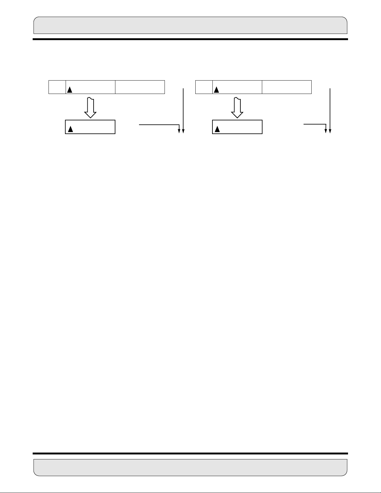
DATA REPRESENTATION AND ROUNDING
WITHOUT LIMITING* WITH LIMITING*
55 0
0 . . . 0 1 0 0 . . . . . . . . . . . 0 0 0 0 . . . . . . . . . . . . 0 0
7 0 23 0 23 0
MOVE A1, X0
1 0 0 . . . . . . . . . . . 0 0 0 1 1 . . . . . . . . . . . 1 1
23 0 23 0
* Limiting automatically occurs when the 56 - bit operands A or B (not A2, A1, A0, B2, B1, or B0) are read. The contents
of A or B are NOT changed.
X0 = -1.0 X0 = +0.9999999
A = +1.0
|ERROR| = 2.0
55 0
0. . . 0 1 0 0 . . . . . . . . . . . 0 0 0 0 . . . . . . . . . . . . 0 0
7 0 23 0 23 0
MOVE A, X0
|ERROR| = .0000001
A = +1.0
Figure 3-5 Saturation Arithmetic
bined to form one 48-bit data limiter for long-word operands.
For example, if the source operand were 01.100 (+ 1.5 decimal) and the destination reg-
ister were only four bits, the destination register would contain 1.100 (- 1.5 decimal) after
the transfer, assuming signed fractional arithmetic. This is clearly in error as overflow has
occurred. To minimize the error due to overflow, it is preferable to write the maximum
(“limited”) value the destination can assume. In the example, the limited value would be
0.111 (+ 0.875 decimal), which is clearly closer to + 1.5 than - 1.5 and therefore introduces less error.
Figure 3-5 shows the effects of saturation arithmetic on a move from register A1 to register X0. The instruction “MOVE A1,X0” causes a move without limiting, and the instruction
“MOVE A,X0” causes a move of the same 24 bits with limiting. The error without limiting
is 2.0; whereas, it is 0.0000001 with limiting. Table 3-1 shows a more complete set of
limiting situations.
3.2.5.2 Scaling
The data shifters can shift data one bit to the left or one bit to the right, or pass the data
unshifted. Each data shifter has a 24-bit output with overflow indication and is controlled
by the scaling mode bits in the status register. These shifters permit dynamic scaling of
fixed-point data without modifying the program code. For example, this permits block
floating-point algorithms such as fast Fourier transforms to be implemented in a regular
fashion.
3.3 DATA REPRESENTATION AND ROUNDING
The DSP56K uses a fractional data representation for all Data ALU operations. Figure 3-
3 - 10 DATA ARITHMETIC LOGIC UNIT
MOTOROLA
Page 44
DATA REPRESENTATION AND ROUNDING
Table 3-1 Limited Data Values
Destination
Memory Reference
X
Y
X and Y
L (X:Y)
Source
Operand
X:A
X:B
Y:A
Y:B
X:A Y:A
X:A Y:B
X:B Y:A
X:B Y:B
L:AB
L:BA
L:A
L:B
Accumulator
Sign
+
-
+
-
+
-
+
-
+
+
-
Limited Value (Hexadecimal) Type of
XDB YDB
7FFFFF
800000
—
—
7FFFFF
800000
7FFFFF
800000
7FFFFF
800000
7FFFFF
800000
7FFFFF
800000
7FFFFF
800000
7FFFFF
800000
7FFFFF
800000
FFFFFF
000000
—
—
Access
One 24 bit
One 24 bit
Two 24 bit
One 48 bit
7 shows the bit weighting of words, long words, and accumulator operands for this representation. The decimal points are all aligned and are left justified.
Data must be converted to a fractional number by scaling before being used by the DSP
or the user will have to be very careful in how the DSP manipulates the data. Moving $3F
to a 24-bit Data ALU register does not result in the contents being $00003F as might be
expected. Assuming numbers are fractional, the DSP left justifies rather than right justifies. As a result, storing $3F in a 24-bit register results in the contents being $3F0000.
The simplest example of scaling is to convert all integer numbers to fractional numbers
by shifting the decimal 24 places to the left (see Figure 3-6). Thus, the data has not
changed; only the position of the decimal has moved.
S3F.
S.3F
S = SIGN BIT
3F = HEXADECIMAL DATA TO BE CONVERTED
Figure 3-6 Integer-to-Fractional Data Conversion
For words and long words, the most negative number that can be represented is -1
whose internal representation is $800000 and $800000000000, respectively. The most
positive word is $7FFFFF or 1 - 2
-23
and the most positive long word is $7FFFFFFFFFFF
MOTOROLA DATA ARITHMETIC LOGIC UNIT 3 - 11
Page 45

DATA REPRESENTATION AND ROUNDING
or 1 - 2
-47
. These limitations apply to all data stored in memory and to data stored in the
Data ALU input buffer registers. The extension registers associated with the accumulators allow word growth so that the most positive number that can be used is approximately 256 and the most negative number is approximately -256. When the accumulator
extension registers are in use, the data contained in the accumulators cannot be stored
exactly in memory or other registers. In these cases, the data must be limited to the most
positive or most negative number consistent with the size of the destination and the sign
of the accumulator (the most significant bit (MSB) of the extension register).
To maintain alignment of the binary point when a word operand is written to accumulator
A or B, the operand is written to the most significant accumulator register (A1 or B1), and
its MSB is automatically sign extended through the accumulator extension register. The
least significant accumulator register is automatically cleared. When a long-word operand is written to an accumulator, the least significant word of the operand is written to the
least significant accumulator register A0 or B0 and the most significant word is written to
DATA ALU
–2
0
–23
2
WORD OPERAND
X1, X0
Y1, Y0
A1, A0
B1, B0
LONG - WORD OPERAND
X1:X0 = X
Y1:Y0 = Y
A1:A0 = A10
B1:B0 = B10
ACCUMULATOR A OR B
Figure 3-7 Bit Weighting and Alignment of Operands
–2
0
–24
2
*
8
–2
A2, B2 A1, B1 A0, B0
SIGN EXTENSION OPERAND ZERO
0
2
–24
2
–47
2
–47
2
3 - 12 DATA ARITHMETIC LOGIC UNIT
MOTOROLA
Page 46

DATA REPRESENTATION AND ROUNDING
A1 or B1(see Figure 3-8).
TWOS COMPLEMENT INTEGER
N BITS
S
(N–1)
–2
•
TO [+2
(N–1)
–1]
TWOS COMPLEMENT FRACTIONAL
FRACTIONAL = INTEGER EXCEPT FOR X AND
÷
S
•
N BITS
–1 TO [+1–2
–(N–1)
]
Figure 3-8 Integer/Fractional Number Comparison
A comparison between integer and fractional number representation is shown in Figure
. The number representation for integers is between ± 2
3-8
(N-1)
; whereas, the fractional
representation is limited to numbers between ± 1. To convert from an integer to a fractional number, the integer must be multiplied by a scaling factor so the result will always
be between ± 1. The representation of integer and fractional numbers is the same if the
numbers are added or subtracted but is different if the numbers are multiplied or divided.
An example of two numbers multiplied together is given in Figure 3-9. The key difference
is that the extra bit in the integer multiplication is used as a duplicate sign bit and as the
least significant bit (LSB) in the fractional multiplication. The advantages of fractional
data representation are as follows:
• The MSP (left half) has the same format as the input data.
• The LSP (right half) can be rounded into the MSP without shifting or updating the
exponent.
• A significant bit is not lost through sign extension.
• Conversion to floating-point representation is easier because the industry-standard
floating-point formats use fractional mantissas.
• Coefficients for most digital filters are derived as fractions by the high-level language
programs used in digital-filter design packages, which implies that the results can be
used without the extensive data conversions that other formats require.
Should integer arithmetic be required in an application, shifting a one or zero, depending
on the sign, into the MSB converts a fraction to an integer.
The Data ALU MAC performs rounding of the accumulator register to single precision if
requested in the instruction (the A1 or B1 register is rounded according to the contents of
the A0 or B0 register). The rounding method is called round-to-nearest (even) number, or
convergent rounding. The usual rounding method rounds up any value above one-half
MOTOROLA DATA ARITHMETIC LOGIC UNIT 3 - 13
Page 47

DATA REPRESENTATION AND ROUNDING
SIGNED MULTIPLICATION N x N - 2N – 1 BITS
INTEGER FRACTIONAL
S S
SIGNED MULTIPLIER
.
S
S MSP LSP •
2N — 1 PRODUCT
SIGN EXTENSION
.
.
2N BITS
S S
SIGNED MULTIPLIER
.
S• MSP LSP
2N — 1 PRODUCT
.
.
2N BITS
0
ZERO FILL
Figure 3-9 Integer/Fractional Multiplication Comparison
and rounds down any value below one-half. The question arises as to which way onehalf should be rounded. If it is always rounded one way, the results will eventually be
biased in that direction. Convergent rounding solves the problem by rounding down if the
number is odd (LSB=0) and rounding up if the number is even (LSB=1). Figure 3-10
shows the four cases for rounding a number in the A1 (or B1) register. If scaling is set in
the status register, the resulting number will be rounded as it is put on the data bus. However, the contents of the register are not scaled.
3 - 14 DATA ARITHMETIC LOGIC UNIT
MOTOROLA
Page 48

DATA REPRESENTATION AND ROUNDING
CASE I: IF A0 < $800000 (1/2), THEN ROUND DOWN (ADD NOTHING)
BEFORE ROUNDING
0
A2 A1 A0
XX . .XX XXX . . .XXX0100 011XXX . . . . XXX
55 48 47 24 23 0
CASE II: IF A0 > $800000 (1/2), THEN ROUND UP (ADD 1 TO A1)
BEFORE ROUNDING
1
A2 A1 A0
XX . .XX XXX . . .XXX0100 1110XX . . . . XXX
55 48 47 24 23 0
CASE III: IF A0 = $800000 (1/2), AND THE LSB OF A1 = 0,THEN ROUND DOWN (ADD NOTHING)
BEFORE ROUNDING
0
A2 A1 A0
XX . .XX XXX . . . XXX0100 10000 . . . . . . 000
55 48 47 24 23 0
AFTER ROUNDING
A2 A1 A0*
XX . . XX XXX . . . XXX0100 000 . . . . . . . . 000
55 48 47 24 23 0
AFTER ROUNDING
A2 A1 A0*
XX . .XX XXX . . . XXX0101 000 . . . . . . . . 000
55 48 47 24 23 0
AFTER ROUNDING
A2 A1 A0*
XX . .XX XXX . . . XXX0100 000 . . . . . . . . 000
55 48 47 24 23 0
CASE IV: IF A0 = $800000 (1/2), AND THE LSB = 1, THEN ROUND UP (ADD 1 TO A1)
BEFORE ROUNDING
1
A2 A1 A0
XX . .XX XXX . . .XXX0101 10000 . . . . . . 000
55 48 47 24 23 0
*A0 is always clear; performed during RND, MPYR, MACR
AFTER ROUNDING
A2 A1 A0*
XX . .XX XXX . . .XXX0110 000 . . . . . . . . 000
55 48 47 24 23 0
Figure 3-10 Convergent Rounding
MOTOROLA DATA ARITHMETIC LOGIC UNIT 3 - 15
Page 49

DOUBLE PRECISION MULTIPLY MODE
3.4 DOUBLE PRECISION MULTIPLY MODE
The Data ALU double precision multiply operation multiplies two 48-bit operands with a
96-bit result. The processor enters the dedicated Double Precision Multiply Mode when
the user sets bit 14 (DM) of the Status Register (bit 6 of the MR register). The mode is
disabled by clearing the DM bit. For information on the DM bit, see Section 5.4.2.13 Double Precision Multiply Mode (Bit 14).
CAUTION:
While in the Double Precision Multiply Mode, only the double precision m ultiply algorithms
shown in Figure 3-11, Figure 3-12, and Figure 3-13 may be executed by the Data ALU;
any other Data ALU operation will give indeterminate results.
Figure 3-11 shows the full double precision multiply algorithm. To allow for pipeline
delay, the ANDI instruction should not be immediately followed by a Data ALU instruction. For example, the ORI instruction sets the DM mode bit, but, due to the instruction
execution pipeline, the Data ALU enters the Double Precision Multiply mode only after
Y:X:
MSP2
LSP2
DP2
DP0
R5
R0
R1
R0
MSP1
LSP1
DP3
DP1
DP3_DP2_DP1_DP0 = MSP1_LSP1 x MSP2_LSP2
ori #$40,mr ;enter mode
move x:(r1)+,x0 y:(r5)+,y0 ;load operands
mpy y0,x0,a x:(r1)+,x1 y:(r5)+,y1 ;LSP*LSP➞a
mac x1,y0,a a0,y:(r0) ;shifted(a)+
; MSP*LSP➞a
mac x0,y1,a ;a+LSP*MSP➞a
mac y1,x1,a a0,x:(r0)+ ;shifted(a)+
; MSP*MSP➞a
move a,l:(r0)+
andi #$bf,mr ;exit mode
non-Data ALU operation ;pipeline delay
Figure 3-11 Full Double Precision Multiply Algorithm
3 - 16 DATA ARITHMETIC LOGIC UNIT
MOTOROLA
Page 50

DOUBLE PRECISION MULTIPLY MODE
one instruction cycle. The ANDI instruction clears the DM mode bit, but, due to the
instruction execution pipeline, the Data ALU leaves the mode after one instruction cycle.
The double precision multiply algorithm uses the Y0 register at all stages. If the use of
the Data ALU is required in an interrupt service routine, Y0 should be saved together
with other Data ALU registers to be used, and should be restored before leaving the
interrupt routine.
If just single precision times double precision multiply is desired, two of the multiply operations may be deleted and replaced by suitable initialization and clearing of the accumulator and Y0. Figure 3-12 shows the single precision times double precision algorithm.
Y:X:
R5
R0
R1
R0
SPMSP1
LSP1
DP2DP3
DP1
DP3_DP2_DP1 = MSP1_LSP1 x SP
clr a #0,y0 ;clear a and y0
ori #$40,mr ;enter DP mode
move x:(r1)+,x0 y:(r5)+,y1 ;load LSP1 and SP
mac x0,y1,a x:(r1)+,x1 ;LSP1*SP➞a,
;load MSP1
mac y1,x1,a a0,x:(r0)+ ;shifted(a)+
; SP*MSP1➞a,
;save DP1
move a,l:(r0)+ ;save DP3_DP2
andi #$bf,mr ;exit DP mode
non-Data ALU operation ;pipeline delay
Figure 3-12 Single × Double Multiply Algorithm
Figure 3-13 shows a single precision times double precision multiply-accumulate algorithm. First, the least significant parts of the double precision values are multiplied by the
single precision values and accumulated in the “Double Precision Multiply” mode. Then
the DM bit is cleared and the least significant part of the result is saved to memory. The
most significant parts of the double precision values are then multiplied by the single pre-
MOTOROLA DATA ARITHMETIC LOGIC UNIT 3 - 17
Page 51

DOUBLE PRECISION MULTIPLY MODE
cision values and accumulated using regular MAC instructions. Note that the maximum
number of single times double MAC operations in this algorithm are limited to 255 since
overflow may occur (the A2 register is just eight bits long). If a longer sequence is
required, it should be split into sub-sequences each with no more than 255 MAC operations.
Y:X:
SPiMSPi
R1
R0
DP3_DP2_DP1 =
move #N-1,m5
clr a #0,y0 ;clear a and y0
ori #$40,mr ;enter DP mode
move x:(r1)+,x0 y:(r5)+,y1 ;load LSPi and SPi
rep #N ;0<N<256
mac x0,y1,a x:(r1)+,x0 y:(r5)+,y1 ;LSPi*SPi➞a
andi #$bf,mr ;exit DP mode
move a0,x:(r0)+ ;save DP1
move a1,y0
move a2,a
move y0,a0 ;a2:a1➞a1:a0
rep #N
mac x0,y1,a x:(r1)+,x0 y:(r5)+,y1 ;load MSPi and SPi
move a,l:(r0)+ ;save DP3_DP2
LSPi
DP3
DP1
DP2
∑ MSPi_LSPi x SPi
R5
R0
Figure 3-13 Single × Double Multiply-Accumulate Algorithm
3 - 18 DATA ARITHMETIC LOGIC UNIT MOTOROLA
Page 52

DATA ALU PROGRAMMING MODEL
3.5 DATA ALU PROGRAMMING MODEL
The Data ALU features 24-bit input/output data registers that can be concatenated to accommodate 48-bit data and two 56-bit accumulators, which are segmented into three 24bit pieces that can be transferred over the buses. Figure 3-14 illustrates how the registers
in the programming model are grouped.
DATA ALU
INPUT REGISTERS
X Y
47 0
X1
23 0 23 0
A
A2 A1 A0
*
23 8 7 0 23 0 23 0
*Read as sign extension bits, written as don’t care.
X0
DATA ALU
ACCUMULATOR REGISTERS
55 055 0
*
23 8 7 0 23 0 23 0
47 0
Y1 Y0
23 0 23 0
B
B2
B1 B0
Figure 3-14 DSP56K Programming Model
3.6 DATA ALU SUMMARY
The Data ALU performs arithmetic operations involving multiply and accumulate operations. It executes all instructions in one machine cycle and is not pipelined. The two 24-bit
numbers being multiplied can come from the X registers (X0 or X1) or Y registers (Y0 or
Y1). After multiplication, they are added (or subtracted) with one of the 56-bit accumulators and can be convergently rounded to 24 bits. The convergent-rounding forcing
function detects the $800000 condition in the LSP and makes the correction as necessary. The final result is then stored in one of the accumulators as a valid 56-bit number.
The condition code bits are set based on the rounded output of the logic unit.
MOTOROLA DATA ARITHMETIC LOGIC UNIT 3 - 19
Page 53

DATA ALU SUMMARY
3 - 20 DATA ARITHMETIC LOGIC UNIT MOTOROLA
Page 54
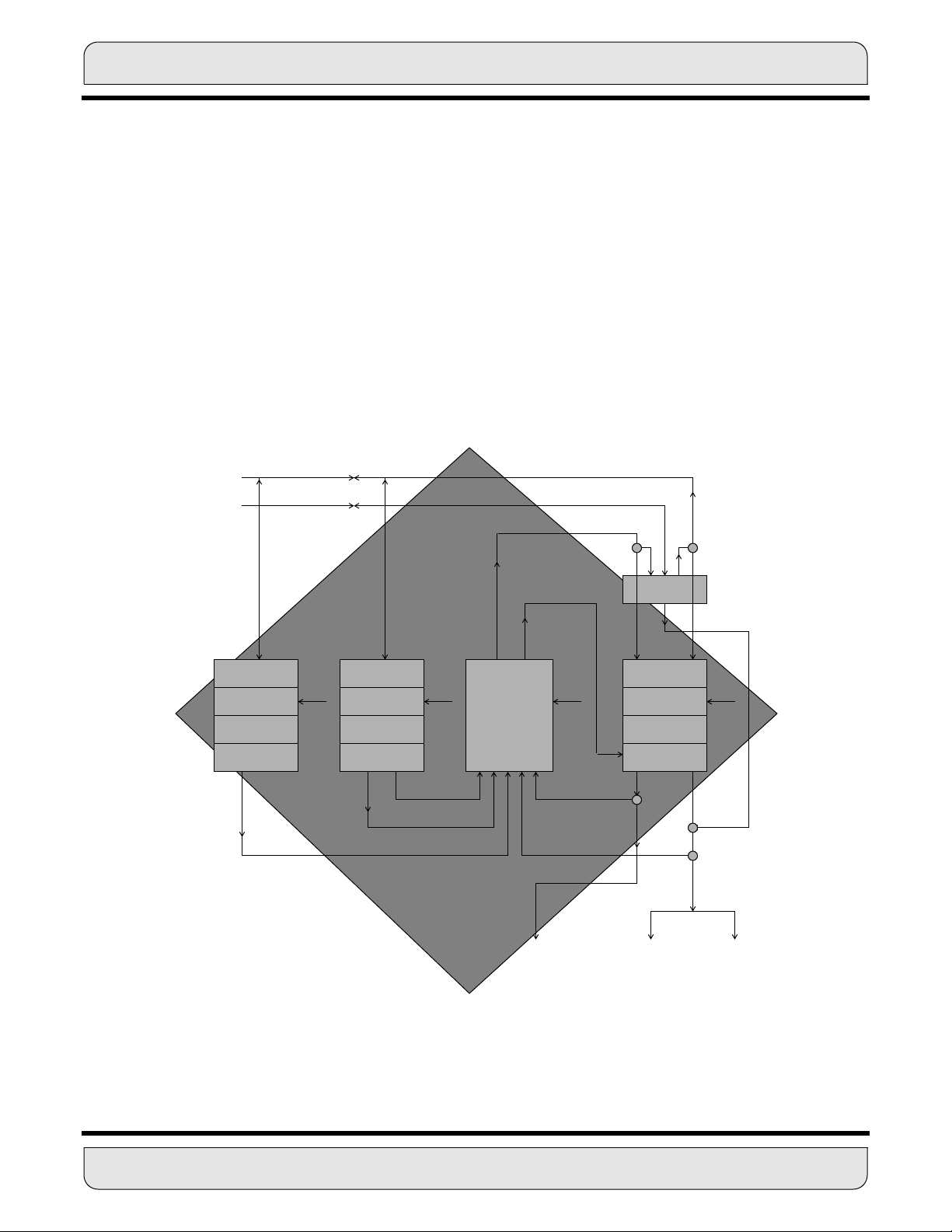
SECTION 4
ADDRESS GENERATION UNIT
MOTOROLA ADDRESS GENERATION UNIT 4 - 1
Page 55

SECTION CONTENTS
SECTION 4.1 ADDRESS GENERATION UNIT AND ADDRESSING MODES ....3
SECTION 4.2 AGU ARCHITECTURE ..................................................................3
4.2.1 Address Register Files (Rn) ................................................................3
4.2.2 Offset Register Files (Nn) ....................................................................4
4.2.3 Modifier Register Files (Mn) ................................................................5
4.2.4 Address ALU .......................................................................................5
4.2.5 Address Output Multiplexers ...............................................................6
SECTION 4.3 PROGRAMMING MODEL .............................................................6
4.3.1 Address Register Files (R0 - R3 and R4 - R7) ....................................7
4.3.2 Offset Register Files (N0 - N3 and N4 - N7) .......................................7
4.3.3 Modifier Register Files (M0 - M3 and M4 - M7) ...................................8
SECTION 4.4 ADDRESSING ...............................................................................8
4.4.1 Address Register Indirect Modes ........................................................9
4.4.1.1 No Update ...................................................................................9
4.4.1.2 Postincrement By 1 .....................................................................9
4.4.1.3 Postdecrement By 1 ...................................................................9
4.4.1.4 Postincrement By Offset Nn .......................................................10
4.4.1.5 Postdecrement By Offset Nn ......................................................11
4.4.1.6 Indexed By Offset Nn ..................................................................12
4.4.1.7 Predecrement By 1 .....................................................................13
4.4.2 Address Modifier Arithmetic Types .....................................................14
4.4.2.1 Linear Modifier (Mn=$FFFF) .......................................................16
4.4.2.2 Modulo Modifier ..........................................................................18
4.4.2.3 Reverse-Carry Modifier (Mn=$0000) ..........................................22
4.4.2.4 Address-Modifier-Type Encoding Summary ...............................25
4 - 2 ADDRESS GENERATION UNIT
MOTOROLA
Page 56

ADDRESS GENERATION UNIT AND ADDRESSING MODES
4.1 ADDRESS GENERATION UNIT AND ADDRESSING MODES
This section contains three major subsections. The first subsection describes the hardware architecture of the address generation unit (AGU), the second subsection
describes the programming model, and the third subsection describes the addressing
modes, explaining how the Rn, Nn, and Mn registers work together to form a memory
address.
4.2 AGU ARCHITECTURE
The AGU is shown in the DSP56K block diagram in Figure 4-1. It uses integer arithmetic
to perform the effective address calculations necessary to address data operands in
memory, and contains the registers used to generate the addresses. It implements linear, modulo, and reverse-carry arithmetic, and operates in parallel with other chip
resources to minimize address-generation overhead.
The AGU is divided into two identical halves, each of which has an address arithmetic
logic unit (ALU) and four sets of three registers (see Figure 4-2). They are the address
registers (R0 - R3 and R4 - R7), offset registers (N0 - N3 and N4 - N7), and the modifier
registers (M0 - M3 and M4 - M7). The eight Rn, Nn, and Mn registers are treated as register triplets — e.g., only N2 and M2 can be used to update R2. The eight triplets are
R0:N0:M0, R1:N1:M1, R2:N2:M2, R3:N3:M3, R4:N4:M4, R5:N5:M5, R6:N6:M6, and
R7:N7:M7.
The two arithmetic units can generate two 16-bit addresses every instruction cycle — one
for any two of the XAB, YAB, or PAB. The AGU can directly address 65,536 locations on
the XAB, 65,536 locations on the YAB, and 65,536 locations on the PAB. The two independent address ALUs work with the two data memories to feed the data ALU two
operands in a single cycle. Each operand may be addressed by an Rn, Nn, and Mn triplet.
4.2.1 Address Register Files (Rn)
Each of the two address register files (see Figure 4-2) consists of four 16-bit registers. The
two files contain address registers R0 - R3 and R4 - R7, which usually contain addresses
used as pointers to memory. Each register may be read or written by the global data bus
(GDB). When read by the GDB, 16-bit registers are written into the two least significant
bytes of the GBD, and the most significant byte is set to zero. When written from the GBD,
only the two least significant bytes are written, and the most significant byte is truncated.
Each address register can be used as input to its associated address ALU for a register
update calculation. Each register can also be written by the output of its respective address ALU. One Rn register from the low address ALU and one Rn register from the high
address ALU can be accessed in a single instruction.
MOTOROLA ADDRESS GENERATION UNIT 4 - 3
Page 57

PERIPHERAL
PINS
PERIPHERAL
MODULES
24-Bit 56K
Module
ADDRESS
GENERATION
UNIT
AGU ARCHITECTURE
PROGRAM
RAM/ROM
EXP ANSION
X MEMORY
RAM/ROM
EXPANSION
YAB
XAB
PAB
Y MEMORY
RAM/ROM
EXPANSION
EXPANSION
AREA
EXTERNAL
ADDRESS
BUS
SWITCH
ADDRESS
INTERNAL
DATA
BUS
SWITCH
PLL
CLOCK
GENERAT OR
PROGRAM
INTERRUPT
CONTROLLER
PROGRAM
DECODE
CONTROLLER
Program Control Unit
MODC/NMI
MODB/IRQB
MODA/IRQA
RESET
PROGRAM
ADDRESS
GENERA TOR
YDB
XDB
PDB
GDB
DATA ALU
24X24+56→56-BIT MAC
TWO 56-BIT ACCUMULATORS
BUS
CONTROL
EXTERNAL
DATA BUS
SWITCH
OnCE™
16 BITS
24 BITS
PORT A
CONTROL
DATA
Figure 4-1 DSP56K Block Diagram
4.2.2 Offset Register Files (Nn)
Each of two offset register files shown in Figure 4-2 consists of four 16-bit registers. The
two files contain offset registers N0 - N3 and N4 - N7, which contain either data or offset
values used to update address pointers. Each offset register can be read or written by the
4 - 4 ADDRESS GENERATION UNIT
MOTOROLA
Page 58
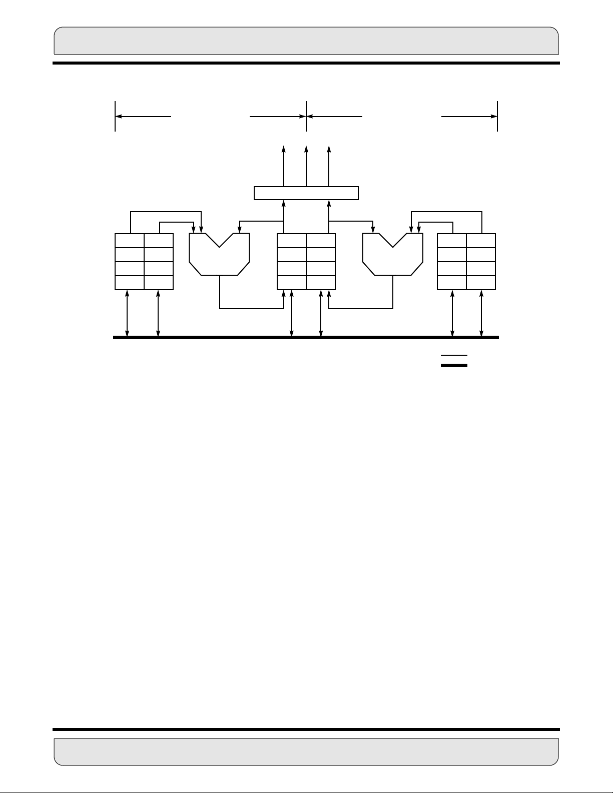
AGU ARCHITECTURE
LOW ADDRESS ALU HIGH ADDRESS ALU
XAB YAB PAB
TRIPLE MULTIPLEXER
M0
N0
N1
M1
M2
N2
N3 M3
ADDRESS
ALU
GLOBAL DATA BUS
R4
R0
R1
R5
R6
R2
R3 R7
ADDRESS
ALU
N4
M4
M5
N5
N6
M6
M7 N7
16 bits
24 bits
Figure 4-2 AGU Block Diagram
GDB. When read by the GDB, the contents of a register are placed in the two least significant bytes, and the most significant byte on the GDB is zero extended. When a register
is written, only the least significant 16 bits of the GDB are used; the upper portion is
truncated.
4.2.3 Modifier Register Files (Mn)
Each of the two modifier register files shown in Figure 4-2 consists of four 16-bit registers.
The two files contain modifier registers M0 - M3 and M4 - M7, which specify the type of
arithmetic used during address register update calculations or contain data. Each modifier
register can be read or written by the GDB. When read by the GDB, the contents of a register are placed in the two least significant bytes, and the most significant byte on the GDB
is zero extended. When a register is written, only the least significant 16 bits of the GDB
are used; the upper portion is truncated. Each modifier register is preset to $FFFF during
a processor reset.
4.2.4 Address ALU
The two address ALUs are identical (see Figure 4-2) in that each contains a 16-bit full
adder (called an offset adder), which can add 1) plus one, 2) minus one, 3) the contents
of the respective offset register N, or 4) the twos complement of N to the contents of the
MOTOROLA ADDRESS GENERATION UNIT 4 - 5
Page 59

selected address register. A second full adder (called a modulo adder) adds the summed
result of the first full adder to a modulo value, M or minus M, where M-1 is stored in the
respective modifier register. A third full adder (called a reverse-carry adder) can add 1)
plus one, 2) minus one, 3) the offset N (stored in the respective offset register), or 4) minus
N to the selected address register with the carry propagating in the reverse direction —
i.e., from the most significant bit (MSB) to the least significant bit (LSB). The offset adder
and the reverse-carry adder are in parallel and share common inputs. The only difference
between them is that the carry propagates in opposite directions. Test logic determines
which of the three summed results of the full adders is output.
Each address ALU can update one address register, Rn, from its respective address register file during one instruction cycle and can perform linear, reverse-carry, and modulo
arithmetic. The contents of the selected modifier register specify the type of arithmetic to
be used in an address register update calculation. The modifier value is decoded in the
address ALU.
PROGRAMMING MODEL
The output of the offset adder gives the result of linear arithmetic (e.g., Rn
and is selected as the modulo arithmetic unit output for linear arithmetic addressing modifiers. The reverse-carry adder performs the required operation for reverse-carry
arithmetic and its result is selected as the address ALU output for reverse-carry addressing modifiers. Reverse-carry arithmetic is useful for 2
addressing. For modulo arithmetic, the modulo arithmetic unit will perform the function
(Rn
Nn. If the modulo operation requires wraparound for modulo arithmetic, the summed output of the modulo adder gives the correct updated address register value; if wraparound
is not necessary, the output of the offset adder gives the correct result.
4.2.5 Address Output Multiplexers
The address output multiplexers (see Figure 4-2) select the source for the XAB, YAB, and
PAB. These multiplexers allow the XAB, YAB, or PAB outputs to originate from R0 - R3
or R4 - R7.
4.3 PROGRAMMING MODEL
The programmer’s view of the AGU is eight sets of three registers (see Figure 4-3). These
registers can act as temporary data registers and indirect memory pointers. Automatic updating is available when using address register indirect addressing. The Mn registers can
be programmed for linear addressing, modulo addressing, and bit-reverse addressing.
N) modulo M, where N can be one, minus one, or the contents of the offset register
±
k
-point fast Fourier transform (FFT)
±
1; Rn
±
N)
4 - 6 ADDRESS GENERATION UNIT
MOTOROLA
Page 60

PROGRAMMING MODEL
23 16 15 0
*
*
*
*
*
*
*
*
ADDRESS REGISTERS
* Written as don’t care; read as zero
R7
R6
R5
R4
R3
R2
R1
R0
23 16 15 0
*
*
*
*
*
*
*
*
OFFSET REGISTERS
N7
N6
N5
N4
N3
N2
N1
N0
23 16 15 0
*
*
*
*
*
*
*
*
MODIFIER REGISTERS
M7
M6
M5
M4
M3
M2
M1
M0
UPPER FILE
LOWER FILE
Figure 4-3 AGU Programming Model
4.3.1 Address Register Files (R0 - R3 and R4 - R7)
The eight 16-bit address registers, R0 - R7, can contain addresses or general-purpose
data. The 16-bit address in a selected address register is used in the calculation of the
effective address of an operand. When supporting parallel X and Y data memory moves,
the address registers must be thought of as two separate files, R0 - R3 and R4 - R7. The
contents of an Rn may point directly to data or may be offset. In addition, Rn can be preupdated or post-updated according to the addressing mode selected. If an Rn is updated,
modifier registers, Mn, are always used to specify the type of update arithmetic. Offset
registers, Nn, are used for the update-by-offset addressing modes. The address register
modification is performed by one of the two modulo arithmetic units. Most addressing
modes modify the selected address register in a read-modify-write fashion; the address
register is read, its contents are modified by the associated modulo arithmetic unit, and
the register is written with the appropriate output of the modulo arithmetic unit. The form
of address register modification performed by the modulo arithmetic unit is controlled by
the contents of the offset and modifier registers discussed in the following paragraphs. Address registers are not affected by a processor reset.
4.3.2 Offset Register Files (N0
-
N3 and N4
-
N7)
The eight 16-bit offset registers, N0 - N7, can contain offset values used to increment/decrement address registers in address register update calculations or can be used for 16-bit
general-purpose storage. For example, the contents of an offset register can be used to
step through a table at some rate (e.g., five locations per step for waveform generation),
or the contents can specify the offset into a table or the base of the table for indexed addressing. Each address register, Rn, has its own offset register, Nn, associated with it.
MOTOROLA ADDRESS GENERATION UNIT 4 - 7
Page 61

ADDRESSING
Table 4-1 Address Register Indirect Summary
Address Register Indirect
No Update No XXXX X (Rn)
Postincrement by 1 Yes XXXX X (Rn)+
Postdecrement by 1 Yes XXXX X (Rn)–
Postincrement by Offset Nn Yes XXXX X (Rn)+Nn
NOTE:
S = System Stack Reference
C = Program Control Unit Register Reference
D = Data ALU Register Reference
A = Address ALU Register Reference
P = Program Memory Reference
X = X Memory Reference
Y = Y Memory Reference
L = L Memory Reference
XY = XY Memory Reference
Uses Mn
Modifier
SCDAPXYLXY
Operand Reference
Assembler
Syntax
Offset registers are not affected by a processor reset.
4.3.3 Modifier Register Files (M0
-
M3 and M4 - M7)
The eight 16-bit modifier registers, M0 - M7, define the type of address arithmetic to be
performed for addressing mode calculations, or they can be used for general-purpose
storage. The address ALU supports linear, modulo, and reverse-carry arithmetic types for
all address register indirect addressing modes. For modulo arithmetic, the contents of Mn
also specify the modulus. Each address register, Rn, has its own modifier register, Mn,
associated with it. Each modifier register is set to $FFFF on processor reset, which specifies linear arithmetic as the default type for address register update calculations.
4.4 ADDRESSING
The DSP56K provides three different addressing modes: register direct, address register
indirect, and special. Since the register direct and special addressing modes do not necessarily use the AGU registers, they are described in SECTION 6 - INSTRUCTION SET
INTRODUCTION. The address register indirect addressing modes use the registers in
4 - 8 ADDRESS GENERATION UNIT
MOTOROLA
Page 62

ADDRESSING
the AGU and are described in the following paragraphs.
4.4.1 Address Register Indirect Modes
When an address register is used to point to a memory location, the addressing mode is
called “address register indirect” (see Table 4-1). The term indirect is used because the
register contents are not the operand itself, but rather the address of the operand. These
addressing modes specify that an operand is in memory and specify the effective
address of that operand.
A portion of the data bus movement field in the instruction specifies the memory space to
be referenced. The contents of specific AGU registers that determine the effective
address are modified by arithmetic operations performed in the AGU. The type of
address arithmetic used is specified by the address modifier register, Mn. The offset register, Nn, is only used when the update specifies an offset.
Not all possible combinations are available, such as + (Rn). The 24-bit instruction word
size is not large enough to allow a completely orthogonal instruction set for all instructions used by the DSP.
An example and description of each mode is given in the following paragraphs. SECTION 6 - INSTRUCTION SET INTRODUCTION and APPENDIX A - INSTRUCTION SET
DETAILS give a complete description of the instruction syntax used in these examples.
In particular, XY: memory references refer to instructions in which an operand in X memory and an operand in Y memory are referenced in the same instruction.
4.4.1.1 No Update
The address of the operand is in the address register, Rn (see Table 4-1). The contents
of the Rn register are unchanged by executing the instruction. Figure 4-4 shows a MOVE
instruction using address register indirect addressing with no update. This mode can be
used for making XY: memory references. This mode does not use Nn or Mn registers.
4.4.1.2 Postincrement By 1
The address of the operand is in the address register, Rn (see Table 4-1 and Figure 4-5).
After the operand address is used, it is incremented by 1 and stored in the same address
register. This mode can be used for making XY: memory references and for modifying
the contents of Rn without an associated data move.
4.4.1.3 Postdecrement By 1
The address of the operand is in the address register, Rn (see Table 4-1 and Figure 4-6).
After the operand address is used, it is decremented by 1 and stored in the same
address register. This mode can be used for making XY: memory references and for
MOTOROLA ADDRESS GENERATION UNIT 4 - 9
Page 63

EXAMPLE: MOVE A1,X: (R0)
ADDRESSING
BEFORE EXECUTION
A2 A1 A0
55 48 47 24 23 0
0123456789ABCD
7 0 23 0 23 0
X MEMORY
23 0
XXXXXX
$1000 $1000
15 0
$1000
R0
15 0
N0
M0
XXXX
15 0
$FFFF
AFTER EXECUTION
A2 A1 A0
55 48 47 24 23 0
0 123456789ABCD
7 0 23 0 23 0
X MEMORY
23 0
$234567
15 0
R0
N0
M0
$1000
15 0
XXXX
15 0
$FFFF
Assembler Syntax: (Rn)
Memory Spaces: P:, X:, Y:, XY:, L:
Additional Instruction Execution Time (Clocks): 0
Additional Effective Address Words: 0
Figure 4-4 Address Register Indirect — No Update
modifying the contents of Rn without an associated data move.
4.4.1.4 Postincrement By Offset Nn
The address of the operand is in the address register, Rn (see Table 4-1 and Figure 4-7).
After the operand address is used, it is incremented by the contents of the Nn register and
stored in the same address register. The contents of the Nn register are unchanged. This
mode can be used for making XY: memory references and for modifying the contents of
4 - 10 ADDRESS GENERATION UNIT
MOTOROLA
Page 64

EXAMPLE: MOVE B0,Y: (R1)+
BEFORE EXECUTION AFTER EXECUTION
ADDRESSING
B2 B1 B0
55 48 47 24 23 0
AF654321FEDCBA
7 0 23 0 23 0
Y MEMORY
23 0
$2501
$2500
XXXXXX
XXXXXX
15 0
R1
N1
M1
$2500
15 0
XXXX
15 0
$FFFF
B2 B1 B0
55 48 47 24 23 0
AF654321FEDCBA
7 0 23 0 23 0
Y MEMORY
23 0
$2501
$2500
XXXXXXX
$FEDCBA
15 0
R1
N1
M1
$2501
15 0
XXXX
15 0
$FFFF
Assembler Syntax: (Rn)+
Memory Spaces: P:, X:, Y:, XY:, L:
Additional Instruction Execution Time (Clocks): 0
Additional Effective Address Words: 0
Figure 4-5 Address Register Indirect — Postincrement
Rn without an associated data move.
4.4.1.5 Postdecrement By Offset Nn
The address of the operand is in the address register, Rn (see Table 4-1 and Figure 4-8).
After the operand address is used, it is decremented by the contents of the Nn register
and stored in the same address register. The contents of the Nn register are unchanged.
This mode cannot be used for making XY: memory references, but it can be used to mod-
MOTOROLA ADDRESS GENERATION UNIT 4 - 11
Page 65

EXAMPLE: MOVE Y0,Y: (R3)-
ADDRESSING
BEFORE EXECUTION
Y1 Y0
47 24 23 0
1231 23 4564 56
23 0 23 0
Y MEMORY
23 0
$4735
$4734
XXXXXX
XXXXXX
15 0
R3
N3
M3
$4735
15 0
XXXX
15 0
$FFFF
AFTER EXECUTION
47 24 23 0
23 0 23 0
Y1 Y0
12 31 23 4 564 56
Y MEMORY
23 0
$4735
$4734
456456
XXXXXX
15 0
R3
N3
M3
$4734
15 0
XXXX
15 0
$FFFF
Assembler Syntax: (Rn)–
Memory Spaces: P:, X:, Y:, XY:, L:
Additional Instruction Execution Time (Clocks): 0
Additional Effective Address Words: 0
Figure 4-6 Address Register Indirect — Postdecrement
ify the contents of Rn without an associated data move.
4.4.1.6 Indexed By Offset Nn
The address of the operand is the sum of the contents of the address register, Rn, and
the contents of the address offset register, Nn (see Table 4-1 and Figure 4-9). The contents of the Rn and Nn registers are unchanged. This addressing mode, which requires
4 - 12 ADDRESS GENERATION UNIT
MOTOROLA
Page 66

EXAMPLE: MOVE X1,X: (R2)+N2
ADDRESSING
BEFORE EXECUTION
47 24 23 0
23 0 23 0
X1 X0
A5 B4C6 000001
X MEMORY
23 0
$3204
$3200
XXXXXX
XXXXXX
15 0
R2
N2
M2
$3200
15 0
$0004 $0004
15 0
$FFFF
AFTER EXECUTION
X1 X0
47 24 23 0
A5B4C6 000001
23 0 23 0
X MEMORY
23 0
$3204
$3200
XXXXXX
$A5B4 C6
15 0
R2
N2
M2
$3204
15 0
15 0
$FFFF
Assembler Syntax: (Rn)+Nn
Memory Spaces: P:, X:, Y:, XY:, L:
Additional Instruction Execution Time (Clocks): 0
Additional Effective Address Words: 0
Figure 4-7 Address Register Indirect — Postincrement by Offset Nn
an extra instruction cycle, cannot be used for making XY: memory references.
4.4.1.7 Predecrement By 1
The address of the operand is the contents of the address register, Rn, decremented by
1 before the operand address is used (see Table 4-1 and Figure 4-10). The contents of
Rn are decremented and stored in the same address register. This addressing mode requires an extra instruction cycle. This mode cannot be used for making XY: memory
references, nor can it be used for modifying the contents of Rn without an associated data
MOTOROLA ADDRESS GENERATION UNIT 4 - 13
Page 67

EXAMPLE: MOVE X:(R4)–N4,A0
ADDRESSING
BEFORE EXECUTION
A2 A1 A0
55 48 47 24 23 0
0 F74105A 3FA6B0
7 0 23 0 23 0
X MEMORY
23 0
$7706
$7703
$505050
XXXXXX
15 0
R4
N4
M4
$7706
15 0
$0003
15 0
$FFFF
AFTER EXECUTION
A2 A1 A0
55 48 47 24 23 0
0F74105A505050
7 0 23 0 23 0
X MEMORY
23 0
$7706
$7703
$505050
XXXXXX
15 0
$7703
R4
15 0
$0003
N4
15 0
M4
$FFFF
Assembler Syntax: (Rn)–Nn
Memory Spaces: P:, X:, Y:, L:
Additional Instruction Execution Time (Clocks): 0
Additional Effective Address Words: 0
Figure 4-8 Address Register Indirect — Postdecrement by Offset Nn
move.
4.4.2 Address Modifier Arithmetic Types
The address ALU supports linear, modulo, and reverse-carry arithmetic for all address
register indirect modes. These arithmetic types easily allow the creation of data structures
in memory for FIFOs (queues), delay lines, circular buffers, stacks, and bit-reversed FFT
buffers.
4 - 14 ADDRESS GENERATION UNIT
MOTOROLA
Page 68

EXAMPLE: MOVE Y1,X: (R6+N6)
ADDRESSING
BEFORE EXECUTION
Y1 Y0
47 24 23 0
62100 9BA4C22
23 0 23 0
X MEMORY
23 0
$6004
$6000
XXXXXX
XXXXXX
15 0
R6
N6
M6
$6000
15 0
$0004 $0004
15 0
$FFFF
AFTER EXECUTION
Y1 Y0
47 24 23 0
62100 9B A4 C22
23 0 23 0
X MEMORY
23 0
$6004
$6000
+
$621009
XXXXXX
15 0
R6
N6
M6
$6000
15 0
15 0
$FFFF
Assembler Syntax: (Rn+Nn)
Memory Spaces: P:, X:, Y:, L:
Additional Instruction Execution Time (Clocks): 2
Additional Effective Address Words: 0
Figure 4-9 Address Register Indirect — Indexed by Offset Nn
The contents of the address modifier register, Mn, defines the type of arithmetic to be performed for addressing mode calculations. For modulo arithmetic, the contents of Mn also
specifies the modulus, or the size of the memory buffer whose addresses will be referenced. See Table 4-2 for a summary of the address modifiers implemented on the
MOTOROLA ADDRESS GENERATION UNIT 4 - 15
Page 69

EXAMPLE: MOVE X: –(R5),B1
ADDRESSING
BEFORE EXECUTION
B2 B1 B0
55 48 47 24 23 0
3BB62D04A554C0
7 0 23 0 23 0
X MEMORY
23 0
$3007
$3006
$ABCDEF
$123456
15 0
R5
N5
M5
$3007
15 0
XXXX
15 0
$FFFF
AFTER EXECUTION
B2 B1 B0
55 48 47 24 23 0
3B12345 6A554C 0
7 0 23 0 23 0
X MEMORY
23 0
$3007
$3006
$ABCDEF
$123456
15 0
R5
N5
M5
$3006
15 0
XXXX
15 0
$FFFF
Assembler Syntax: –Rn
Memory Spaces: P:, X:, Y:, L:
Additional Instruction Execution Time (Clocks): 2
Additional Effective Address Words: 0
Figure 4-10 Address Register Indirect — Predecrement
DSP56K. The MMMM column indicates the hex value which should be stored in the Mn
register.
4.4.2.1 Linear Modifier (Mn=$FFFF)
When the value in the modifier register is $FFFF, address modification is performed using
normal 16-bit linear arithmetic (see Table 4-2). A 16-bit offset, Nn, and + 1 or –1 can be
used in the address calculations. The range of values can be considered as signed (Nn
from –32,768 to + 32,767) or unsigned (Nn from 0 to + 65,535) since there is no arithmetic
4 - 16 ADDRESS GENERATION UNIT
MOTOROLA
Page 70

ADDRESSING
difference between these two data representations. Addresses are normally considered
unsigned, and data is normally considered signed.
4.4.2.2 Modulo Modifier
When the value in the modifier register falls into one of two ranges (Mn=$0001 to $7FFF
or Mn= $8001 to $BFFF with the reserved gaps noted in the table), address modification
is performed using modulo arithmetic (see Table 4-2).
Modulo arithmetic normally causes the address register value to remain within an address
range of size M, whose lower boundary is determined by Rn. The upper boundary is determined by the modulus, or M. The modulus value, in turn, is determined by Mn, the value
in the modifier register (see Figure 4-11).
There are certain cases where modulo arithmetic addressing conditions may cause the
address register to jump linearly to the same relative address in a different buffer. Other
cases firmly restrict the address register to the same buffer, causing the address register
to wrap around within the buffer. The range in which the value contained in the modifier
register falls determines how the processor will handle modulo addressing.
4.4.2.2.1 Mn=$0001 to $7FFF
In this range, the modulus (M) equals the value in the modifier register (Mn) plus 1. The
memory buffer’s lower boundary (base address) value, determined by Rn, must have zeros in the k LSBs, where 2
k
≥
M, and therefore must be a multiple of 2
k
. The upper
boundary is the lower boundary plus the modulo size minus one (base address plus M–
1). Since M
k
2
) is created where these circular buffers can be located. If M<2k, there will be a space
between sequential circular buffers of (2
2k, once M is chosen, a sequential series of memory blocks (each of length
≤
k
)–M.
For example, to create a circular buffer of 21 stages, M is 21, and the lower address
boundary must have its five LSBs equal to zero (2
k
≥ 21, thus k ≥ 5). The Mn register is
loaded with the value 20. The lower boundary may be chosen as 0, 32, 64, 96, 128, 160,
etc. The upper boundary of the buffer is then the lower boundary plus 21. There will be an
unused space of 11 memory locations between the upper address and next usable lower
address. The address pointer is not required to start at the lower address boundary or to
end on the upper address boundary; it can initially point anywhere within the defined modulo address range. Neither the lower nor the upper boundary of the modulo region is
stored; only the size of the modulo region is stored in Mn. The boundaries are determined
by the contents of Rn. Assuming the (Rn)+ indirect addressing mode, if the address register pointer increments past the upper boundary of the buffer (base address plus M–1),
it will wrap around through the base address (lower boundary). Alternatively, assuming
the (Rn)- indirect addressing mode, if the address decrements past the lower boundary
MOTOROLA ADDRESS GENERATION UNIT 4 - 17
Page 71

ADDRESSING
Table 4-2 Address Modifier Summary
MMMM Addressing Mode Arithmetic
0000 Reverse Carry (Bit Reverse)
0001 Modulo 2
0002 Modulo 3
::
7FFE Modulo 32767
7FFF Modulo 32768
8000 Reserved
8001 Multiple Wrap-Around Modulo 2
8002 Reserved
8003 Multiple Wrap-Around Modulo 4
: Reserved
8007 Multiple Wrap-Around Modulo 8
: Reserved
800F Multiple Wrap-Around Modulo 2
: Reserved
801F Multiple Wrap-Around Modulo 2
: Reserved
803F Multiple Wrap-Around Modulo 2
: Reserved
807F Multiple Wrap-Around Modulo 2
: Reserved
80FF Multiple Wrap-Around Modulo 2
: Reserved
81FF
: Reserved
83FF
: Reserved
87FF Multiple Wrap-Around Modulo 2
: Reserved
8FFF
: Reserved
9FFF Multiple Wrap-Around Modulo 2
: Reserved
BFFF Multiple Wrap-Around Modulo 2
: Reserved
Multiple Wrap-Around Modulo 2
Multiple Wrap-Around Modulo 2
Multiple Wrap-Around Modulo 2
4
5
6
7
8
9
10
11
12
13
14
4 - 18 ADDRESS GENERATION UNIT MOTOROLA
Page 72

ADDRESSING
UPPER BOUNDARY
ADDRESS
POINTER
CIRCULAR
BUFFER
M = MODULUS
LOWER BOUNDARY
Figure 4-11 Circular Buffer
(base address), it will wrap around through the base address plus M–1 (upper boundary).
If an offset (Nn) is used in the address calculations, the 16-bit absolute value, |Nn|, must
be less than or equal to M for proper modulo addressing in this range. If Nn>M, the result
is data dependent and unpredictable, except for the special case where Nn=P x 2
k
, a multiple of the block size where P is a positive integer. For this special case, when using the
(Rn)+ Nn addressing mode, the pointer, Rn, will jump linearly to the same relative address
in a new buffer, which is P blocks forward in memory (see Figure 4-12).
Similarly, for (Rn)–Nn, the pointer will jump P blocks backward in memory. This technique
is useful in sequentially processing multiple tables or N-dimensional arrays. The range of
values for Nn is –32,768 to + 32,767. The modulo arithmetic unit will automatically wrap
around the address pointer by the required amount. This type of address modification is
useful for creating circular buffers for FIFOs (queues), delay lines, and sample buffers up
to 32,768 words long as well as for decimation, interpolation, and waveform generation.
The special case of (Rn)
± Nn mod M with Nn=P x 2
k
is useful for performing the same
algorithm on multiple blocks of data in memory — e.g., parallel infinite impulse response
(IIR) filtering.
An example of address register indirect modulo addressing is shown in Figure 4-13. Starting at location 64, a circular buffer of 21 stages is created. The addresses generated are
offset by 15 locations. The lower boundary = L x (2
k
) where 2k ≥ 21; therefore, k=5 and
the lower address boundary must be a multiple of 32. The lower boundary may be chosen
MOTOROLA ADDRESS GENERATION UNIT 4 - 19
Page 73

ADDRESSING
k
2
M
(Rn) ± Nn MOD M
WHERE Nn = 2
k
2
M
k
(i.e., P = 1)
Figure 4-12 Linear Addressing with a Modulo Modifier
as 0, 32, 64, 96, 128, 160, etc. For this example, L is arbitrarily chosen to be 2, making
the lower boundary 64. The upper boundary of the buffer is then 84 (the lower boundary
plus 20 (M–1)). The Mn register is loaded with the value 20 (M–1). The offset register is
arbitrarily chosen to be 15 (Nn
≤M). The address pointer is not required to start at the lower
address boundary and can begin anywhere within the defined modulo address range —
i.e., within the lower boundary + (2
k
) address region. The address pointer, Rn, is arbitrarily
chosen to be 75 in this example. When R2 is post-incremented by the offset by the MOVE
instruction, instead of pointing to 90 (as it would in the linear mode) it wraps around to 69.
If the address register pointer increments past the upper boundary of the buffer (base address plus M–1), it will wrap around to the base address. If the address decrements past
the lower boundary (base address), it will wrap around to the base address plus M–1.
If Rn is outside the valid modulo buffer range and an operation occurs that causes Rn to
be updated, the contents of Rn will be updated according to modulo arithmetic rules. For
example, a MOVE B0,X:(R0)+ N0 instruction (where R0=6, M0=5, and N0=0) would apparently leave R0 unchanged since N0=0. However, since R0 is above the upper
boundary, the AGU calculates R0+ N0–M0–1 for the new contents of R0 and sets R0=0.
4 - 20 ADDRESS GENERATION UNIT MOTOROLA
Page 74
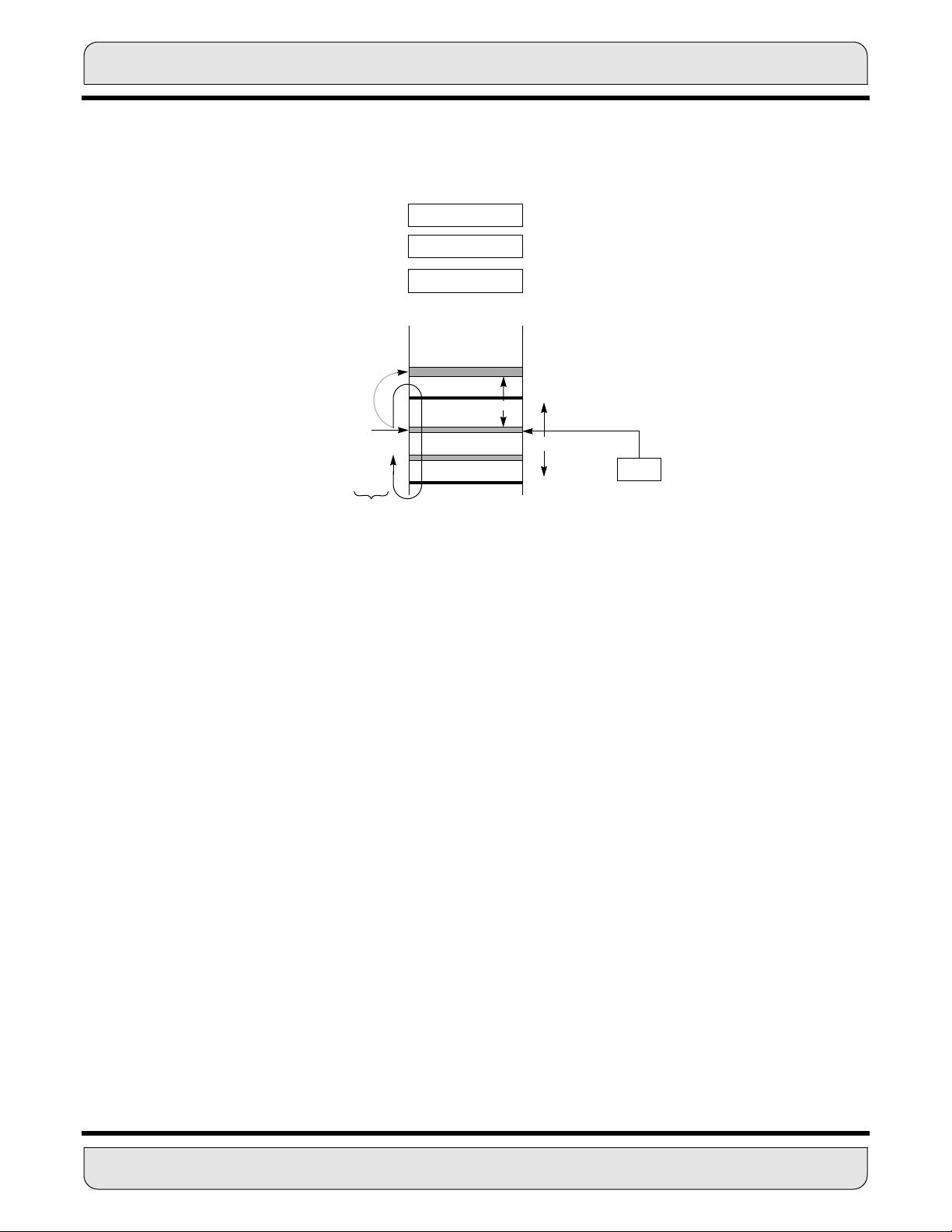
ADDRESSING
EXAMPLE: MOVE X0,X:(R2)+N
LET:
M2
00.....0010100
MODULUS=21
N2
R2
R2
0..010 00000
k=5
+
00.....0001111
00.....1001011
(90)
(75)
(69)
N2
OFFSET=15
POINTER=75
(84)
XD BUS
21
X0
(64)
Figure 4-13 Modulo Modifier Example
The MOVE instruction in Figure 4-13 takes the contents of the X0 register and moves it
to a location in the X memory pointed to by (R2), and then (R2) is updated modulo 21. The
new value of R2 is not 90 (75+ 15), which would be the case if linear arithmetic had been
used, but rather is 69 since modulo arithmetic was used.
4.4.2.2.2 Mn=$8001 to $BFFF
In this range, the modulo (M) equals (Mn+1)-$8000, where Mn is the value in the modifier register (see Table 4-2). This range firmly restricts the address register to the same
buffer, causing the address register to wrap around within the buffer. This multiple wraparound addressing feature reduces argument overhead and is useful for decimation,
interpolation, and waveform generation.
The address modification is performed modulo M, where M may be any power of 2 in the
range from 2
1
to 214. Modulo M arithmetic causes the address register value to remain
within an address range of size M defined by a lower and upper address boundary. The
value M-1 is stored in the modifier register Mn least significant 14 bits while the two most
significant bits are set to ‘10’. The lower boundary (base address) value must have zeroes
in the k LSBs, where 2
k
= M, and therefore must be a multiple of 2k. The upper boundary
is the lower boundary plus the modulo size minus one (base address plus M-1).
MOTOROLA ADDRESS GENERATION UNIT 4 - 21
Page 75

ADDRESSING
For example, to create a circular buffer of 32 stages, M is chosen as 32 and the lower address boundary must have its 5 least significant bits equal to zero (2
k
= 32, thus k = 5).
The Mn register is loaded with the value $801F. The lower boundary may be chosen as
0, 32, 64, 96, 128, 160, etc. The upper boundary of the buffer is then the lower boundary
plus 31.
The address pointer is not required to start at the lower address boundary and may begin
anywhere within the defined modulo address range (between the lower and upper boundaries). If the address register pointer increments past the upper boundary of the buffer
(base address plus M-1) it will wrap around to the base address. If the address decrements past the lower boundary (base address) it will wrap around to the base address
plus M-1. If an offset Nn is used in the address calculations, it is not required to be less
than or equal to M for proper modulo addressing since multiple wrap around is supported
for (Rn)+Nn, (Rn)-Nn and (Rn+Nn) address updates (multiple wrap-around cannot occur
with (Rn)+, (Rn)- and -(Rn) addressing modes).
The multiple wrap-around address modifier is useful for decimation, interpolation and
waveform generation since the multiple wrap-around capability may be used for argument
reduction.
4.4.2.3 Reverse-Carry Modifier (Mn=$0000)
Reverse carry is selected by setting the modifier register to zero (see Table 4-2). The address modification is performed in hardware by propagating the carry in the reverse
direction — i.e., from the MSB to the LSB. Reverse carry is equivalent to bit reversing the
contents of Rn (i.e., redefining the MSB as the LSB, the next MSB as bit 1, etc.) and the
offset value, Nn, adding normally, and then bit reversing the result. If the + Nn addressing
mode is used with this address modifier and Nn contains the value 2
(k–1)
(a power of two),
this addressing modifier is equivalent to bit reversing the k LSBs of Rn, incrementing Rn
by 1, and bit reversing the k LSBs of Rn again. This address modification is useful for addressing the twiddle factors in 2k-point FFT addressing and to unscramble 2
data. The range of values for Nn is 0 to + 32K (i.e., Nn=2
15
), which allows bit-reverse ad-
k
-point FFT
dressing for FFTs up to 65,536 points.
To make bit-reverse addressing work correctly for a 2
k
point FFT, the following proce-
dures must be used:
1. Set Mn=0; this selects reverse-carry arithmetic.
2. Set Nn=2
(k–1)
.
4 - 22 ADDRESS GENERATION UNIT MOTOROLA
Page 76
ADDRESSING
3. Set Rn between the lower boundary and upper boundary in the buffer memory. The lower boundary is L x (2
k
), where L is an arbitrary whole number. This
boundary gives a 16-bit binary number “xx . . . xx00 . . . 00”, where xx . . . xx=L
and 00 . . . 00 equals k zeros. The upper boundary is L x (2
k
)+ ((2k)–1). This
boundary gives a 16-bit binary number “xx . . . xx11 . . . 11”, where xx . . . xx=L
and 11 . . . 11 equals k ones.
4. Use the (Rn)+ Nn addressing mode.
As an example, consider a 1024-point FFT with real data stored in the X memory and
imaginary data stored in the Y memory. Since 1,024=2
is zero to select bit-reverse addressing. Offset register (Nn) contains the value 512 (2
1)
), and the pointer register (Rn) contains 3,072 (L x (2k)=3 x (210)), which is the lower
10
, k=10. The modifier register (Mn)
(k–
boundary of the memory buffer that holds the results of the FFT. The upper boundary is
4,095 (lower boundary + (2
k
)–1=3,072+ 1,023).
Postincrementing by + N generates the address sequence (0, 512, 256, 768, 128, 640,...),
which is added to the lower boundary. This sequence (0, 512, etc.) is the scrambled FFT
data order for sequential frequency points from 0 to 2
π. Table 4-3 shows the successive
contents of Rn when using (Rn)+ Nn updates.
Table 4-3 Bit-Reverse Addressing
Sequence Example
Rn Contents
3072 0
3584 512
3328 256
3840 768
3200 128
3712 640
Offset From
Lower Boundary
The reverse-carry modifier only works when the base address of the FFT data buffer is a
multiple of 2
k
, such as 1,024, 2,048, 3,072, etc. The use of addressing modes other than
postincrement by + Nn is possible but may not provide a useful result.
MOTOROLA ADDRESS GENERATION UNIT 4 - 23
Page 77

ADDRESSING
The term bit reverse with respect to reverse-carry arithmetic is descriptive. The lower
boundary that must be used for the bit-reverse address scheme to work is L x (2
k
). In the
previous example shown in Table 4-3, L=3 and k=10. The first address used is the lower
boundary (3072); the calculation of the next address is shown in Figure 4-14. The k LSBs
of the current contents of Rn (3,072) are swapped:
EACH UPDATE, (Rn)+Nn, IS EQUIVALENT TO:
L k BITS
1. BIT REVERSING: Rn=000011 0000000000=3072
0000000000
2. INCREMENT Rn BY 1: Rn=000011 0000000000
+1
000011 0000000001
3. BIT REVERSING AGAIN: Rn=000011 0000000001
1000000000
000011 1000000000=3584
Figure 4-14 Bit-Reverse Address Calculation Example
• Bits 0 and 9 are swapped.
• Bits 1 and 8 are swapped.
• Bits 2 and 7 are swapped.
• Bits 3 and 6 are swapped.
• Bits 4 and 5 are swapped.
The result is incremented (3,073), and then the k LSBs are swapped again:
• Bits 0 and 9 are swapped.
• Bits 1 and 8 are swapped.
• Bits 2 and 7 are swapped.
• Bits 3 and 6 are swapped.
• Bits 4 and 5 are swapped.
The result is Rn equals 3,584.
4 - 24 ADDRESS GENERATION UNIT MOTOROLA
Page 78

ADDRESSING
4.4.2.4 Address-Modifier-Type Encoding Summary
There are three address modifier types:
• Linear Addressing
• Reverse-Carry Addressing
• Modulo Addressing
Bit-reverse addressing is useful for 2
k
-point FFT addressing. Modulo addressing is useful
for creating circular buffers for FIFOs (queues), delay lines, and sample buffers up to
32,768 words long. The linear addressing is useful for general-purpose addressing. There
is a reserved set of modifier values (from 32,768 to 65,534) that should not be used.
Figure 4-15 gives examples of the three addressing modifiers using 8-bit registers for simplification (all AGU registers are 16 bit). The addressing mode used in the example,
postincrement by offset Nn, adds the contents of the offset register to the contents of the
address register after the address register is accessed. The results of the three examples
are as follows:
• The linear address modifier addresses every fifth location since the offset register
contains $5.
• Using the bit-reverse address modifier causes the postincrement by offset Nn
addressing mode to use the address register, bit reverse the four LSBs, increment by
1, and bit reverse the four LSBs again.
• The modulo address modifier has a lower boundary at a predetermined location, and
the modulo number plus the lower boundary establishes the upper boundary. This
boundary creates a circular buffer so that, if the address register is pointing within the
boundaries, addressing past a boundary causes a circular wraparound to the other
boundary.
MOTOROLA ADDRESS GENERATION UNIT 4 - 25
Page 79

ADDRESSING
LINEAR ADDRESS MODIFIER
M0 = 255 = 11111111 FOR LINEAR ADDRESSING WITH R0
ORIGINAL REGISTERS: N0 = 5, R0 = 75 = 0100 1011
POSTINCREMENT BY OFFSET N0: R0 = 80 = 0101 0000
POSTINCREMENT BY OFFSET N0: R0 = 85 = 0101 0101
POSTINCREMENT BY OFFSET N0: R0 = 90 = 0101 1010
MODULO ADDRESS MODIFIER
M0 = 19 = 0001 0011 FOR MODULO 20 ADDRESSING WITH R0
ORIGINAL REGISTERS: N0 = 5, R0 = 75 = 0100 1011
POSTINCREMENT BY OFFSET N0: R0 = 80 = 0101 0000
POSTINCREMENT BY OFFSET N0: R0 = 65 = 0100 0001
POSTINCREMENT BY OFFSET N0: R0 = 70 = 0100 0110
R0
R0
UPPER
BOUNDARY
LOWER
BOUNDARY
90
85
80
75
83
80
75
70
65
64
REVERSE-CARRY ADDRESS MODIFIER
M0 = 0= 0000 0000 FOR REVERSE-CARRY ADDRESSING WITH R0
ORIGINAL REGISTERS: N0 = 8, R0 = 64 = 0100 0000
POSTINCREMENT BY OFFSET N0: R0 = 72 = 0100 1000
POSTINCREMENT BY OFFSET N0: R0 = 68 = 0100 0100
POSTINCREMENT BY OFFSET N0: R0 = 76 = 0100 1100
Figure 4-15 Address Modifier Summary
R0
76
72
68
64
4 - 26 ADDRESS GENERATION UNIT MOTOROLA
Page 80

SECTION 5
PROGRAM CONTROL UNIT
MOTOROLA PROGRAM CONTROL UNIT 5 - 1
Page 81

SECTION CONTENTS
SECTION 5.1 PROGRAM CONTROL UNIT .................................................... 3
SECTION 5.2 OVERVIEW ................................................................................ 3
SECTION 5.3 PROGRAM CONTROL UNIT (PCU) ARCHITECTURE ............ 5
5.3.1 Program Decode Controller ................................................................ 5
5.3.2 Program Address Generator (PAG) ................................................... 5
5.3.3 Program Interrupt Controller ............................................................... 6
5.3.4 Instruction Pipeline Format ................................................................. 6
SECTION 5.4 PROGRAMMING MODEL ......................................................... 8
5.4.1 Program Counter ................................................................................ 8
5.4.2 Status Register ................................................................................... 9
5.4.2.1 Carry (Bit 0) .................................................................................10
5.4.2.2 Overflow (Bit 1) ...........................................................................10
5.4.2.3 Zero (Bit 2) ..................................................................................10
5.4.2.4 Negative (Bit 3) ...........................................................................10
5.4.2.5 Unnormalized (Bit 4) ...................................................................10
5.4.2.6 Extension (Bit 5) ..........................................................................11
5.4.2.7 Limit (Bit 6) ..................................................................................11
5.4.2.8 Scaling Bit (Bit 7) .........................................................................11
5.4.2.9 Interrupt Masks (Bits 8 and 9) .....................................................12
5.4.2.10 Scaling Mode (Bits 10 and 11) ..................................................12
5.4.2.11 Reserved Status (Bit 12) ...........................................................13
5.4.2.12 Trace Mode (Bit 13) ..................................................................13
5.4.2.13 Double Precision Multiply Mode (Bit 14) ...................................13
5.4.2.14 Loop Flag (Bit 15) ......................................................................13
5.4.3 Operating Mode Register ................................................................... 14
5.4.4 System Stack ...................................................................................... 14
5.4.5 Stack Pointer Register ........................................................................15
5.4.5.1 Stack Pointer (Bits 0–3) ..............................................................16
5.4.5.2 Stack Error Flag (Bit 4) ................................................................16
5.4.5.3 Underflow Flag (Bit 5) .................................................................16
5.4.5.4 Reserved Stack Pointer Registration (Bits 6–23) ........................17
5.4.6 Loop Address Register ....................................................................... 17
5.4.7 Loop Counter Register ....................................................................... 17
5.4.8 Programming Model Summary ........................................................... 17
5 - 2 PROGRAM CONTROL UNIT
MOTOROLA
Page 82

PROGRAM CONTROL UNIT
5.1 PROGRAM CONTROL UNIT
This section describes the hardware of the program control unit (PCU) and concludes
with a description of the programming model. The instruction pipeline description is also
included since understanding the pipeline is particularly important in understanding the
DSP56K family of processors.
5.2 OVERVIEW
The program control unit is one of the three execution units in the central processing
module (see Figure 5-2). It performs program address generation (instruction prefetch),
instruction decoding, hardware DO loop control, and exception (interrupt) processing.
The programmer sees the program control unit as six registers and a hardware system
stack (SS) as shown in Figure 5-1. In addition to the standard program flow-control
resources, such as a program counter (PC), complete status register (SR), and SS, the
program control unit features registers (loop address (LA) and loop counter (LC)) dedicated to supporting the hardware DO loop instruction.
The SS is a 15-level by 32-bit separate internal memory which stores the PC and SR for
subroutine calls, long interrupts, and program looping. The SS also stores the LC and LA
registers. Each location in the SS is addressable as a 16-bit register, system stack high
(SSH) and system stack low (SSL). The stack pointer (SP) points to the SS locations.
PAB PDB
16 24
CLOCK
OMR
PC
LA
LC
SP
SR
24 24
GLOBAL DATA BUS
32 x 15
STACK
INTERRUPTS
CONTROL
Figure 5-1 Program Address Generator
MOTOROLA PROGRAM CONTROL UNIT 5 - 3
Page 83

PERIPHERAL
PINS
PERIPHERAL
24-Bit
56K Mod-
MODULES
ADDRESS
GENERATION
UNIT
OVERVIEW
PROGRAM
RAM/ROM
EXPANSION
YAB
XAB
PAB
X MEMORY
RAM/ROM
EXPANSION
Y MEMORY
RAM/ROM
EXPANSION
EXPANSION
AREA
EXTERNAL
ADDRESS
BUS
SWITCH
ADDRESS
INTERNAL
DATA
BUS
SWITCH
PLL
CLOCK
GENERATOR
PROGRAM
INTERRUPT
CONTROLLER
PROGRAM
DECODE
CONTROLLER
Program Control Unit
MODC/NMI
MODB/IRQB
MODA/IRQA
RESET
PROGRAM
ADDRESS
GENERA TOR
YDB
XDB
PDB
GDB
DATA ALU
24X24+56→56-BIT MAC
TWO 56-BIT ACCUMULATORS
BUS
CONTROL
EXTERNAL
DATA BUS
SWITCH
OnCE™
16 BITS
24 BITS
PORT A
CONTROL
DATA
Figure 5-2 DSP56K Block Diagram
All of the PCU registers are read/write to facilitate system debugging. Although none of
the registers are 24 bits, they are read or written over 24-bit buses. When they are read,
the least significant bits (LSBs) are significant, and the most significant bits (MSBs) are
zeroed as appropriate. When they are written, only the appropriate LSBs are significant,
and the MSBs are written as don’t care.
5 - 4 PROGRAM CONTROL UNIT
MOTOROLA
Page 84

PROGRAM CONTROL UNIT (PCU) ARCHITECTURE
The program control unit implements a three-stage (prefetch, decode, execute) pipeline
and controls the five processing states of the DSP: normal, exception, reset, wait, and
stop.
5.3 PROGRAM CONTROL UNIT (PCU) ARCHITECTURE
The PCU consists of three hardware blocks: the program decode controller (PDC), the
program address generator (PAG), and the program interrupt controller (PIC).
5.3.1 Program Decode Controller
The PDC contains the program logic array decoders, the register address bus generator,
the loop state machine, the repeat state machine, the condition code generator, the interrupt state machine, the instruction latch, and the backup instruction latch. The PDC
decodes the 24-bit instruction loaded into the instruction latch and generates all signals
necessary for pipeline control. The backup instruction latch stores a duplicate of the
prefetched instruction to optimize execution of the repeat (REP) and jump (JMP)
instructions.
5.3.2 Program Address Generator (PAG)
The PAG contains the PC, the SP, the SS, the operating mode register (OMR), the SR,
the LC register, and the LA register (see Figure 5-1).
The PAG provides hardware dedicated to support loops, which are frequent constructs in
DSP algorithms. A DO instruction loads the LC register with the number of times the loop
should be executed, loads the LA register with the address of the last instruction word in
the loop (fetched during one loop pass), and asserts the loop flag in the SR. The DO instruction also supports nested loops by stacking the contents of the LA, LC, and SR prior
to the execution of the instruction. Under control of the PAG, the address of the first instruction in the loop is also stacked so the loop can be repeated with no overhead. While
the loop flag in the SR is asserted, the loop state machine (in the PDC) will compare the
PC contents to the contents of the LA to determine if the last instruction word in the loop
was fetched. If the last word was fetched, the LC contents are tested for one. If LC is not
equal to one, then it is decremented, and the SS is read to update the PC with the address
of the first instruction in the loop, effectively executing an automatic branch. If the LC is
equal to one, then the LC, LA, and the loop flag in the SR are restored with the stack contents, while instruction fetches continue at the incremented PC value (LA + 1). More
information about the LA and LC appears in Section 5.3.4 Instruction Pipeline Format.
The repeat (REP) instruction loads the LC with the number of times the next instruction is
to be repeated. The instruction to be repeated is only fetched once, so throughput is increased by reducing external bus contention. However, REP instructions are not
MOTOROLA PROGRAM CONTROL UNIT 5 - 5
Page 85

PROGRAM CONTROL UNIT (PCU) ARCHITECTURE
interruptible since they are fetched only once. A single-instruction DO loop can be used
in place of a REP instruction if interrupts must be allowed.
5.3.3 Program Interrupt Controller
The PIC receives all interrupt requests, arbitrates among them, and generates the interrupt vector address.
Interrupts have a flexible priority structure with levels that can range from zero to three.
Levels 0 (lowest level), 1, and 2 are maskable. Level 3 is the highest interrupt priority level
(IPL) and is not maskable. Two interrupt mask bits in the SR reflect the current IPL and
indicate the level needed for an interrupt source to interrupt the processor. Interrupts
cause the DSP to enter the exception processing state which is discussed fully in SECTION 7 – PROCESSING STATES.
The four external interrupt sources include three external interrupt request inputs (IRQA
IRQB
, and NMI) and the RESET pin. IRQA and IRQB can be either level sensitive or negative edge triggered. The nonmaskable interrupt (NMI
interrupt. MODA/IRQA
deasserted. The sampled values are stored in the operating mode register (OMR) bits
MA, MB, and MC, respectively (see Section 5.4.3 for information on the OMR). Only the
fourth external interrupt, RESET
The PIC also arbitrates between the different I/O peripherals. The currently selected peripheral supplies the correct vector address to the PIC.
5.3.4 Instruction Pipeline Format
The program control unit uses a three-level pipelined architecture in which concurrent instruction fetch, decode, and execution occur. This pipelined operation remains essentially
hidden from the user and makes programming straightforward. The pipeline is illustrated
in Figure 5-3, which shows the operations of each of the execution units and all initial conditions necessary to follow the execution of the instruction sequence shown in the figure.
The pipeline is described in more detail in Section 7.2.1 Instruction Pipeline.
The first instruction, I1, should be interpreted as follows: multiply the contents of X0 by the
contents of Y0, add the product to the contents already in accumulator A, round the result
to the “nearest even,” store the result back in accumulator A, move the contents in X data
memory (pointed to by R0) into X0 and postincrement R0, and move the contents in Y
data memory (pointed to by R4) into Y1 and postincrement R4. The second instruction,
I2, should be interpreted as follows: clear accumulator A, move the contents in X0 into the
location in X data memory pointed to by R0 and postincrement R0. Before the clear oper-
, MODB/IRQB, and MODC/NMI pins are sampled when RESET is
, and Illegal Instruction have higher priority than NMI.
) is edge sensitive and is a level 3
,
5 - 6 PROGRAM CONTROL UNIT
MOTOROLA
Page 86

PROGRAM CONTROL UNIT (PCU) ARCHITECTURE
EXAMPLE PROGRAM SEGMENT
Instruction 1 MACR X0,Y1,A X:(R0)+,X0 Y:(R4)+,Y1
Instruction 2 CLR A X0,X:(R0)+ A,Y:(R4)Instruction 3 MAC X0,Y1,A X:(R0)+,X0 Y:(R4)+,Y1
SERIAL EXECUTION OF INSTRUCTIONS
SEQUENCE OF OPERATIONS
Instruction/Data Fetch
Instruction Decode
Instruction Execution
PARALLEL PROCESSING OF INSTRUCTIONS
INSTRUCTION FETCH
INSTRUCTION DECODE
INSTRUCTION EXECUTION
PARALLEL
OPERATIONS
ADDRESS
UPDATE
(AGU)
INITIAL
CONDITIONS
R0=$0005
R4=$0008
Instruction Cycle 1
INSTRUCTION
FETCH
LOGIC
Instruction Cycle 1 Instruction Cycle 2
Instruction Cycle 2
INSTRUCTION
FETCH
1
EXECUTION OF EXAMPLE PROGRAM
I1 I2
LOGIC
INSTRUCTION
DECODE
LOGIC
Instruction Cycle 3 Instruction Cycle 5Instruction Cycle
2
1
I1
INSTRUCTION
FETCH
LOGIC
INSTRUCTION
DECODE
LOGIC
INSTRUCTION
EXECUTION
LOGIC
Instruction Cycle 3
I3
I2
I1
R0=5+1
R4=8+1
3
2
1
INSTRUCTION
INSTRUCTION
INSTRUCTION
EXECUTION
INSTRUCTION
FETCH
LOGIC
DECODE
LOGIC
LOGIC
Instruction Cycle 4 Instruction Cycle 5
I4
I3
I2
R0=6+1
R4=9–1
4
3
2
FETCH
LOGIC
INSTRUCTION
DECODE
LOGIC
INSTRUCTION
EXECUTION
LOGIC
I5
I4
I3
R0=7+1
R4=8+1
5
4
3
INSTRUCTION
EXECUTION
(DATA ALU)
X MEMORY
AT ADDRESS
$0005
$0006
$0007
Y MEMORY
AT ADDRESS
$0008
$0009
A:
A2=$00
A1=$000066
A0=$000000
X0=$400000
Y1=$000077
DATA
$000005
$000006
$000007
DATA
$000008
$000009
A:
A2=$00
A1=$0000A2
A0=$000000
X0=$000005
Y1=$000008
$000005
$000006
$000007
$000008
$000009
A:
A2=$00
A1=$000000
A0=$000000
X0=$000005
Y1=$000008
$000005
$000005
$000007
$000008
$0000A2
A:
A2=$00
A1=$000000
A0=$000050
X0=$000007
Y1=$000008
$000005
$000005
$000007
$000008
$0000A2
Figure 5-3 Three-Stage Pipeline
MOTOROLA PROGRAM CONTROL UNIT 5 - 7
Page 87

PROGRAMMING MODEL
PROGRAM CONTROL UNIT
23 1615 0
*
LOOP ADDRESS
REGISTER (LA)
23 1615 0
*
PROGRAM
COUNTER (PC)
31 SSH 1615 SSL 0
23 1615 0
*
LOOP COUNTER (LC)
23 1615 8 7 0
MR CCR
*
STATUS
REGISTER (SR)
SYSTEM STACK
Figure 5-4 Program Control Unit Programming Model
23 8 7 6 5 4 3 2 1 0
SD
MC
*
*
OPERATING MODE REGISTER (OMR)
1
23 6 5 0
*
STACK POINTER (SP)
YD
*
MADE MB
* READ AS ZERO, SHOULD BE WRITTEN
15
WITH ZERO FOR FUTURE COMPATIBILITY
ation, move the contents in accumulator A into the location in Y data memory pointed to
by R4 and postdecrement R4. The third instruction, I3, is the same as I1, except the
rounding operation is not performed.
5.4 PROGRAMMING MODEL
The program control unit features LA and LC registers which support the DO loop instruction and the standard program flow-control resources, such as a PC, complete SR, and
SS. With the exception of the PC, all registers are read/write to facilitate system debugging. Figure 5-4 shows the program control unit programming model with the six registers
and SS. The following paragraphs give a detailed description of each register.
5.4.1 Program Counter
This 16-bit register contains the address of the next location to be fetched from program
memory space. The PC can point to instructions, data operands, or addresses of operands. References to this register are always inherent and are implied by most instructions.
5 - 8 PROGRAM CONTROL UNIT
MOTOROLA
Page 88

PROGRAMMING MODEL
MR CCR
15 14 13 12 11 10 9 8 76 543210
LF DM T S1 S0 I1 I0 S L E U N Z V C
*
CARRY
OVERFLOW
ZERO
NEGATIVE
UNNORMALIZED
EXTENSION
LIMIT
SCALING
INTERRUPT MASK
SCALING MODE
RESERVED
TRACE MODE
DOUBLE PRECISION
MULTIPLY MODE
LOOP FLAG
All bits are cleared after hardware reset except bits 8 and 9 which are set to ones.
Bits 12 and 16 to 23 are reserved, read as zero and should be written with zero for future compatibility
Figure 5-5 Status Register Format
This special-purpose address register is stacked when program looping is initialized,
when a JSR is performed, or when interrupts occur (except for no-overhead fast
interrupts).
5.4.2 Status Register
The 16-bit SR consists of a mode register (MR) in the high-order eight bits and a condition
code register (CCR) in the low-order eight bits, as shown in Figure 5-5. The SR is stacked
when program looping is initialized, when a JSR is performed, or when interrupts occur,
(except for no-overhead fast interrupts).
The MR is a special purpose control register which defines the current system state of the
processor. The MR bits are affected by processor reset, exception processing, the DO,
end current DO loop (ENDDO), return from interrupt (RTI), and SWI instructions and by
instructions that directly reference the MR register, such as OR immediate to control register (ORI) and AND immediate to control register (ANDI). During processor reset, the
interrupt mask bits of the MR will be set. The scaling mode bits, loop flag, and trace bit will
be cleared.
MOTOROLA PROGRAM CONTROL UNIT 5 - 9
Page 89

PROGRAMMING MODEL
The CCR is a special purpose control register that defines the current user state of the
processor. The CCR bits are affected by data arithmetic logic unit (ALU) operations, parallel move operations, and by instructions that directly reference the CCR (ORI and
ANDI). The CCR bits are not affected by parallel move operations unless data limiting occurs when reading the A or B accumulators. During processor reset, all CCR bits are
cleared.
5.4.2.1 Carry (Bit 0)
The carry (C) bit is set if a carry is generated out of the MSB of the result in an addition.
This bit is also set if a borrow is generated in a subtraction. The carry or borrow is generated from bit 55 of the result. The carry bit is also affected by bit manipulation, rotate, and
shift instructions. Otherwise, this bit is cleared.
5.4.2.2 Overflow (Bit 1)
The overflow (V) bit is set if an arithmetic overflow occurs in the 56-bit result. This bit indicates that the result cannot be represented in the accumulator register; thus, the register
has overflowed. Otherwise, this bit is cleared.
5.4.2.3 Zero (Bit 2)
The zero (Z) bit is set if the result equals zero; otherwise, this bit is cleared.
5.4.2.4 Negative (Bit 3)
The negative (N) bit is set if the MSB (bit 55) of the result is set; otherwise, this bit is
cleared.
5.4.2.5 Unnormalized (Bit 4)
The unnormalized (U) bit is set if the two MSBs of the most significant product (MSP)
portion of the result are identical. Otherwise, this bit is cleared. The MSP portion of the A
or B accumulators, which is defined by the scaling mode and the U bit, is computed as
follows:
S1 S0 Scaling Mode U Bit Computation
0 0 No Scaling U = (Bit 47 ⊕ Bit 46)
0 1 Scale Down U = (Bit 48 ⊕ Bit 47)
1 0 Scale Up U = (Bit 46 ⊕ Bit 45)
5 - 10 PROGRAM CONTROL UNIT
MOTOROLA
Page 90

PROGRAMMING MODEL
5.4.2.6 Extension (Bit 5)
The extension (E) bit is cleared if all the bits of the integer portion of the 56-bit result are
all ones or all zeros; otherwise, this bit is set. The integer portion, defined by the scaling
mode and the E bit, is computed as follows:
S1 S0 Scaling Mode Integer Portion
0 0 No Scaling Bits 55,54........48,47
0 1 Scale Down Bits 55,54........49,48
1 0 Scale Up Bits 55,54........47,46
If the E bit is cleared, then the low-order fraction portion contains all the significant bits;
the high-order integer portion is just sign extension. In this case, the accumulator extension register can be ignored. If the E bit is set, it indicates that the accumulator extension
register is in use.
5.4.2.7 Limit (Bit 6)
The limit (L) bit is set if the overflow bit is set. The L bit is also set if the data shifter/limiter
circuits perform a limiting operation; otherwise, it is not affected. The L bit is cleared only
by a processor reset or by an instruction that specifically clears it, which allows the L bit
to be used as a latching overflow bit (i.e., a “sticky” bit). L is affected by data movement
operations that read the A or B accumulator registers.
5.4.2.8 Scaling Bit (Bit 7)
The scaling bit (S) is used to detect data growth, which is required in Block Floating Point
FFT operation. Typically, the bit is tested after each pass of a radix 2 FFT and, if it is set,
the scaling mode should be activated in the next pass. The Block Floating Point FFT algorithm is described in the Motorola application note APR4/D, “Implementation of Fast
Fourier Transforms on Motorola’s DSP56000/DSP56001 and DSP96002 Digital Signal
Processors.” This bit is computed according to the following logical equations when the
result of accumulator A or B is moved to XDB or YDB. It is a “sticky” bit, cleared only by
an instruction that specifically clears it.
MOTOROLA PROGRAM CONTROL UNIT 5 - 11
Page 91

PROGRAMMING MODEL
If S1=0 and S0=0 (no scaling)
then S = (A46 XOR A45) OR (B46 XOR B45)
If S1=0 and S0=1 (scale down)
then S = (A47 XOR A46) OR (B47 XOR B46)
If S1=1 and S0=0 (scale up)
then S = (A45 XOR A44) OR (B45 XOR B44)
If S1=1 and S0=1 (reserved)
then the S flag is undefined.
where Ai and Bi means bit i in accumulator A or B.
5.4.2.9 Interrupt Masks (Bits 8 and 9)
The interrupt mask bits, I1 and I0, reflect the current IPL of the processor and indicate
the IPL needed for an interrupt source to interrupt the processor. The current IPL of the
processor can be changed under software control. The interrupt mask bits are set during
hardware reset but not during software reset.
I1 I0 Exceptions Permitted Exceptions Masked
0 0 IPL 0,1,2,3 None
0 1 IPL 1,2,3 IPL 0
1 0 IPL 2,3 IPL 0,1
1 1 IPL 3 IPL 0,1,2
5.4.2.10 Scaling Mode (Bits 10 and 11)
The scaling mode bits, S1 and S0, specify the scaling to be performed in the data ALU
shifter/limiter, and also specify the rounding position in the data ALU multiply-accumula-
5 - 12 PROGRAM CONTROL UNIT
MOTOROLA
Page 92

PROGRAMMING MODEL
tor (MAC). The scaling modes are shown in the following table:
S1 S0
0 0 23 No Scaling
0 1 24 Scale Down (1-Bit Arithmetic Right Shift)
1 0 22 Scale Up (1-Bit Arithmetic Left Shift)
1 1 — Reserved for Future Expansion
Rounding
Bit
Scaling Mode
The scaling mode affects data read from the A or B accumulator registers out to the XDB
and YDB. Different scaling modes can occur with the same program code to allow dynamic scaling. Dynamic scaling facilitates block floating-point arithmetic. The scaling mode
also affects the MAC rounding position to maintain proper rounding when different portions of the accumulator registers are read out to the XDB and YDB. The scaling mode
bits, which are cleared at the start of a long interrupt service routine, are also cleared during a processor reset.
5.4.2.11 Reserved Status (Bit 12)
This bits is reserved for future expansion and will read as zero during DSP read operations.
5.4.2.12 Trace Mode (Bit 13)
The trace mode (T) bit specifies the tracing function of the DSP56000/56001 only . (With
other members of the DSP56K family, use the OnCE trace mode described in Section
10.5.) For the DSP56000/56001, if the T bit is set at the beginning of any instruction execution, a trace exception will be generated after the instruction execution is completed. If
the T bit is cleared, tracing is disabled and instruction execution proceeds normally. If a
long interrupt is executed during a trace exception, the SR with the trace bit set will be
stacked, and the trace bit in the SR is cleared (see SECTION 7 – PROCESSING
STATES for a complete description of a long interrupt operation). The T bit is also
cleared during processor reset.
5.4.2.13 Double Precision Multiply Mode (Bit 14)
The processor is in double precision multiply mode when this bit is set. (See Section 3.4
for detailed information on the double precision multiply mode.) When the DM bit is set,
the operations performed by the MPY and MAC instructions change so that a double
precision 48-bit by 48-bit double precision multiplication can be performed in six instruc-
MOTOROLA PROGRAM CONTROL UNIT 5 - 13
Page 93

PROGRAMMING MODEL
23 8 76543210
SD MC YD DE MB MA
*
*
*
OPERATING MODE A, B
DATA ROM ENABLE
INTERNAL Y MEMORY DISABLE
OPERATING MODE C
RESERVED
STOP DELAY
RESERVED
RESERVED
Figure 5-6 OMR Format
tions. The DSP56K software simulator accurately shows how the MPY, MAC, and other
Data ALU instructions operate while the processor is in the double precision multiply
mode.
5.4.2.14 Loop Flag (Bit 15)
The loop flag (LF) bit is set when a program loop is in progress. It detects the end of a
program loop. The LF is the only SR bit that is restored when a program loop is terminated. Stacking and restoring the LF when initiating and exiting a program loop, respectively, allow the nesting of program loops. At the start of a long interrupt service routine,
the SR (including the LF) is pushed on the SS and the SR LF is cleared. When returning
from the long interrupt with an RTI instruction, the SS is pulled and the LF is restored.
During a processor reset, the LF is cleared.
5.4.3 Operating Mode Register
The OMR is a 24-bit register (only six bits are defined) that sets the current operating
mode of the processor. Each chip in the DSP56K family of processors has its own set of
operating modes which determine the memory maps for program and data memories, and
the startup procedure that occurs when the chip leaves the reset state. The OMR bits are
only affected by processor reset and by the ANDI, ORI, and MOVEC instructions, which
directly reference the OMR.
The OMR format with all of its defined bits is shown in Figure 5-6. For product-specific
OMR bit definitions, see the individual chip’s user manual for details on its respective operating modes.
5.4.4 System Stack
The SS is a separate 15X32-bit internal memory divided into two banks, the SSH and the
5 - 14 PROGRAM CONTROL UNIT
MOTOROLA
Page 94

PROGRAMMING MODEL
SSL, each 16 bits wide. The SSH stores the PC contents, and the SSL stores the SR contents for subroutine calls, long interrupts, and program looping. The SS will also store the
LA and LC registers. The SS is in stack memory space; its address is always inherent and
implied by the current instruction.
The contents of the PC and SR are pushed on the top location of the SS when a subroutine call or long interrupt occurs. When a return from subroutine (RTS) occurs, the
contents of the top location in the SS are pulled and put in the PC; the SR is not affected.
When an RTI occurs, the contents of the top location in the SS are pulled to both the PC
and SR.
The SS is also used to implement no-overhead nested hardware DO loops. When the DO
instruction is executed, the LA:LC are pushed on the SS, then the PC:SR are pushed on
the SS. Since each SS location can be addressed as separate 16-bit registers (SSH and
SSL), software stacks can be created for unlimited nesting.
The SS can accommodate up to 15 long interrupts, seven DO loops, 15 JSRs, or combinations thereof. When the SS limit is exceeded, a nonmaskable stack error interrupt
occurs, and the PC is pushed to SS location zero, which is not implemented in hardware.
The PC will be lost, and there will be no SP from the stack interrupt routine to the program
that was executing when the error occurred.
54 3210
UF SE P3 P2 P1 P0
STACK POINTER
STACK ERROR FLAG
UNDERFLOW FLAG
Figure 5-7 Stack Pointer Register Format
5.4.5 Stack Pointer Register
The 6-bit SP register indicates the location of the top of the SS and the status of the SS
(underflow, empty, full, and overflow). The SP register is referenced implicitly by some instructions (DO, REP, JSR, RTI, etc.) or directly by the MOVEC instruction. The SP
register format is shown in Figure 5-7. The SP register works as a 6-bit counter that addresses (selects) a 15-location stack with its four LSBs. The possible SP values are
shown in Figure 5-8 and described in the following paragraphs.
5.4.5.1 Stack Pointer (Bits 0–3)
The SP points to the last location used on the SS. Immediately after hardware reset,
MOTOROLA PROGRAM CONTROL UNIT 5 - 15
Page 95

PROGRAMMING MODEL
these bits are cleared (SP=0), indicating that the SS is empty.
Data is pushed onto the SS by incrementing the SP, then writing data to the location to
which the SP points. An item is pulled off the stack by copying it from that location and
then by decrementing the SP.
5.4.5.2 Stack Error Flag (Bit 4)
The stack error flag indicates that a stack error has occurred, and the transition of the
stack error flag from zero to one causes a priority level-3 stack error exception.
When the stack is completely full, the SP reads 001111, and any operation that pushes
data onto the stack will cause a stack error exception to occur. The SR will read 010000
(or 010001 if an implied double push occurs).
Any implied pull operation with SP equal to zero will cause a stack error exception, and
the SP will read 111111 (or 111110 if an implied double pull occurs).
The stack error flag is a “sticky bit” which, once set, remains set until cleared by the user.
There is a sequence of instructions that can cause a stack overflow and, without the sticky
bit, would not be detected because the stack pointer is decremented before the stack error
interrupt is taken. The sticky bit keeps the stack error bit set until the user clears it by writing a zero to SP bit 4. It also latches the overflow/underflow bit so that it cannot be
changed by stack pointer increments or decrements as long as the stack error is set. The
overflow/underflow bit remains latched until the first move to SP is executed.
Note: When SP is zero (stack empty), instructions that read the stack without SP post-
decrement and instructions that write to the stack without SP preincrement do not cause
a stack error exception (i.e., 1) DO SSL,xxxx 2) REP SSL 3) MOVEC or move peripheral
UF SE P3 P2 P1 P0
1 1 1 1 1 0 STACK UNDERFLOW CONDITION AFTER DOUBLE PULL
1 1 1 1 1 1 STACK UNDERFLOW CONDITION
0 0 0 0 0 0 STACK EMPTY (RESET); PULL CAUSES UNDERFLOW
0 0 0 0 0 1 STACK LOCATION 1
0 0 1 1 1 0 STACK LOCATION 14
0 0 1 1 1 1 STACK LOCATION 15; PUSH CAUSES OVERFLOW
0 1 0 0 0 0 STACK OVERFLOW CONDITION
0 1 0 0 0 1 STACK OVERFLOW CONDITION AFTER DOUBLE PUSH
Figure 5-8 SP Register Values
5 - 16 PROGRAM CONTROL UNIT
MOTOROLA
Page 96

PROGRAMMING MODEL
data (MOVEP) when SSL is specified as a source or destination).
5.4.5.3 Underflow Flag (Bit 5)
The underflow flag is set when a stack underflow occurs. The underflow flag is a “sticky
bit” when the stack error flag is set. That is, when the stack error flag is set, the underflow
flag will not change state. The combination of “underflow=1” and “stack error=0” is an
illegal combination and will not occur unless it is forced by the user. If this condition is
forced by the user, the hardware will correct itself based on the result of the next stack
operation.
5.4.5.4 Reserved Stack Pointer Registration (Bits 6–23)
SP register bits 6 through 23 are reserved for future expansion and will read as zero during read operations.
5.4.6 Loop Address Register
The LA is a read/write register which is stacked into the SSH by a DO instruction and is
unstacked by end-of-loop processing or by an ENDDO instruction. The contents of the LA
register indicate the location of the last instruction word in a program loop. When that last
instruction is fetched, the processor checks the contents of the LC register (see the following section). If the contents are not one, the processor decrements the LC and takes
the next instruction from the top of the SS. If the LC is one, the PC is incremented, the
loop flag is restored (pulled from the SS), the SS is purged, the LA and LC registers are
pulled from the SS and restored, and instruction execution continues normally.
5.4.7 Loop Counter Register
The LC register is a special 16-bit counter which specifies the number of times a hardware
program loop shall be repeated. This register is stacked into the SSL by a DO instruction
and unstacked by end-of-loop processing or by execution of an ENDDO instruction. When
the end of a hardware program loop is reached, the contents of the LC register are tested
for one. If the LC is one, the program loop is terminated, and the LC register is loaded with
the previous LC contents stored on the SS. If LC is not one, it is decremented and the
program loop is repeated. The LC can be read under program control, which allows the
number of times a loop will be executed to be monitored/changed dynamically. The LC is
also used in the REP instruction
5.4.8 Programming Model Summary
The complete programming model for the DSP56K central processing module is shown
in Figure 5-9. Programming models for the peripherals are shown in the appropriate user
manuals.
MOTOROLA PROGRAM CONTROL UNIT 5 - 17
Page 97

PROGRAMMING MODEL
DATA ARITHMETIC LOGIC UNIT
47 X 0
23 0 23 0
23 1615 0
*
*
*
*
*
*
*
*
X1
23 8 7 0#23 0
23 8 7 0#23 0
R7
R6
R5
R4
R3
R2
R1
R0
POINTER
REGISTERS
X0
ACCUMULATOR REGISTERS
55 A 0
A2
55 B 0
B2
ADDRESS GENERATION UNIT
23 1615 0
*
*
*
*
*
*
*
*
OFFSET
REGISTERS
INPUT REGISTERS
47 Y 0
23 0 23 0
A1
B1
N7
N6
N5
N4
N3
N2
N1
N0
Y1
A0
23 0
B0
23 0
23 1615 0
*
*
*
*
*
*
*
*
M7
M6
M5
M4
M3
M2
M1
M0
MODIFIER
REGISTERS
Y0
UPPER FILE
LOWER FILE
PROGRAM CONTROL UNIT
23 1615 0
*
LOOP ADDRESS
REGISTER (LA)
23 1615 0
*
PROGRAM
COUNTER (PC)
31 SSH 16 15 SSL 0
23 1615 0
*
LOOP COUNTER (LC)
23 1615 8 7 0
MR CCR
*
STATUS
REGISTER (SR)
23 8 7 6 5 4 3 2 1 0
*
OPERATING MODE REGISTER (OMR)
1
23 6 5 0
*
SD
*
*
STACK POINTER (SP)
MC
YD
* READ AS ZERO, SHOULD BE WRITTEN
WITH ZERO FOR FUTURE COMPATIBILITY
# READ AS SIGN EXTENSION BITS,
WRITTEN AS DON’T CARE
15
SYSTEM STACK
Figure 5-9 DSP56K Central Processing Module Programming Model
MADE MB
5 - 18 PROGRAM CONTROL UNIT MOTOROLA
Page 98

SECTION 6
INSTRUCTION SET INTRODUCTION
Fetch F1 F2 F3 F3e F4 F5 F6 . . .
Decode D1 D2 D3 D3e D4 D5 . . .
Execute E1 E2 E3 E3e E4 . . .
Instruction
Cycle: 1 2 3 4 5 6 7 . . .
MOTOROLA INSTRUCTION SET INTRODUCTION 6 - 1
Page 99

SECTION CONTENTS
SECTION 6.1 INSTRUCTION SET INTRODUCTION ......................................3
SECTION 6.2 SYNTAX .....................................................................................3
SECTION 6.3 INSTRUCTION FORMATS ........................................................3
6.3.1 Operand Sizes ....................................................................................5
6.3.2 Data Organization in Registers ...........................................................6
6.3.2.1 Data ALU Registers ...................................................................... 6
6.3.2.2 AGU Registers .............................................................................. 7
6.3.2.3 Program Control Registers ........................................................... 8
6.3.3 Data Organization in Memory ............................................................. 9
6.3.4 Operand References ..........................................................................11
6.3.4.1 Program References ..................................................................... 11
6.3.4.2 Stack References ......................................................................... 11
6.3.4.3 Register References ..................................................................... 11
6.3.4.4 Memory References ..................................................................... 11
6.3.4.4.1 X Memory References ............................................................11
6.3.4.4.2 Y Memory References ............................................................12
6.3.4.4.3 L Memory References .............................................................12
6.3.4.4.4 YX Memory References ..........................................................12
6.3.5 Addressing Modes ..............................................................................12
6.3.5.1 Register Direct Modes .................................................................. 13
6.3.5.1.1 Data or Control Register Direct ...............................................13
6.3.5.1.2 Address Register Direct ..........................................................13
6.3.5.2 Address Register Indirect Modes .................................................. 13
6.3.5.3 Special Addressing Modes ........................................................... 14
6.3.5.3.1 Immediate Data .......................................................................14
6.3.5.3.2 Absolute Address ....................................................................14
6.3.5.3.3 Immediate Short ......................................................................14
6.3.5.3.4 Short Jump Address ...............................................................14
6.3.5.3.5 Absolute Short ........................................................................14
6.3.5.3.6 I/O Short ..................................................................................16
6.3.5.3.7 Implicit Reference ...................................................................16
6.3.5.4 Addressing Modes Summary ........................................................ 20
SECTION 6.4 INSTRUCTION GROUPS ..........................................................20
6.4.1 Arithmetic Instructions ........................................................................ 22
6.4.2 Logical Instructions .............................................................................23
6.4.3 Bit Manipulation Instructions ...............................................................24
6.4.4 Loop Instructions ................................................................................24
6.4.5 Move Instructions ................................................................................26
6.4.6 Program Control Instructions .............................................................. 27
6 - 2 INSTRUCTION SET INTRODUCTION
MOTOROLA
Page 100

INSTRUCTION SET INTRODUCTION
6.1 INSTRUCTION SET INTRODUCTION
The programming model shown in Figure 6-1 suggests that the DSP56K central processing module architecture can be viewed as three functional units which operate in
parallel: data arithmetic logic unit (data ALU), address generation unit (AGU), and program control unit (PCU). The instruction set keeps each of these units busy throughout
each instruction cycle, achieving maximal speed and maintaining minimal program size.
This section introduces the DSP56K instruction set and instruction format. The complete
range of instruction capabilities combined with the flexible addressing modes used in this
processor provide a very powerful assembly language for implementing digital signal processing (DSP) algorithms. The instruction set has been designed to allow efficient coding
for DSP high-level language compilers such as the C compiler. Execution time is minimized by the hardware looping capabilities, use of an instruction pipeline, and parallel
moves.
6.2 SYNTAX
The instruction syntax is organized into four columns: opcode, operands, and two parallelmove fields. The assembly-language source code for a typical one-word instruction is
shown in the following illustration. Because of the multiple bus structure and the parallelism of the DSP, up to three data transfers can be specified in the instruction word – one
on the X data bus (XDB), one on the Y data bus (YDB), and one within the data ALU.
These transfers are explicitly specified. A fourth data transfer is implied and occurs in the
program control unit (instruction word prefetch, program looping control, etc.). Each data
transfer involves a source and a destination.
Opcode Operands XDB YDB
MAC X0,Y0,A X:(R0)+,X0 Y:(R4)+,Y0
The opcode column indicates the data ALU, AGU, or program control unit operation to be
performed and must always be included in the source code. The operands column specifies the operands to be used by the opcode. The XDB and YDB columns specify optional
data transfers over the XDB and/or YDB and the associated addressing modes. The
address space qualifiers (X:, Y:, and L:) indicate which address space is being referenced.
Parallel moves are allowed in 30 of the 62 instructions. Additional information is presented
in APPENDIX A - INSTRUCTION SET DETAILS.
6.3 INSTRUCTION FORMATS
The DSP56K instructions consist of one or two 24-bit words – an operation word and an
optional effective address extension word. The general format of the operation word is
MOTOROLA INSTRUCTION SET INTRODUCTION 6 - 3
 Loading...