

Page 1

The Worlds Leading Cellular
Telephone Man ufact urer
Service Manual
DCS StarTac
Cellular Subsciber Group
68P09304A85
Page 2

DCS1800 StarTAC PERSONAL
CELLULAR TELEPHONE
Module Level
Repair Manual
68P09304A85-O
Page 3

DCS 1800 StarTAC CELLULAR TELEPHONE
68P09304A85-0 AGen1
19/07/97
PERFORMANCE SPECIFICATIONS -DCS 1800 StarTAC
GENERAL
TRANSMITTER
RECEIVER
SPEECH CODING
Specificat ions are subject to change without notice
CAUTION
Do not jump start vehicle or use an automotive battery charger while the vehicle adapter
option and the portable ra diotelephone are connec ted to the ve hicle el ectrical s ystem as thi s
may cause serious damage to the radio. Disconnect the radio by removi ng the cable kit fuses.
Frequency Range 1710-1785 MHz Tx
1805-1880MHz Rx
Channel Spacing 200 kHz
Number of Chann els 375 carriers w ith 8 channels per carr ier
Modulation GMSK at BT = 0.3
Transmitter Ph a se Accu rac y 5 Degrees RMS, 20 Degre es peak
Duplex Spaci ng 95MHz
Frequency Stability +/- 0.1 ppm of the downlink frequency (Rx)
Voltage Operation +3V to +5.1V dc (Battery) and +4.4V to +6.5V (External connector
Transmit Current <260 mA at 1 Watt
Stand-by Cu rrent 15mA nominal
Dimensions 98.3 mm (L) x 57.3 mm(W) x 23 mm(D)
Size (Volume) 100 cubic cm
Weight Approximately 98.5g; w it h Light Lithium I on 350mAh battery a nd antenna
Temperature Range -20°C to +55°×C
RF Power Output 30 dBm nomina l
Output Impedance 50 ohms (nominal)
Spurious Emi ssions -36 dBm up to 1 GHz, (<-30 dBm > 1 GHz)
Rx Bit Error Rate (100kbit s) <2% @ -100 dBm
Channel Hop Time 500 microseco nds
Time to Camp Approximately 10 seconds
Speech Coding Type Regular Pul se Excita tion / Lin ear Predi ctive Codi ng with Lo ng Term Pred ictio n. (RPE
LPC with LTP.
Bit Rate 13.0 kbps
Frame Duration 20 ms
Block Length 260 bits
Classes Class 1 bits = 182 bits. Class 2 bits = 78 bits
Bit Rate with FEC Encoding
22.8 kbps
COMPUTER SOFTWARE COPYRIGHTS
The Motorola products described in this instru ction manual may include copyr ighted Mot or ola computer programs stor ed in semiconducto r memories
or other media. Laws in the United States and other countries preserve for Motorola certain exclusive rights for copyrighted computer programs,
including the exclusive right to copy or reproduce in any form the copyrighted computer program. Accordingly, any copyrighted Motorola computer
programs contained in t he Motorola products desc ribed in this instruction manual may not be copied or reproduced i n any manner without the express
written permission of Motorola. Furthermore, the purchase of Motorola products shall not be deemed to grant either directly or by implicat ion, estopp el ,
or otherwise, any license und er the copyrights, patents or patent applications of Mot or ola, except for the normal non-excl us ive, royalty free license to
use that arises by operation of law in the sale of a product.
© Motorola Lt d. 1997
All Rights Reserve d
Printed in U.K.
Page 4

Customer Services Publishing
Easter Inch, Bathgate, West Lothian,
EH48 2EH, United Kingdom
AGen1
© Motorola Ltd. 1997
All Rights Reserved
Printed in U.K.
DCS 1800 StarTAC PERSONAL
CELLULAR TELEPHONE
CONTENTS LIST
19/07/97
Cellular Subscriber Group
SECTION 1 - GENERAL PAGE NUMBER
FOREWORD ix
MOTOROLA SERVICE POLICY ix
GENERAL SAFETY INFORMATION x
SECTION 2 - DESCRIPTION
SYSTEM DESCRIPTION 1
DCS SYSTEM OVERVIEW 1
TELEPHONE DESCRIPTION 5
FEATURE LIST 7
SECTION 3 - LABELLING & SIM CARDS
TRANSCEIVER LABELLING 9
INTRODUCTION 9
TITLE EXPLANATIONS 9
SIM CARD S 11
INTRODUCTION 11
SIM CARD INSERTION/REMOVAL 11
SECURITY INFORMATION 11
SECTION 4 - MANUAL - TEST MODE & VERIFICATION
MANUAL-TEST MODE 13
INTRODUCTION 13
TEST SIM INSERTION/REMOVAL 13
ACCESSING THE MANUAL-TEST MODE 13
VERIFICATION 15
INTRODUCTION 15
EQUIPMENT CONFIGURATION 15
TESTING PROCEDURE 16
iii
Page 5

DCS 1800 StarTAC CELLULAR TELEPHONE
68P09304A85-0 AGen1
19/07/97
SECTION 5 - TROUBLESHOOTING
TROUBLESHOOTING 17
INTRODUCTION 17
TROUBLESHOOTING AND REPAIR 17
TESTING AFTER REPAIR 17
PIN OUT CONNECTIONS 18
TROUBLESHOOTING AND REPAIR CHART 19/21
SECTION 6 - PERSONALITY TRANSFER
PERSONALITY TRANSFER 23
INTRODUCTION 23
NORMAL TRANSFER 23
MASTER TRANSFER 24
MASTER SIM CARD CREATION 24
SECTION 7 - DISASSEMBLY
DISASSEMBLY INSTRUCTIONS 25
INTRODUCTION 25
RECOMMENDED TOOLS 25
DISASSEMBLY PROCEDURE 25
ASSEMBLY PROCEDURE 25
STEP BY STEP DISASSEMBLY 26/35
EXPLODED DIAGRAM AND PART NUMBERS 36/37
SECTION 8 - ACCESSORIES
RECHARGEABLE BATTERY PACKS 39
INTRODUCTION 39
RECHARGING 40
EXPERT PERFORMANCE BATTERIES AND CHARGERS 40
BUILT IN E.P BATTERY FAST CHARGER 40
iv
Page 6

CONTENTS
AGen1 68P09304A85-O
19/07/97
SECTION 8 - ACCESSORIES (cont) PAGE NUMBER
NI-MH BATTERY PACKS 41
LITHIUM ION BATTERY PACKS 43
AUXILIARY BATTERY PACK 45
RAPID E.P BATTERY CHARGER 47
RAPID BATTERY CHARGER TRANSFORMER 49
CIGARETTE LIGHTER ADAPTOR/CHARGER 51
CAR KITS 53
INTRODUCTION 53
INSTALLATION INTRODUCTION 54
CAR KIT CONNECTION DIAGRAM 55
INSTALLATION PLANNING 56
COMPONENT LOCATION 56
ELECTRICAL SYSTEM POLARITY 56
USING FUSE LOOPS 56
MINIMIZING ELECTRICAL NOISE 56
CONVENIENCE ON/OFF FEATURE 56
CABLE ROUTING 57
POSSIBLE INTERFERENCE WITH ABS SYSTEMS 57
INSTALLATION 57
MOUNTING THE SMART HANDSET CRADLE 57
DHFA (ADAPTER BOX) 57
StarTAC CRADLE 58
ELECTRICAL CONNECTIONS 58
ENTERTAINMENT MUTE/AUX ALERT 59
MICROPHONE INSTALLATION 59
EXTERNAL SPEAKER INSTALLATION 59
EXTERNAL ANTENNA INSTALLATION 59
PERFORMANCE CHECKS 60
CHECKING ANTENNA PERFORMANCE 60
CHECKING ANTI SKID BRAKING SYSTEMS 61
SECTION 9 - FEED BACK FORM
FEED BACK FORM
v
Page 7

DCS 1800 StarTAC CELLULAR TELEPHONE
68P09304A85-0 AGen1
19/07/97
TYPICAL MODEL COMPLEMENT FOR DCS 1800 StarTAC
Motorola DCS StarTAC S5993ABB
Motorola/One2One DCS StarTAC S5990ABB
Motorola/E-Plus DCS StarTAC S6220ABF
Motorola/Orange DCS StarTAC S5991ABB
Motorola/Bougues DCS StarTAC S5992ABE
Note: In addition to the above, VIP versions are availa ble for the Motorola/E-Pl us and the Motorola kits. Both feature the
addition of a Desktop Cha rger (SPN4325) and an auxiliary Battery (SNN4598).
Model Description
Quantity
Supplied
SUG1120A
SUG1120A
Transceiver
One2One Transceiver
1
1
SNN4667 Standard Battery
1
SPN4278+SYN4656 Travel Charger + UK plug
1
SYN5378 Belt holster
User manual in local language
1
1
Model Description
Quantity
Supplied
SUG1043A Transceiver
1
SNN4667 Standard Battery
1
SPN4278+SYN4655 Travel Charger + Euro plug
1
SYN5378 Belt holster
User manual in local language
1
1
Model Description
Quantity
Supplied
SUG1043A Orange Transceiver
1
SNN4667 Standard Battery
1
SPN4278+SYN4656 Travel Charger + UK plug
1
SYN5378 Belt holster
User manual in local language
1
1
Model Description
Quantity
Supplied
SWF2210A Transceiver
1
SNN4667
SNN4598
Standard Battery
Auxiliary Battery
1
1
SPN4278+SYN4656 Travel Charger + UK plug
1
SYN5378 Belt holster
User manual in local language
1
1
viii
Page 8

DCS 1800 StarTAC CELLULAR TELEPHONE
68P09304A85-0 AGen1
19/07/97
1. SCOPE OF MANUAL
This manual is intende d for use by experie nced technic ians fami liar with si milar ty pes of eq uipment. It contains all servi ce information
required for the equipment described and is current as of the printing date. Major changes which occur after the printing date are
incorporated by C ellula r Ma nual Re visi ons (CMR ). The se CMR ’s are ad ded to t he manuals as t he engi ne ering c hang e is incorpor at ed
into the equipment.
2. MODEL AND KIT IDENTIFICATION
Motor ola equ ipm ents are spec ifica lly ide ntif ied by an ove rall m odel n umbe r on t he na meplat e. In most ca ses, as sem blies a nd ki ts
which make up the equipment also have kit model numbers stamped on t hem. When a produ ction or engi neering change is incorporat ed,
the applicable schematic diagrams are updated.
MOTOROLA SERVICE POLICY (DCS 1800) StarTAC
Warranty:
Product will be sol d with the standard 12 months warranty terms and conditions.
Accidental damage, misus e, and re ta ilers ex tended warranti es wi ll not be s upporte d under wa rranty. Non warran ty repa irs
will be available at agreed fixed repair prices. Proof of purchase will be required to validate warranty claims.
Core Product
:
Motorola only branded product will be supported under a Low tier DCS Loaner program or alternative low cost service
strategy (To be agreed with the Eur opean Cust omer Servi ce Mana gers) . The cust omers ori ginal te le phone wil l be repa ired
but not refurbish ed as s tandard.
Appointed Motorol a Service hubs may p erform both Warranty and Non Warranty field service for Level 2 (m odule repair)
and 3 (Limited compone nt). The Motorola HTC’s will perform f ull Level 4 (full pcb component lev el) repairs.
Customer support (End User)
:
This will be available through the operator own dedicated Call Centres and In Country Help Desks. Operators will be
supported as required by the local Motorola Country Service Manager.
Product Service training should be arrange d through the local Motorola National Support Centre.
REPLACEMENT PARTS ORDERING
Only centres authorized by Motorola to carry out repairs will be able to purchase spare parts. Orders for spare parts from
HUB’s, Motorola National Support Centres and Hi-Tech Centres, should be placed with the appropriate Motorola Parts
Distributi on Centre.
BOARD REPAIRS
All centres au thorize d to ca rry out module lev el r epairs, must return fa ulty boa rds to t he appropr ia te HUB or Motorola HiTech Centre for repair to component level.
FOREWORD
ORDERING INFORMATION
ix
Page 9

CONTENTS
AGen1 68P09304A85-O
19/07/97
GENERAL SAFETY INFORMATION
PORTABLE OPERATION:
DO NOT hold the radio so that the aerial is very close to, or t ouching, exposed parts of the body, especially the
face or eyes whilst transmitting. The radio wi ll perform best if it is held in the same manner as you would hold
a ‘land’ telephone handset, with the aerial angled up and over your shoulder.
DO NOT operate the portable phone in an aircraft. Switch off your telephone. The use of a cellular telephone
in an aircraft may be dangerous to the operation of the aircraft, disrupt the Cellular Network, and is illegal.
Failure to observe this instruction m ay lead to a suspension or denial of Cellular Telephone Service to the
offender, or legal action, or both.
MOBILE/PORTABLE OPERATION - Telephone use in Vehicles
:
All equipment must be properly grounded according to installation instructions for safe operation.
Users are advised to turn off their equipment when at a refuelling point.
Safety is every drivers busines s. Cellular telephones should only be used in situations in which the driver
considers it saf e to do so.
GENERAL
:
DO NOT allow children to play with any radio equipment containing a transmitter.
DO NOT operate this equipment near electrical blasting caps or in an explosive atmosphere. Mobile telephones
are, under certain conditions, capable of interfering with blasting operations. When you are in the vicinity of such
work, look out for and observe signs cautioning against mobile radio transmission. If transmission is prohibited,
you must turn off your mobile telephone to prevent any transmission.
In standby mode the mobile telephone will automatically transmit to acknowledge a call if it is not turned off
.
Refer to the appropriate section of the product user manual for additional pertinent safety information
All equipment should be serviced only by a qualified technician.
x
Page 10

Customer Services Publishing
Easter Inch, Bathgate, Wes t Lothian
EH48 2EH, United Kingdom
BDesc2
© Motorola Ltd. 1997
All Rights Reserved
Printed in U.K.
DCS 1800 StarTAC PERSONAL
CELLULAR TELEPHONE
DESCRIPTION
GENERAL
68P09304A85
19/07/97
1
Cellular Subscriber Group
SYSTEM DESCRIPTION
1. D.C.S. SYSTEM OVERVIEW
1.1 GENERAL CELLULAR CONCEPT
The cellular systems are used to provide radiotelephone
service in the frequency range 1710-1880MHz. A cellular
system provides higher call handling capacity and system
availability than would be possible with conventional
radiotelephone systems (those which require total system
area coverage on every operating channel) by dividing the
system coverage area into several adjoining sub-areas or
cells.
Each cell contains a base station (cell site) which provides
transm itti ng and receiv ing facilit ies, fo r an a llocat ed set of
duplex frequency pairs (channels). Since each cell is a
relatively smal l area, both the ce ll site and the radio telephone
that it supports can ope rate at lower power lev els than would
be used in conventional systems. Using this technique,
radiation on a given channe l is virt ually contai ned in the cell
operating on that channel and, to some extent, those cells
directly adjacent to that cell.
Since the coverage ar ea of a cell on a given channel is limited
to a small area (r elative to the total system coverage area), a
channel may be reused in another cell outside the coverage
area of the first. By this means, several subscribers may
operate within the same geographic area, without
interference with each other, on a single channel.
The following description is intended only as a
preliminary general introduction to the Digital
Communications System (D.C.S) cellular
network. Thi s desc ription is grea tly sim plifie d and
does not illustrate the full operating capabilities,
techniques, or technology incorporated in the
NOTE
1.2 G.S.M. DESCRIPTION
Unlike previous cellular systems, D.C.S. uses digital radio
techniques. The D.C.S.syste m has the following advantages
over previous analogue systems:-
• International Roaming - Due to international
harmonization a nd standa rdi zatio n, it wi ll be pos sibl e
to make and receive calls in any country which
supports a D.C.S. system.
• Digital Air Interface - The D.C.S. phone will pr ovide
an entirely digital link between the telephone and th e
base statio n, whic h i s, i n tu rn, dig it ally l ink ed into th e
switching subsystems and on into the PSTN.
• ISDN Compatibility - ISDN is a digital
communications standard that many countries are
committed to implementing. It is designed to carry
digital voice and data over existing copper telephone
cables. The D.C.S. phone wil l be able to offer similar
features to the ISDN telephone.
• Security and Confidentiality - Telephone calls on
analogue systems c an very eas ily be o verhea rd by th e
use of a suitable radio receiver. D.C.S. offers vastly
improved confidenti ality because of the way in which
data is digitally encrypted and transmitted.
• Better Call Quality - Co-channel interference,
handover breaks, and fading will be dealt with more
effec tively in the digi tal syste m. The ca ll quali ty is
also enh anc ed b y er r or c or re ct ion, whic h r eco n stru cts
lost information.
• Efficiency - The D.C.S. system will be able to use
spectral resources in a much more efficient way than
previous analogue sys tems.
Page 11

DCS 1800 StarTAC PERSONAL CELLULAR TELEPHONE
68P09304A85 BDesc2
2 19/07/97
Refer to Figure 1. In the figure, the area bounded by bold
lines represents the total coverage area of a hypothetical
system. This area is divided into several cells, each
containing a cell site (base station) operating on a given set
of channels which interfaces radiotelephone subscribers to
the telephone switching system.
The radiotele phones themselves are capable of operation on
any channel in the system, allowing them to operate in any
cell. Du e to th e low po wer requ irements for c ommunica tions
between radiotel ephone s in a partic ular cel l and th e cel l sit e,
operating channel s may be repeated in cells which are out side
the coverage area of each other.
For example, presume that cell A operates on channels
arbitrarily num bered 1 through 8, cel l B operates on channe ls
9 through 16, cell C operate s on channel s 17 through 24 an d
cell D operate s on channe ls 1 th rough 8 (r epeat ing the usage
of those channels used by ce ll A). In this system, subscribers
in cell A and subscribers in cell D could simultaneously
operate on channels 1 through 8. The implementation of
frequency re-use incre ases the call ha ndling capabil ity of the
system, without i ncreasing t he number of availa ble channels.
When re-using identical frequencies in a small area, cochannel interference can be a problem. The D.C.S. system
can tolerate higher levels of co-channel interference than
analogue systems, by incorporating digital modulation,
forward error correction and equalization. This means that
cells using identical frequencies can be physically closer,
than similar cells in analogue systems. Therefore the
advantage of frequency re-use can be further enhanced in a
D.C.S. system, allowing greater traffic handling in high use
areas.
CHANNELS
CHANNELS
CHANNELS
A
B
C
CHANNELS
D
CHANNELS
E
CHANNELS
F
By incorporating Time Division Multiple Access (TDMA)
several calls can share the same carrier. The carrier is divided
into a continuous stream of TDMA frames, each frame is
split into eigh t time slots. When a connect ion is req uired the
system allo cate s t he su bs cribe r a d edi cate d ti me s lot with in
each TDMA f rame. User da ta (spe ech/d ata) f or tr ansmis sio n
is digitized and sectioned into blocks. The user data blocks
are sen t as inf ormation burst s in the al located time sl ot of
each TDMA frame, see Figure 2. The data blocks are
modulated onto the carrier using Gaussian Minimum Shift
Keying (GMSK), a very efficient method of phase
modulation.
Each time an information burst is transmitted, it may be
transmitted on a different frequency. This process is known
as frequency hopping. Fr equency hopping reduces the effe cts
of fading, and enhances the security and confidentiality of
the link. A D.C.S. ra diotele phone is onl y requi red to t ransmit
for one burst in eac h frame, and not continual ly, thus enabling
the uni t to be m o re pow er ef f i ci en t .
Each radiotelephone must be able to move from one cell to
another, with minimal inconve nience to the user. The mobile
itself carries out signal strength measurements on adjacent
cells, and the quality of the traffic channel is measured by
both the mobile and the base station. The handover criteria
can thus be much more accurately determined, and the
handover made before the c ha nnel q ualit y de terio rat es t o the
point that the subsc r iber notices.
When a radiotelephone is well within a cell, the signal
strength measure d will be high. As the radio telephone moves
towards the edge of the cell, the signal strength and quality
measurement decreases. Signal information provides an
indication of the subscriber’s distance from the bas e station.
As the radiotelephone moves from cell to cell, its control is
handed from one base statio n to another in the new cell . This
change is handled by the radiotelephone and base stations,
and is completely transparent to the user.
01234567012 345670123456701234567
FRAME 0 FRAME 3FRAME 2FRAM E 1
USER DATA SECTIONED INTO BLOCKS
INFORMATION BURSTS SENT IN ALLOCATED TIME SLOTS
Figure 1. Hypothetical Cell System Figure 2. Time Divisio n Multiple Access Transmission
Page 12

DESCRIPTION
BDesc2 68P09304A85
19/07/97 3
1.3 SERVICE AREA
The area within whic h calls can b e placed a nd received is
defined by the system operators. (Because this is a radio
system, there is no exact boundary that can be drawn on a
map.) If the telephone is outside a coverage area, the (no
service) indicator will illuminate and calls will be unable to
be placed or received. If this happens durin g a conv ersation,
the call will be lost. There may also be small areas within a
particular service area where communications may be lost.
The radiotelephon e’s identi ty i nformat ion is held by its local
D.C.S. system in its Home Location Register (HLR) and
Visitor Lo catio n Reg iste r ( VLR ). T he VL R co nta ins id ent it y
information on all local active radiotelephones. Should you
roam to another area, system or country the radiotelephones
identity information is sent to the VLR in the new system.
The new system will then check the radiotelephones details
with your home system for authenticity. If everything is in
order it will be possible to initiate and receive calls whilst in
the new ar ea .
Page 13

DESCRIPTION
BDesc2 68P09304A85
19/07/97 5
1. CELLULAR PERSONAL
TELEPHONE DES CRIPTION
1.1 GENERAL
The DCS StarTac personal cell ular telephone (sh own on next
page, in Fi gure 3) is a micro processor controll ed, full dupl ex,
synthesized FM radiotelephone using digital modulation
techniques, for use in compatible 1800 MHz cellular
radiotelephone systems. When operated properly, the
equipment will provide the user with land-linked telephone
service through individual cell site base stations, all linked
to a central control office. The StarTac has a 1.0 Watt
maximum output power capability.
1.2 PHYSICAL PACKAGING
The transceiver circuitry is contained in a water resistant
polycarbonate plastic housing measuring 98.3 mm (L) x
57.3 mm (W) x 22.5 mm (D); with a capacity of less than
100cc at a weight of approximately 99.5g; including Slim
LiIon battery pack and antenna.
The main internal electronic circuitry is contained on two
multi-layer boards, the RF/Logic board, and the keyboard
assembl y.
The keypad boa rd assembly inc orporates t he display, ke ypad
contacts and LEDs. Electrical connections between the two
boards are provided by connectors at the lower end of each
board.
The RF/Logic board houses the RF and Audio/Logic
circuitry on separate sides in addition to SIM contacts, the
alert, a 16 position ZIF connector, the microphone, and an
external connector.
The accessory connector, situated at the base of the phone
on the main board, allows connections to the audio/logic
circuitry and antenna for accessory applications such as a
mobile adaptor and chargers. When the accessory RF
connector is used (ie terminated with a resistance of
approximately 10 Kohms or less to groun d) the RF to th e top
antenna is disconnected.
Operating power for the perso nal tel ephone can be obt ained
from various methods including the following:-
Standard NiMH Battery pack
Standard Slim LiIon Battery pack
Standard XT LiIon Battery pack
Auxilliary NiMH Battery
The Au x illia r y LiIon B a t tery
Rapid Charging Power Supplies
Cigarette Light er Adaptors
The battery charger plugs into the accessory connector
socket, situ ated at the base of the telephone, and a vehicle’s
cigar lighter socket. As well as providing a battery charging
function, the adaptor provides power directly to the phone
whilst it is in use even with a ‘dead’ battery.
1/. Vehicle Adaptor Kits.
There will be a DHFA available whi ch supports Hands Free
Operation, battery charging, automatic answering, ignition
sense, entertainment mute and auxilliary alert. The kit will
be compatible with ETACS StarTac but a separate hangup
cup will be necessary. It will accomodate an external
microphone and s peaker, option al handset and the analogue
3 watt booster capability. The auxiliary battery cannot be
used with the DHFA. The vibra- alert is inactive when
phone is in use with the DHFA.
NOTE: T he StarTac may have various battery options as
standard depending on the particular market requirements.
Page 14

DCS 1800 StarTAC PERSONAL CELLULAR TELEPHONE
68P09304A85 BDesc2
6 19/07/97
EARPIECE
ANTENNA
KEYPAD
MICROPHONE
Figure 3. DCS StarTAC Personal Cellular Telephone.
Page 15

Customer Services Publishing
Easter Inch, Bathgate, Wes t Lothian
EH48 2EH, United Kingdom
BDesc2
© Motorola Ltd. 1997
All Rights Reserved
Printed in U.K.
DCS 1800 StarTAC PERSONAL
CELLULAR TELEPHONE
PRODUCT DESCRIPTION
FEATURE LIST
Cellular Subscriber Group
68P09304A85
19/07/97
7
An ‘X’ indicates that the feature is present in the StarTAC Personal Phone
FEATURE LIST PRESENT
VISUAL/AUDIO FEATURES
Display 32 X 96 Pixel
Graphics Display
Number Capacity (per location) 20
Name Capacity (per location) 16
Language Selection 14
Automatic Language Selection based on SIM X
Silence Ringer w/Visual X
Silence Keypad Tones X
Adjustable earpiece volume X
Adjustable ringer volume X
Silence Scratchpad X
Call in Absence Indicator X
Display Signal Strength - continuous X
Display Battery Le vel - continuous X
Audible Low Battery Warning X
Status Review X
Microphone Mute X
Illumina ted Dis pl ay X
Backlight Display X
Dedicated Control Keys 7
Operator Definable Wake Up Graphics X
Smart Button Operation X
Real Time Clock X
CALL PLACEMENT FEATURES
VibraCall Alert, Including Vibrate then Ring. X
Selectable Ri nger Tones X
Selectable Keypad Tones X
Short, Extended and Pers onalised Menu List X
Auto Redial X
Clear Last Digit/All X
Mute Control X
International Acces s Key Sequence X
User Call Rejection X
Pre-origination Dialling X
FEATURE LIST PRESENT
Memories:
Numbered 100
SIM Card - Dependent on SIM X
Last 10 Numb er s Di al ed X
Last 10 Numbers Received (if using CLI) X
Notepad (Last Number Entered) X
Turbo Dialling (9 Numbers 1 Touch Dial)
from Phone and SIM X
Alpha Name Storage X
Recall by Name or Location X
Memory Linking/Pause X
Memory Auto Load X
Memory Scroll X
Alpha Name Scrolling X
Memory Capacity X
DTMF Signalling:
Long Tone DTMF X
DTMF from Memory X
Postscripting X
Menu Op er at i on X
Silent Alert X
Call Diverting/Barring (Via the Menu) X
Calling Line Identification (Present and Restrict) X
Call Waitin g X
Call Hold X
Master Clear X
Master Reset X
DTX (Discontinuous Transmission) X
112 Emergency Call Ori g ination X
COST CONTROL FEATURES
Electronic Lock X
Automatic Lock X
Programmable Unlock Code X
Display Unlock Code X
Page 16

DCS 1800 StarTAC PERSONAL CELLULAR TELEPHONE
68P09304A85 BDesc2
8 19/07/97
An ‘X’ indicates that the feature is pres en t in th e DCS 1800 StarTAC Personal Phone
FEATURE LIST PRESENT
COST CONTROL FEATURES (cont.)
Display Call Timers and/or Charge Meters:
Last Call X
Total X
Home X
Roam X
Programmable Audible Call Timer
One Time X
Repeatable (User Defined) X
Automatic Timer Display:
Charge (units/currency) X
Minutes X
Store Charge Rate:
Home Rate X
Roam Rate X
Call Restriction Levels:
Restrict Keypad Dialing X
Variable Memory Recall Restriction X
Restrict Incoming Calls X
Restrict Phone Number Le ngth (Vari) X
Full Service-No Restrictions X
PIN Entry X
PIN Enable/Disable X
PIN Change X
PIN Unblocking X
NETWORK RELATED
Service S election:
Auto PLMN Selection X
PLMN Select from Scan List X
Scan List Display (auto and manual) X
FEATURE LIST PRESENT
Change Preferred List X
Rearrange Order of Preferred List X
Full Size SIM card X
Display Own Phone Number X
MESSAGING AND DATA
SMS:
Mobile Originated X
Create/send/store/edit/view/delete X
Mobile Termin ated Point to Point X
Cell Broadcast X
Data Calls X
VEHICULAR FEATURES
On Hook Call Processing X
Volume Adj-Speaker X
Safety Timer X
Full Duplex Hands Free Operation X
Ignition Sense (Auto Turn On) X
Entertainment Mute X
Auto Answer X
OTHER FEATURES
Status Indicators X
Easy Battery Removal X
Internal Charger X
Dead Battery Operati on with Chargers X
Desktop Charger X
Cigarette Lighter Adaptor (Option) X
Auxiliary Battery X
Page 17

Customer Services Publishing
Easter Inch, Bathgate, Wes t Lothian
EH48 2EH, United Kingdom
CLbl3
© Motorola Ltd. 1997
All Rights Reserved
Printed in U.K.
DCS 1800 StarTAC
CELLULAR TELEPHONE
LABELLING AND SIM CARDS
TRANSCEIVER LABELLING
68P09304A85
19/07/97
9
Cellular Subscriber Group
TRANSCEIVER LABELLING
1. INTRODUCTION
Each Motorola DCS StarTAC transceiver will be labelled
with various number configurations. The following
information shows and explains the common labelling titles.
2. TITLE EXPLANATIONS
2.1 MSN
The Mechanical Serial Number (MSN) is an individual
number, uniquely identifying t he unit. The MSN will remain
the same throughout the units life, even if the main board is
replaced. Because the MSN is unique to the whole phone, it
is often used for logging and tracking purposes by Motorola
National Service Centres on EPPRS. The MSN is divided
into the sections shown in Figure1.
2.2 CEPT DCS
This is the International Mobile Station Equipment Identity
(IMEI) number. The IMEI is held in th e logic circuitry.
3 digits 1 digit 2 digits 4 digits
Model
Code
Origin
Code
Date
Code
Serial
Number
MSN 10 digit s
Figure 1. MSN Confi guration
MC
OC
DC SNR
If the main boa rd is re placed th en the uni ts IMEI will change,
therefore the units labelling should be updated with the new
IMEI. An IMEI uniquely identifies a mobile station
equipment to the system, and is divided into the sections
shown in Figure 2.
2.3 REV S/H
This configuration consists of two blocks of two digits, and
denotes the software and hardware versions within the unit.
The first two digits correspond to the software version, and
the last two digits correspond to the hardware version. If a
version update is carried out on the unit, the corresponding
change information should be made apparent on the
labelling.
2.4 MODEL
The model number d efines t he type of pr oduc t. Ea ch produc t
type is issued a common model number.
2.5 PACKAGE
The package number is used to determine the type of
equipment, the mode in which it was sold, and the language
with which it was shipped.
6 digits 2 digits 6 digits 1 digit
TAC FAC
SNR
SP
Type
Approval
Code
Final
Assembly
Code
Serial
Number
Spare
IMEI 15 digits
Figure 2. IMEI Configuration
Page 18

DCS 1800 StarTAC CELLULAR TELEPHONE
68P09304A85 CLbl3
10 19/07/97
*
PAGE INTENTIONALLY BLANK
Page 19

Customer Services Publishing
Easter Inch, Bathgate, Wes t Lothian
EH48 2EH, United Kingdom
CLbl3
© Motorola Ltd. 1997
All Rights Reserved
Printed in U.K.
DCS 1800 StarTAC PERSONAL
CELLULAR TELEPHONE
LABELLING AND SIM CARDS
Cellular Subscriber Group
68P09304A85
19/07/97
11
SIM CARDS
1. INTRODUCTION
The Motorola DCS StarTAC personal cellular telephones
are designed to work with the full size Subscriber Identity
Module (SIM). The SIM card contains all the personal data
required to access DCS services. Data held by the SIM card
includes:-
• International Mobile Subscriber Identity
• Temporary Mobile Subscriber Identity
• Home system
• Services subscri b ed to
• PIN and unblocking codes
• Call barring codes
The SIM card may also be capable of storing phone
numbers, names, and messages.
2. SIM CARD INSERTION/REMOVAL
The SIM card must be inserted into the unit correctly so that
the card can be read, and the data checked for validity,
before operation on the system will be enabled. The card
contains all of the user’s personal identification numbers
and details of the sy stem the phone operates on.
The whol e SI M car d sh o ul d slide comp let ely into the sl ot at
the base of the ph one. Ensure that the co ntacts of th e card
face towards the front of the phone i.e. towards the keypad .
INTERFACE
CONTACTS
TEST SIM CARD
SIM CARD SLOT
Figure 1. Inserti ng the Test SIM ca rd
The slid ing, card re lease button will move up wards as th e
SIM card is inser ted. Whe n the bu tton reach es the top of its
recess an d th e car d is f lush with the bas e of th e ph one, it is
inserted co rrectly. To remove the SIM card from the unit,
push the sliding SIM card release button downwards. The
card will then be pushed out far enough to allow complete
removal. The User Guide contains full information about
inserting and removing the SIM card.
3. SECURITY INFORMATION
To stop unauthorized personnel using your SIM card, the
option of using a Personal Identity Number (PIN) is
available. When enabled the option requires (on power up) a
verification number to be entered via the unit’s keypad,
before the card can be used. Three attempts to enter the
corr ect P IN m ay b e m a de . If a ft er t he t h re e en tr ie s th e c orr ec t
PIN has not been entered, the card becomes blocked. To
unblock the card an unblocking/super PIN code must be
entere d. Te n attemp ts to e nter th e corr ect unbl ocking code
are permitt ed, if after ten att empts the correct co de has not
been entered, the SIM card is corrupted and becomes useless.
Another option available for the SIM card is call barring. If
subscribed to, the call barring of incoming and/or outgoing
calls may be accomplished by entering a special key
sequence. The key sequence includes a “barring code”,
which de termin es th e type of res trictio n inco rpo rated, an d a
password to validate the request. The initial password is
provided when you sub scribe to the s ervice. The pa ssword
can be changed by ente ring a set key sequence.
A valid st andard sized SIM card can be used in any working
DCS tran sceiver, regardless of the manufact urer, which is
compatib le with the stand ard size SIM car d. To pro tect the
actual unit from unauthorized use, a lock function on the
hardwa re is avai lable. When ena bled, thi s fun ctio n requ ires
that a three or four digit unlock code be entered, via the unit’s
keypad, before normal operation of the transceiver can take
place. The lo ck code can be chang ed by entering a se t key
sequence.
Note: Further information on set key sequences can be
derived from the unit’s user guide.
Page 20

DCS 1800 StarTAC CELLULAR TELEPHONE
68P09304A85 CLbl3
12 19/07/97
*
PAGE INTENTIONALLY BLANK
Page 21

Customer Services Publishing
Easter Inch, Bathgate, Wes t Lothian
EH48 2EH, United Kingdom
DTest4
© Motorola Ltd. 1997
All Rights Reserved
Printed in U.K.
DCS 1800 StarTAC PERSONAL
CELLULAR TELEPHONE
MANUAL-TEST MODE & VERIFICATION
MANUAL-TEST MODE
68P09304A85
19/07/97
13
Cellular Subscriber Group
MANUAL-TEST MODE
1. INTRODUCTION
The Motorola DCS 1800 StarTAC personal cellular
telephones are equipped with a manual-tes t mode capabi lity.
This capability allows service personnel to take control of
the telephone, and by entering certain keypad sequences,
make the telephone perform desired functions. To enter the
manual-test mode, a Test SIM card (Part No 8102316T01)
is required.
2. TEST SIM CARD INSERTION
REMOVAL
The Test SI M ca rd mu st be in serte d i nto the uni t c orre ctl y t o
access manual-test mode. The whole SIM card should slide
completely and securely into the slot at the base of the
phone. Ensure that the contacts of the card face towards the
front of the phone i.e. towards the keypad.
Figure 1. Inserting the Test SIM card
INTERFACE
CONTACTS
TEST SIM CARD
SIM CARD SLOT
The sliding, card release button will move upwards as the
SIM card is inserted. When the button reaches the top of its
recess and the card is flush with the base of the phone, it is
inserted correctly. To remove the SIM card from the unit,
push the sliding SIM card release button downwards. The
card will then be pushed out far enough to allow complete
removal.
The User Guide contains full information about inserting
and removing the SIM card.
3. ACCESSING THE MA NUAL-TE ST MODE
When the Test SIM c ard is in pla ce, p ower up the te lephon e.
Once the initial automatic ‘wake up’ sequence has taken
place correctly, depress the # key (on the units keypad) for
three seconds. Afte r three seconds ‘TEST’ should appear in
the display , indic at ing that t he u nit is now i n the manua l- test
mode. Table 1 below shows the available manual-test
commands and their corresponding results.
Note:
* Please use this command with caution as any customer
information stored in the unit will be lost
** If a custome r shoul d fo rget th e se curity code i n th eir uni t,
it can only be read or changed by using a Test SIM card.
Command Result
01# Exit manual-test mode
19# Display call processor s/w version
20# Display modem s/w version
22# Display speech coder s/w version
57# * Initialize non-volatile memory
58# ** Display security code
58xxxxxx# ** Change security code
59# Display lock code
59xxx# Change lock code
60# Display International Mobile station
Equipm e n t I de ntity ( I. M .E.I.)
Table 1
Page 22

DCS 1800 StarTAC CELLULAR TELEPHONE
68P09304A85 DTest4
14 19/07/97
*
PAGE INTENTIONALLY BLANK
Page 23
Customer Services Publishing
Easter Inch, Bathgate, Wes t Lothian
EH48 2EH, United Kingdom
DTest4
© Motorola Ltd. 1997
All Rights Reserved
Printed in U.K.
DCS 1800 StarTAC PERSONAL
CELLULAR TELEPHONE
MANUAL-TEST MODE & VERIFICATION
Cellular Subscriber Group
68P09304A85
19/07/97
15
1
7
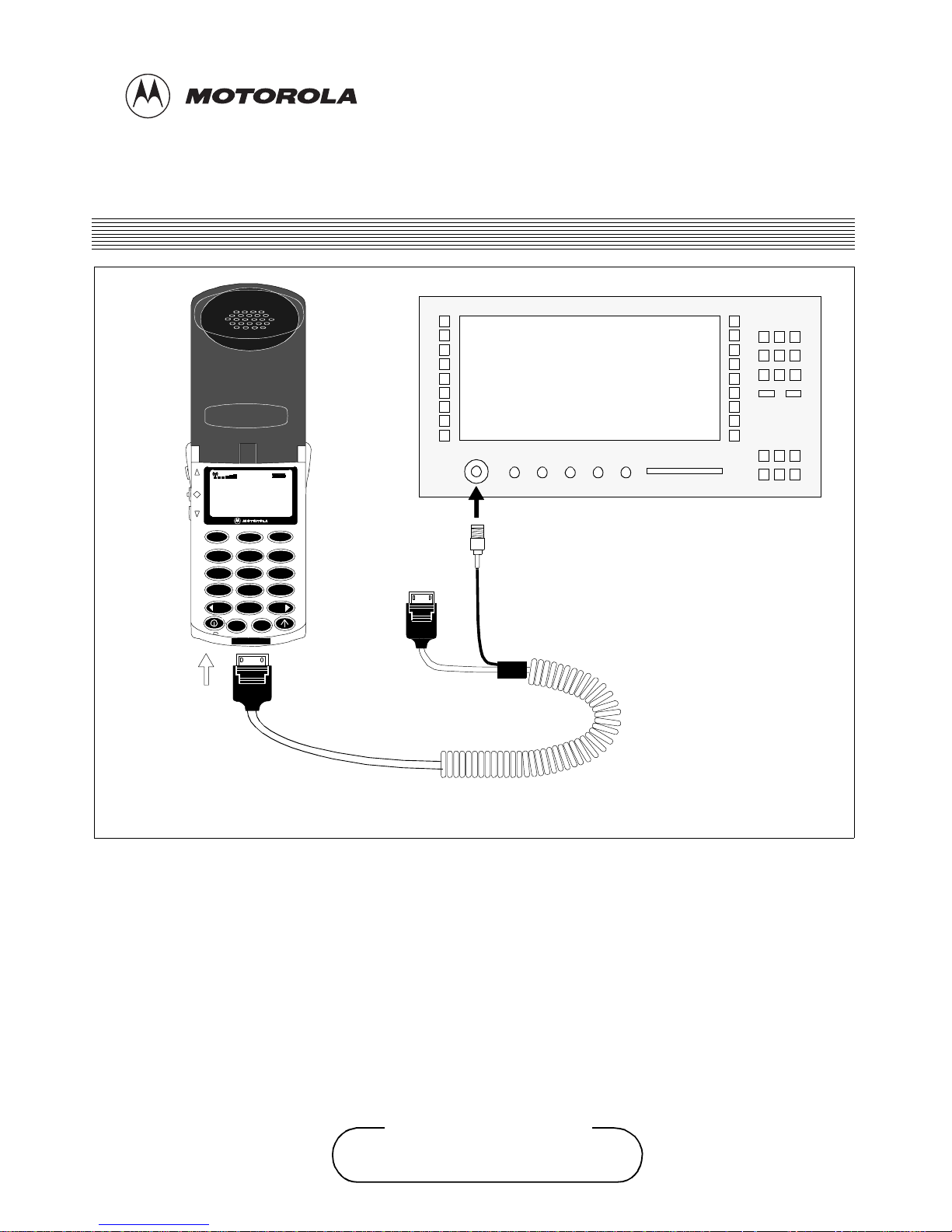
VERIFICATION
1. INTRODUCTION
To test a DCS 1800 StarTAC cellular telephone, to verify
whether or not the unit is functioning correctly, the
following equipment will be required:-
• D.C.S. compatible communications analyser.
• Cable/connector s (SKN4779A) .
• Test SIM card (8102316T01).
• Charged battery pack.
2. EQUIPMENT CONFIGURATION
Initiall y insert th e test SI M card into the slot at the rear of the
personal cellular telephone. If required, further information
on SIM card insertion is available on page 13. Attach the
antenna adapto r t o th e ant enna conne ctor o f th e p hone. Sl ide
a charged battery on to the back of the personal telephone,
so that the telephone can be powered up. Finally, connect a
cable from the test adaptor to the RF in/out port of the
communications analyser, and power both the analyser and
personal telephone on. The equipment set up shown in
Figure 1 should now be in place.
Figure 1: Testing Configuration
D.C..S . COMPATIBLE
COMMUNICATIONS ANALYSER
RF IN/OUT
PORT
32
4 6
5
98
0
c
MR
M+
StarTAC
SMA Plug
OK
MENU
SKN4779A
CABLE
12:00
DEF
MNO
*
#
ABC
JKL
GHI
PQRS
TUV
WXYZ
+
Page 24

DCS 1800 StarTAC CELLULAR TELEPHONE
68P09304A85 DTest4
16 19/07/97
3. TESTING PROCEDURE
All information requ ired to perform the desired t ests and measure ments should be obtained from the communicat ion analyser ’s
user manual.
Ensure that the unit being tested is capable of both initiating a call to the analyser, and receiving a call from the analyser.
Confirm that the displayed Temporary Mobile Subscriber Identity (TMSI), International Mobile Equipment Identity (IMEI),
and dialled number are correct. When a call is in progress th e following tests should be carried out on channels 512, 700
and 885. The record ed results must be within the acceptable stat ed limits, i f t h e un it being te sted passes all the tests it should
be taken as functioning c orrectly. If the unit being tested fai ls to conform with any of the expected measurements, it should be
taken as faulty and repaired accordingly. The following table states the required tests and tolera nces.
TEST TO BE PERFORMED LOWER LIMIT UPPER LIMIT
Transmit average phase error (RMS) at peak power 5
Transmit average phase error (Peak) at peak power 20
Transmit average frequency error at peak power -180 Hz +180 Hz
Transmit power error at level 0 (30 dBm)on CH700 -2 dB +2 dB
Transmit power error at le vel 5 (20 dBm)on CH 700 -3 dB +3 dB
Transmit power error at level 10 (10 dBm)on CH 700 -4 dB +4 dB
Transmit power error at max and min powe r on CH 512 -3 dB +3 dB
Transmit power error at max and min powe r on CH 885 -3 dB +3 dB
Transmit burst mask at max and min power Within DCS specif ication envelope
Receive Bit Error Test for Class II Residual (at -102 dBm)
4
2%
Receiv e Fr ame Erasure Rat e f o r RES II (at -1 02 d Bm )
4
0.12%
Receive level (Rx_LEV) indication at -100 dBm -104 dB -96 dB
Receive level (Rx_LEV) indication at -45 dBm -49dB -41 dB
Receive Quality (Rx_ QUAL) indication for Rx_LEV tests not above 2
Note: 1. The transmit average test values should be derived from 10 separate readings.
2. The receive signal strength for transmit measurements should be -85 dBm.
3. The receive test values should be deri ved from the receptio n of 20K bits of data.
Allow for the loss b etween t he ant enna po rt an d t he RF S MA co nnector on the tes t adapt or . The te st
specifications are written for the power levels at the antenna
Page 25

Customer Services Publishing
Easter Inch, Bathgate, Wes t Lothian
EH48 2EH, United Kingdom
ETrbl5
© Motorola Ltd. 1997All
Rights Reserved
Printed in U.K.
DCS 1800 StarTAC PERSONAL
CELLULAR TELEPHONE
TROUBLESHOOTING
ASSEMBLY REPLACEMENT LEVEL
68P09304A85
19/07/97
17
Cellular Subscriber Group
TROUBLESHOOTING
1. INTRODUCTION
Assembly replacement level troubleshooting and repair of
the DCS 1800 StarTAC personal telephone is limited to
isolation and rep lacement of t he following mai n items only: -
• Antenna
• Battery
• Logic/RF Assembly
• Keypad/Display Board
• Front/Rear Housings
• Keypad Membrane
• Flip Assembly
It is recommended that known good replacement parts and
assemblies be available to be used for troubleshooting by
substitution, and for replacement of parts/assemblies found
to be defective.
If at any time the unit is disassembled, whether repaired or
not, it is rec ommended that a simple t est of maki ng a call an d
checking signal strength and transmit and receive audio
quality is c arried out. Appropr iate action sho uld then be taken
on the outcome of the test.
2. TROUBLESHOOTING AND REPAIR
The troubleshooting information in Table 1 shows some
typical malfunction symptoms and the corresponding
verificatio n and repair procedures. Refer to the disassembly
instruction s located in the disassembly se ction of thi s manual
for instructions on removing and replacing parts/assemblies
from the personal telephone. If the Logic/RF assembly is
replaced a persona lity tran sfer will be necess ary, see page 2 3
for more information.
3. TESTING AFTER REPAIR
After any repair work has been carried out, the unit should
be thoroughly tested to ensure that its operates correctly. This
is especi ally import ant if the Logic/RF assembly is replace d.
For general repairs whi ch do not include repla cing the Logic/
RF assembly, simply placing a call and checking signal
strength, and transmit and receive audio quality is normally
sufficient.
When the Logic/RF assembly is replaced, the unit must have
a comprehensive tes t on a DCScompatible communica tions
analyser. See ‘Testing Procedure’ on page 16 for further
details. The simple test of placing a call on air is usually
carried out on completion of this Test to finalise the testing
procedure.
Additionally, a further audio test “Buzz Test” should be
carried out to eliminate the possibility of transmitter
inter fe r en ce to the au d io path. Ref er to tab le A.
Table A
Command Function
08# Unmute RX audio Path
10# Unmute TX audio path
36# Initiate Acoustic Loopback
434# Change audio Path
477
# Set volume level to 7 max
11700#
Set LO to CH700
1200# Set power level to max
310# Initiate PRS (Starts TX)
01# To terminate test
If any distortion or buzz ing is heard through the earpiec e after
entering the above sequence, refer to the DISASSEMBLY
instructions in this manual and ensure that the earpiece and
microphone are seated correctly and that there is no visible
damage to the display PCB/front housing connector. If no
fault found and symptoms persist replace Logic/RF board
(Table 1, symptom 1c).
Defective Logic/RF assemblies must be replaced
with pre-tested, pre-phased assembl ies.
NOTE
Page 26

DCS 1800 StarTAC CELLULAR TELEPHONE
68P09304A85 ETrbl5
18 19/07/97
1- RF Ground
2- RF In/Out
3- RF Ground
4- Battery Feedback
5- Manual Test Lin e
6- RS232 Tx (Charger & External comms)
7- RS232 Rx (Charger & External comms)
8- Audio In
9- Audio Out / On-Off
10- Battery Ground
11- Uplink
12- Downlink
13- DSC _EN_B
14- External B+
15- Ground
1
15
ThermistorDataB- B+
Figure 1: Main Battery Contacts Figure 2: Auxiliary Battery Contacts
Figure 3: J3 Pin Out
The J3 Butt Pl ug connector has pin outs as listed below. Note th at the pin numbe ring is from ri ght to left a s viewed
from the front of the phone; see above figure.
StarTAC
ThermistorData B- B+
Page 27

TROUBLESHOOTING
ETrbl5 68P09304A85
19/07/97 19
Table 1. DCS 1800 StarTAC Cellular Telephone Troublesh ooting and Repair Chart (Assembly Replacement Le vel).
SYMPTOM PROBABLE CAUSE VERIFICATION AND REMEDY
1. Personal telephone will not turn on
or stay on .
a) Batte ry pack ei ther disc harged
or defec t iv e.
Measure battery voltage across a 50 ohm (>1 Watt) load. If the battery
voltage is <3.25 V dc, recharge the battery using the appropriate battery
charger. If the batte ry will not re c harg e, re pl ace th e ba ttery . If b atte ry is
not at fault, proceed to b.
b) Battery connectors open or
misaligned.
Visually inspect the battery connectors on both the battery assembly and
the portable telephone. Re-align and, if necessary, replace either the
battery or the bat tery connect or assembly. Removing the batte ry connector
assembly has to be don e w ith extre m e c are to a void dam agi ng th e PCB.
If battery con nectors are not at fault, proceed to c
c) Logic/RF Board Assembly
defective.
Remove the Logic/RF Assembly. Substitute a known good assembly and
temporaril y reasse mble th e unit. Depress the PWR button; if un it turns
on and stays on, disconnect the dc power source and reassemble the
telephone wit h the new Lo gic/RF Bo ard assemb ly. Verify that the fault
has been cleared. If the fault has not been cleared then proceed to d.
d) Keypad/Display circuit board
failure.
Replace the Keypad/Display board. Temporarily connect a +3.6 V dc
supply to the battery connectors;(refer to pinouts in the diagram on
previous page). Depress the PWR button; if unit turns on and stays on,
disconnect the dc power source and reassemble the telephone with the
new Ke yp a d/Display boa r d.
2. Personal telephone exhibits poor
reception and/or erratic operation
(such as calls frequently dropping,
weak and/or distorted audio, etc.).
a) An tenna is defective. Check to m ake sure tha t the anten na pin is pro perly conn ected to t he Logic/
RF assembly. If OK, substitute a known good antenna . If the fault is still
present, proceed to b.
b) Logic/RF Board Assembly
defective.
Replace Logic/RF Assembly (refer to symptom 1c). Verify that the fault
has been cleared and re-assemble the unit with the ne w PCB.
3. Display is erratic, or provides
partial or n o disp lay.
a) Mating connections to/from
Keypa d/Display boa r d faulty.
Gain access to Keypad/Display / main board as described in the
DISASSEM BLY instru ctions i n this manual. If con nections a re faul ty
then replace the RF/Lo gic assembly a nd/or the Keyp ad/Display board as
necessary . If connectio ns ar e not at fault, r eplace the original boards a nd
proceed to b.
b) Keypad/Display board is
defective.
Substitute a known good Keypad/Display circuit board, if the fault is not
cleared, re-install the original Keypad/ D isplay PCB and proceed to c.
c) Logic/RF Board Assembly
defective.
Replace Logic/RF Assembly (refer to symptom 1c). Verify that the fault
has been cleared and re-assemble the unit with the ne w PCB.
Repair Chart
Page 28

DCS 1800 StarTAC CELLULAR TELEPHONE
68P09304A85 ETrbl5
20 19/07/97
Table 1. DCS 1800 StarTAC Cellular Te lephone Troublesho oting and Repair Chart (Ass embly Replacement Leve l).
SYMPTOM PROBABLE CAUSE VERIFICATION AND REMEDY
4. Incoming call alert transducer au dio
disto r te d or vo l u m e is too low.
a) Connections to/from Keypad/
Display cir cuit board faulty.
Gain access to Keyp ad/Display board as described in the DISASSEMB LY
instructions in this manual. Check connection to alert transducer. If
connection is not at fault, proceed to b.
b) Alert transducer defective. Gain access to alert speaker (located on the Keypad/Display board) as
described in th e DISAS SEMB LY ins tructio ns in this manual . Unsold er
the alert speake r an d so lder on a known good alert speaker. Place call to
personal tele pho ne from la ndli ne or ot he r mobile /per sona l teleph one and
verify alert signal volume and clarity. If good, re-assemble portable with
new alert speaker. If alert speaker not at fault, re-install original alert
speaker and proceed to c.
c) Logic/RF Board Assembly
defective.
Replace Logic/RF Board Assembly (refer to symptom 1c). Verify that the
fault has been cleared and re-assemble the unit with the new PC B .
5. Personal telephone transmit audio
is weak, (usua lly indicat ed by called
parties complaining of difficulty in
hearing voice from personal phone).
a) Microphone connections to
Keypad/Display board defective.
Gain access to the Microphone as described in the DISASSEMBLY
instructi ons in this manual. Check connect ions and if OK, proceed to b.
b) Microphone defective. Gain access to microphone (located on keypad membrane). Disconnect
and substitute a known good Microphone. Place a call and verify
improvemen t in portable tran smit signa l as heard by called party. If good,
re-assembl e portabl e with new Mic rophone. If Micropho ne is not at fa ult,
re-instal l original Microphone and proceed t o c.
c) Logic/RF Board Assembly
defective.
Replace Logic/RF Board Assembly (refer to symptom 1c). Verify that the
fault has been cleared and re-assemble the unit with the new PC B .
6. Personal teleph one r eceiv e aud io is
weak and/or distorted.
a) Connections to/from Logic/RF
circuit boa rd def ective.
Gain access to Logic/RF board as described in the DISASSEMBLY
instructions in this manual. Check connection and th e f lexistrip from the
earpiece to the Logic/RF circuit board. If connection is not at fault,
proceed to b.
b) Earpiece Speaker defective. Gain access to the earpiece spe aker as described in the DISASSEMBLY
instructions in this manual. Substitute a known good earpiece speaker.
Place a call and verify improvement in earpiece audio. If better,
reassemble the phone with the good earpiece speaker. If it was no better
then re-install the ori gin al com p one nt and proceed to c.
c) Antenna assembly is defective. Attempt a re-phasing of the unit and recheck symptom. If symptom the
same but unit re -phases correc tly, check to make sure th e two antenna
connectors are soldered to the main board correctly and that the antenne
is making good contact with them. If ok, substitute a known good antenna
assembly. If this does not cure the fault , re-install the original assembly
then proceed to d.
d) Logic/RF Board Assembly
defective.
Replace Logic/RF Board Assembly (refer to symptom 1c). Verify that the
fault has been cleared and re-assemble the unit with the new PC B .
Page 29

TROUBLESHOOTING
ETrbl5 68P09304A85
19/07/97 21
Table 1. DCS 1800 StarTAC Cellular Te lephone Troublesho oting and Repair Chart (Ass embly Replacement Leve l).
SYMPTOM PROBABLE CAUSE VERIFICATION AND REMEDY
7. Personal telephone will not
recogniz e/accept SIM card
a) SIM card defective Initially check that t he contacts o n the card a re not dirty ; clean if ne cessary,
and check if fault has been eliminated. If the contacts are clean, insert a
known good SIM card int o the po rtab le telep hon e. Po wer up th e unit and
confirm whet her or not the car d has been accepted . If the fault no longer
exists, the defec tive SIM card should be replaced. If the SIM card is not
at fault, proceed to b.
b) SIM card not being re ad. En su re th at the S IM card is pushed fully h ome in to it ’s recess . If all o k ,
proceed to c.
c) Logic/RF Board Assembly
defective.
Replace Logic/RF Board Assembly (refer to symptom 1c). Verify that the
fault has been cleared and re-assemble the unit with the new PC B .
8. Phone does not sense when flip is
opened or clos ed (usually i ndicated by
inability to a n sw er in c omi ng ca lls by
opening the flip, or ina bility to make
outgoing calls).
a) Magnet in flip defective. Replace fl ip assembl y with known good one (r efer to t he DISASSEM BLY
instructions in this manual. Place call to portable phone and verify ability
to answer by opening flip. If fault still present, replace original flip
assembly and proceed to b.
b) Reed switch defective. Gain acce ss to Keypad/Displ ay board as described in th e DISASSEMBLY
instructions in this manual. Unsolder the reed switch and replace with a
known good one. Re assemble unit. Place cal l to po rtable ph one and verify
ability to answe r by o pening fl ip. If faul t still present , repl ace ori ginal re ed
switch and proceed to c.
c) Keypad/Display board is
defective.
Replace the K eypad/Display board with a known good one. Place call to
portable ph one and v erify t hat the fau lt has be en elimi nated. If not at fa ult,
proceed to d.
d) Logic/RF Board Assembly
defective.
Replace Logic/RF Board Assembly (refer to symptom 1c). Verify that the
fault has been cleared and re-assemble the unit with the new PC B .
9. Vibrator feature not functioning. a) Vibrator motor defective. Replace vibrator motor. If fault still present, replace original vibrator
motor and proceed to b.
b) Logic/RF Board Assembly
defective.
Replace Logic/RF Board Assembly (refer to symptom 1c). Verify that the
fault has been cleared and re-assemble the unit with the new PC B .
10. Internal Charger not wo rking. c) Faulty charger ci rcuit on main
board.
Test a sel ection of batteries in the rear pocket of the desktop cha rger. Che ck
LED display for the charging indications. If these are charging ok, then
the internal charger is at fault. Replace main PCB.
11. Real Time Clock resetti ng when
standard battery is removed.
Lithium button cell in the Flip may
be depleted.
Replace Flip to check. If ok, replace original Flip and replace button
battery.
Page 30

DCS 1800 StarTAC CELLULAR TELEPHONE
68P09304A85 ETrbl5
22 19/07/97
*
PAGE INTENTIONALLY BLANK
Page 31

Customer Services Publishing
Easter Inch, Bathgate, Wes t Lothian
EH48 2EH, United Kingdom
FPers6
© Motorola Ltd. 1997
All Rights Reserved
Printed in U.K.
DCS 1800 starTAC PORTABLE
CELLULAR TELEPHONE
PERSONALITY TRANSFER
68P09304A85-O
19/07/97
23
Cellular Subscriber Group
PERSONALITY TRANSFER
4. INTRODUCTION
Personality Transfers are required when a phone is Express
Exchanged or when the main board is replaced. The
different variations (languages, features) of the DCS
starTAC personal cellular telephones requires that each
main board must be configured correctly to ensure that the
unit takes on the correct personality required. Therefore,
when a main board is replaced its personality must be
transferred into the new board, so that it functions correctly
in the customers unit. There are two possible methods of
transfer.
• Normal Transfer, an d;
• Mas ter Transf er
If the defective unit powers up, then the Normal Transfer
method should be followed. If the faul ty unit will not power
up, then a Master transfer will be required to configure the
replacement board, once installed.
5. NORMAL TRANSFER
This method allows the personality, selected features and
stored phone numbers of a defe ctive radio, to be transfe rred
into a repair ed radio. Data is transferr ed from the donor unit
into the recipient unit using a Transfer card (Part No
5104025D01). The instruction steps should be followed in
order.
Step 1. Insert the Transfer card into the slot located on
the back of the donor unit. Turn the donor unit
on, the display should show ‘Clone’.
Step 2. The donor unit is now in the cloning mode, and
ready to transfer the first block of data.
Step 3. E nter 021# via t he unit’s keypa d. This comman d
will cause the first block of information to be
uploaded into the Transfer card.
Step 4. While data transfer is taking place between the
unit and the card, ‘Please Wait’ will be
displayed. After a short period of time, if the
data transfer has been completed correctly,
‘Clone’ will re-appear in the donor unit’s
display.
Step 5. When the first data block has been successfully
uploaded, remove the card from the donor.
Step 6. Insert the Transfer card into the slot located on
the back of the recipient unit. Turn the recipient
unit on, the display should show ‘Clone’.
Step 7. The recipient unit is now in the cloning mode,
and ready to receive th e first block of data.
Step 8. Enter 03# via the unit’s keypad. This command
will cause th e recipient unit to download the first
data block from the Transfer card.
Step 9. While data transfer is taking place between the
card and the unit, ‘Please Wait’ will be
displayed. After a short period of time, if the
data transfer has been completed correctly,
‘Clone’ will re-appear in the recipient unit’s
display.
Step 10. The second data bloc k m ust now be transferred.
Repeat steps 1 to 9, but enter 022# to program
the second data block into the Transfer ca rd.
Step 11. The third data block must now be transferred.
Repeat steps 1 to 9, but enter 025# to program
the third data block into the Transfer ca rd.
Step 12. When the third block of data has been
transferred successfully, remove the Transfer
card and check the repaired radio functions
correctly. See page 19 for further informati on.
Page 32

68P09304A82-O FPers6
24 1/9/97
68P09304A85-O FPers6
24 19/07/97
DCS 1800 starTAC CELLULAR TELEPHONE
6. MASTER TRANSFER
This method of transfer should only be followed when the
defective unit will not power up, or complete a Normal
Transfer. As mentioned earlier, there may be different
variations (OEM looks for example) of the Motorola DCS
starTAC cellular telephone, each model requiring the main
board to be configured differently for correct operation.
When carrying out a Master Transfer it is not possible to
transfer the customers selected features or stored phone
numbers, only the model personality can be programmed
into the repaired unit.
Each different version of the DCS starTAC cellular
telephone, requires its own Master Transfer card which
contains essential set up information. Master SIM cards may
be ordered pre-programmed, or created from a Normal
Transfer card. The instruction steps should be followed in
order.
Step 1. Select the requi red M a st er SI M car d .
Step 2. Insert the Master Transfer card into the slot
located on the back of the repaired unit . Turn the
unit on, the display should show ‘Clone’.
Step 3. Enter 03# via the unit’s keypad. This command
will cause the configuration data to be
downloaded from the Maste r Transfer card.
Step 4. While data transfer is taking place between the
card and the unit ‘Please Wait’ will be
displayed. After a short period of time, if the
data transfer has been completed correctly,
‘Clone’ will re-appear in the recipient unit’s
display.
Step 5. When the data block has been transferred
succes sfully, remove t he Master Trans fer card
and check the radio functions correctly. See
page 19 for details.
At no point should either 021#, 022# or 025# be entered
while a Master Transfer card is in the radio. If either of the
stated co mmands are entered, the master information on the
card will be erased. To pr event the above happening the car d
can be locked by entering 06# via the unit’ s keypad, with the
card inserted. Unlock the card by entering 07#.
Note: If during ei ther transfer process a pr oblem arises, an
error message will be displayed. If the Transfer card
is removed before the data transfer is completed
‘Bad Data on Card’ will appear in the display. If
either situation arises, the process should be
repeated.
7. MASTER SIM CARD CREATION
When required a Master SIM card can be created by:-
Step 1. Insert a Transfer card into a unit which is
already configured in the desired way. Turn the
unit on, the display should show ‘Clone’.
Step 2. E nter 024# via t he unit’s keypa d. This comman d
copies the personality information in the unit
onto the Transfer card to create a Master
Transfer card.
Step 3. While data transfer is taking place between the
unit and the card ‘Please Wait’ will be
displayed. After a short period of time, if the
data transfer has been completed correctly,
‘Clone’ will re-appear in the recipient unit’s
display.
Step 4. A Master Transfer card has now been crea ted.
Lock th e c ar d to p r ev e nt acciden t al in f o rm at i on
erasure (see previous section). Remove the card
from the unit, and stor e until required.
Page 33

Customer Services Publishing
Easter Inch, Bathgate, Wes t Lothian
EH 48 2 EH, United Kingdom
GDis7
© Motorola Ltd. 1997
All Rights Reserved
Printed in U.K.
DCS 1800 StarTAC PERSONAL
CELLULAR TELEPHONE
DISASSEMBLY
68P09304A85
19/07/97
25
Cellular Subscriber Group
DISASSEMBLY INSTRUCTIONS
1. INTRODUCTION
The DCS 1800 StarTAC cellular telephone is assembled
using a simple slide and press fit between front and back
housings followed by positioning of two fixing screws. The
antenna does not have to be removed before disassembly is
started, the antenna can be removed when the back panel is
free. Reaso nable care should be taken duri ng the di sassembly
and reassembly of the unit in order to avoid damaging or
stressing the housing and internal components. Ensure that a
properly grounded high impedance conductive wrist st rap is
used while performi ng these procedures on elec tronic units.
2. RECOMMENDED TOOLS
The following tools are recommended for use during the
assembly/disassembly of the personal telephone.
• Anti-Static Mat Kit 0180386A82; includes:
— Anti-Static Mat 66- 80387A95
— Ground Cord 66-80334B36
— Wrist Band 42-80385A59
• Plastic Bladed Tool (SLN7223A
Many of the inte grated circuit devi ces used in this
equipment are vulnerable to damage from static
charges. E nsure t hat adequa te st atic pr ote ction is
in place when handling, shipping, and servicing
CAUTION
•Τ6 Torx Screw Driver
• Antenna Removal Tool (SYN5179)
• A small flat bladed screw driver,
3. DISASSEMBLY PROCEDURE
3.1 DISASSEMBLY PROCEDURE
The following information describes the procedure for
removing and accessing various parts of the DCS1800
StarTAC.
4. ASSEMBLY PROCEDURE
Once the unit is disassembled and the repair is carried out it
then becomes obvious that to assemble the unit, the
procedure is the reverse of that previously completed for
disassembly. Note that the housings must be securely held
together and the screws torqued appropriately for assembly.
Failure to secure the housings properly could result in
possible damage.
Refer to the mechanical exploded view on
page 38, as necessary, while performing the
disassembl y/assembly procedures.
NOTE
Page 34

DCS 1800 StarTAC PERSONAL CELLULAR TELEPHONE
68P09304A85 GDis7
26 19/07/97
Carefully unscrew both Torx Screws with a
size 6 dr i v er.
1
Push Rear housing from the bottom upwards towards the antenn a; when
the housi ng slides free, allow the a ntenna to remain in the rear housing
2
Page 35

DISASSEMBLY
GDis7 68P09304A85
19/07/97 27
2
The two housings simpl y come apart and t he antenna can remain in th e
back housing or you can carefully extract it from the retaining clips.
3
Unclip the flexistrip retaining bar with either a
plastic tool or a fine scredriver.
4
Page 36

DCS 1800 StarTAC PERSONAL CELLULAR TELEPHONE
68P09304A85 GDis7
28 19/07/97
Withdraw the Flexistrip cable from the main PCB.
Pry the c ircuit bo ard asse m b ly ou t w ith the P la stic tool
or small screwdriver until it comes away completely.
6
5
Page 37

DISASSEMBLY
GDis7 68P09304A85
19/07/97 29
The Display / Keypad board just pulls away from
the Main board assembly.
7
Unclip the antenna guide from two gold retaining clips and gently ease
towards you, making sure that the tube is still attatched to the foil.
8
Page 38

DCS 1800 StarTAC PERSONAL CELLULAR TELEPHONE
68P09304A85 GDis7
30 19/07/97
Pull the f oi l s trip to war ds y ou a nd force it al l th e wa y ov er unt ill you can see
the black adhesive str ip which covers t he reverse sid e of the board.
9
Turn the c ir cuit bo ar d o ver a nd pul l t he blac k a hes iv e st ri p off
completely, leaving the foil strip attatched.
10
Page 39

DISASSEMBLY
GDis7 68P09304A85
19/07/97 31
You now have access to both si des of the circuit board ; this is the
Audio/Di gital side.
11
This side is mostly RF.
12
Page 40

DCS 1800 StarTAC PERSONAL CELLULAR TELEPHONE
68P09304A85 GDis7
32 19/07/97
Take up the Flip and remove the Keypad
Membrane.
13
Prize off the adhesive backed cover plate with the
small screwdriver or plastic tool.
14
Page 41

DISASSEMBLY
GDis7 68P09304A85
19/07/97 33
With a small screwdriver or a pair of tweezers, ease the tab
of the central Flexistrip guard out and over the clam shell .
15
With a small screwdriver , locate the recess on the right hand
side of the clam shell and slide the locking pin to the left.
16
Page 42

DCS 1800 StarTAC PERSONAL CELLULAR TELEPHONE
68P09304A85 GDis7
34 19/07/97
Then ease the complete cl am shell off of the display/
keypad housing.
17
18
Remove the flip cover by pushing the retaining
pins and lifting the cove r.
Page 43

DCS 1800 StarTAC PERSONAL CELLULAR TELEPHONE
68P09304A85 GDis7
35 19/07/97
19
Lifti ng the c ove r away g ives acces s to th e spe aker,
batery and vibrator.
Page 44

DCS 1800 StarTAC PERSONAL CELLULAR TELEPHONE
68P09304A85 GDis7
36 19/07/97
6
1
16
7
23
2
22
20
19
18
3
15
14
8
24
9
12
25
5
?
10
17
13
Page 45

DISASSEMBLY
GDis7 68P09304A85
19/07/97 37
REPLACEMENT PARTS LIST
Reference No. PART No DESCRIPTION
1 0309333C01 SC REW TRILOB E W/CAP WASHER
2 0509220D01 GROMMET MIC
3 0509221D01 GROMMET ALERT
4 1109155J01 ADHESIVE DCA COVER (not shown)
5 1509237S01 HSNG FLEX COVER
6 2609231D02 SHIELD LOGIC
7 3709262J01 TUBE ANTENNA
8 3809105S01 ACTR KYPD 19 KEY
3809170E01 ACTR KYPD 17 KEY
9 4709050R01 SHAFT DCS RIGHT
10 5009536H15 MIC LEADED W/PINS
11 5409150R01 LABEL FLEX
12 5509242E01 HINGE DCS
13 7509165R01 PAD SHOCK
14 8509173J01 ANT DIRECT CONN 1800MHZ
15 4009106S01 SW KYPD METAL DOME 19 POS
4009293D01 SW KYPD METAL DOME 17 POS
16 7209185S01 19 KEY DISPLAY BOARD
(complete apart from keypad domes)
7209147D01 17 KEY DISPLAY BOARD (complete apart from keypad domes)
17 2809454C02 32 PIN CONNECTOR (MAIN)
18 4009060E01 SW TACTILE SMD
19 5009473S01 ALERT EM 5V SMD
20 0909449B01 15 Pin Accessory Connector
21 4009169E01 SIM card contact s (not s hown)
22 0 109194S01 F RONT HOUSING 19 KEY
0109212D01 FRONT HOUSING 17 KEY
23 0109284S01 REAR HOUSING
24 0109322D03 ASSY LENS “Motorola”
25 0109485D01 ASSY HSNG MAIN FLIP BLK (Blank Escutcheon)
3309284K01 “Motorola” metal escutcheon (outside of flip)
5409184R55 “StarTAC” vi nyl escutcheon
5409184R79 “EPlus” vinyl escutcheon
5409184R81 “Bouyges” vinyl escutcheon
REPLACEMENT PARTS LIST FOR DCS 1800 Star TAC
Page 46

DCS 1800 StarTAC PERSONAL CELLULAR TELEPHONE
68P09304A85 GDis7
38 19/07/97
*
PAGE INTENTIONALLY BLANK
Page 47

Customer Services Publishing
Easter Inch, Bathgate, Wes t Lothian
EH48 2EH, United Kingdom
HAcc8
© Motorola Ltd. 1997
All Rights Reserved
Printed in U.K.
68P09304A85
19/07/97
39
Cellular Subscriber Group
DCS 1800 StarTAC PERSONAL
CELLULAR TELEPHONE
ACCESSORIES
RECHARGABLE BATTERY PACKS
(GENERAL)
1. INTRODUCTION
The DCS StarTAC normal ly opera tes from a 3.6V d c batt ery
pack. There are a number of battery packs, with various
options offered as standard, depending on the market
requirements;
(i) The Slim Lithium E•P Battery (SNN4667).
(ii) The Light LiIon E•P Battery (SNN4785).
(iii) The Slim NiMH E•P Batte ry (SNN4669).
(iv) The Extra Capacity LiIon E•P Battery
(SNN4668).
(v) The Slim LiIon E•P Batt ery (SNN4867)
Full specifications are given in the table below.
* NOTE: For Auxi liary Ba tter ies, t he wei ghts and volum es give n are
for the batteries only. The Talk and Standby times are in addition
to any main ba tte ry fitted .
Each battery pack is housed in a polycarbonate case, which
provides superior impact resistance. Removal of the battery
pack is accomplished through a quick-release latch. If
required, the User Guide contains information on removing
and replacing the battery packs.
2. RECHARGING
The DCS StarTAC has a built in rapid charger. The internal
charger can be powered by either the Travel Charger or the
Cigarette Lighter Adaptor. Both these accessories can power
the phone for a telephone call or
fast-charge a discharged
battery (but not both simultaneously).
Batteries can also be charged directly by the Desktop Rapid
Intellicharge.
Table 1: Battery Specifications
Battery
Information
Main(Primary ) Batteries Auxilliary Battery
Battery Slim LiIon Light LiIon Slim NiMH Extra Capacity
LiIon
Slim LiIon Auxi lliary
Weight (grams)
(phone plus battery)
110 98.5 125 126.5 130
Volume (cc) (phone
plus batt e r y)
100 100 135 109.4 145
Talktime (mins)
(approx.)
100 - 140 60 - 90 100/120 180 - 280 170 - 260
Stand-by time
(hours) (approx.)
30 - 40 20 - 25 30/40 60 - 75 55 - 70
Capacity (mA/Hours) 500 350 500 900 900
Charge Time (Hour s ) 2.5 2.5 1.0 2.5 2.5
Page 48

DCS 1800 StarTAC PERSONAL CELLULAR TELEPHONE
68P09304A85 HAc c8
40 19/07/97
1. (“EXPERT PERFORMANCE”)
BATTERIES AND CHARGERS
E•P batteries are marked with th e new E•P logo and cont ain
an EPROM which provides data to E
•P telephones or E•P
chargers. This data characterizes the battery’s charging
characteristics, such as preferred fast charge and trickle
charge current. This means that E
•P batteries can be used
and charged in the most efficient way for maximum
performance.
The critical chargin g parameters are stored in a 128 x 4 serial
EPROM in the battery, which the charging device reads at
the start of the charging cycle. If the EPROM is not detected
(for non-E
•P batteries ) then default charging valu es are used.
As well as E
•P batteries, E•P products include the cigarette
lighter adaptor/charger and the E
•P IntelliCharger. Any
product with the E
•P symbol is capable of either providing
E
•P data or interpret ing it.
No repairs can be carrie d out on any of the battery packs . If
a rechargeable battery pack becomes defective, it should be
replaced.
2. BUILT IN E•P BATTERY FA ST
CHARGER
All DCS StarTACs contain a built in E•P battery charger
which can charge any battery attached to the phone . The
charge r can also re ad the data f rom the E•P batteries fo r
optimum charging performance with t hat particular battery.
The built in charger obtains its power from either the
Cigarette Lighter Adaptor or the Travel Charger. Both
supplies mo nitor the batt ery feedback line to provide optimal
supply voltag e.
When the phone is at tache d t o a cha rgi ng devic e, t he batte ry
icon flashes to i ndicat e cha rging is ta king place . The batte ry
icon bars indic ate the approximate state of charge; thre e bars
indicating a charge capacity of 95% or more. When attached
to a charger, the displ ay shows a flashing ba ttery and bat tery
level even if the phone is switched off.
Note that battery charging is suspended while the phone is
in a call (because of the extra current demand), but the battery
icon will stil l continue to flash.
Page 49

Cellular Subscriber Group
DCS 1800 StarTAC PERSONAL
CELLULAR TELEPHONE
ACCESSORIES
Ni MH BATTERY PACKS
Customer Services Publishing
Easter Inch, Bathgate, West Lothian
EH48 2EH, United Kingdom
HAcc8
© Motorola Ltd. 1997
All Rights Reserved
Printed in U.K.
68P09304A85
19/07/97
41
RECHARGEABLE BATTERY
PACKS
1. INTRODUCTION
The DCS 1800 StarTAC can operate from a 3.6V dc Nicke l
Metal Hydride rechargeable battery pack. The Standard
NiMH has a capacity of 500mA-hours. The dimensions are
42 mm (L) x 51 mm(W) x 13 mm(D) and the contact
configurati on of the ba ttery pack is shown in figure 1.
Removal of the battery pack is accomplished through a
quick-release latch. If required refer to the ‘Disassembly
Instructions’ in this manual, for battery pack removal and
replacem ent information.
Figure 1. Rechargeable Battery Pack Dimensions and Connections
STANDARD NiMH & Case
500 mA-Hour
Thermistor
B+
B-
Data
Page 50

DCS 1800 StarTAC PERSONAL CELLULAR TELEPHONE
68P09304A85 HAc c8
42 19/07/97
*
PAGE INTENTIONALLY BLANK
Page 51

DCS 1800 StarTAC PERSONAL
CELLULAR TELEPHONE
ACCESSORIES
Li Ion BATTERY PACKS
Cellular Subscriber Group
Customer Services Publishing
Easter Inch, Bathgate, Wes t Lothian
EH48 2EH, United Kingdom
HAcc8
© Motorola Ltd. 1997
All Rights Reserved
Printed in U.K.
68P09304A85
19/07/97
43
RECHARGEABLE BATTERY
PACKS
1. INTRODUCTION
The DCS 1800 StarTAC can operate from two types of
standard 3.6V dc Lithium Ion rechargeable battery packs,
and one auxiliary (see next page). The Slim LiIon has a
capacity of 500mA-hours with dimensions 42 mm (L) x 51
mm(W) x 8 mm(D), and the Standard Extra Capacity LiIon
has a capacity of 950mA-hours with dimensions 42 mm (L)
x 51 mm(W) x 13 mm(D). The contact configuration of the
battery packs is shown in figure 1.
Removal of the battery pack is accomplished through a
quick-release latch. If required refer to the ‘Disassembly
Instructions’ in this manual, for battery pack removal and
replacem ent information.
SLIM LiIon
500 mA-Hour
Thermistor
Figure 1. Rechargeable Battery Pack Dimensions and Connections
B+
B-
Data
STANDARD XT LiIon & Case
950 mA-Hour
Page 52

DCS 1800 StarTAC PERSONAL CELLULAR TELEPHONE
68P09304A85 HAc c8
44 19/07/97
*
PAGE INTENTIONALLY BLANK
Page 53

Cellular Subscriber Group
Customer Services Publishing
Easter Inch, Bathgate, Wes t Lothian
EH48 2EH, United Kingdom
HAcc8
© Motorola Ltd. 1997
All Rights Reserved
Printed in U.K.
68P09304A85
19/07/97
45
DCS 1800 StarTAC PERSONAL
CELLULAR TELEPHONE
ACCESSORIES
AUXILIARY BATTERY PACK
Thermistor
B+
B-
Data
RECHARGEABLE BATTERY
PACKS
1. INTRODUCTION
The DCS 1800StarT AC can operate from an auxiliary 3.6V
dc Lithiu m Ion rechar geable batt ery pa ck , whic h can be a lso
be used in conjunction with one of the standard batteries.
The Auxiliary LiIon has a capacity of 950mA-hours with
dimensions 92 mm (L) x 46 mm(W) x 12 mm(D) (not
including lugs). The contact configuration of the battery
pack is shown in figure 1.
Removal of the battery pack is accomplished through a
sprung latch. Th e batt ery c ontac ts ar e disc onnec ted unti l t he
latch is extended, i.e. as the battery is when fitted. If
required refer to the ‘Disassembly Instructions’ in this
manual, for battery pack removal and replacement
Figure 1. Rechargeable Battery Pack Dimensions and Connections
AUXILIARY LiIon & Case
950 mA-H ou r
Page 54

DCS 1800 StarTAC PERSONAL CELLULAR TELEPHONE
68P09304A85 HAc c8
46 19/07/97
*
PAGE INTENTIONALLY BLANK
Page 55

DCS 1800 StarTAC PERSONAL
CELLULAR TELEPHONE
ACCESSORIES
™
RAPID DESKTOP CHARGER
Cellular Subscriber Group
Customer Services Publishing
Easter Inch, Bathgate, Wes t Lothian
EH48 2EH, United Kingdom
HAcc8
© Motorola Ltd. 1997
All Rights Reserved
Printed in U.K.
68P09304A85
19/07/97
47
E•P RAPID DESKTOP CHARGER
1. DESCRIPTION
The DCS StarTAC Desktop Charger is a dual pocket,
intelligent charger capa ble of charging batteries of different
technologie s and capac ities automa tically. The charger re ads
the charging parameters from any E•P compati ble batt ery or
uses default charging values if a battery EPROM is not
detected.
A micro cont rol ler i nside of the char ger contr ols the charg ing
current delivered to the rear pocket according to its stored
program and the values of the charging variables read from
the battery pack. The input voltage to the charger is provided
by the Rapid Charging Transformer which acts as a voltage
tracking power supply.
The front pocket of the charger is capable of powering a
StarTAC and its internal charger to allow charging of any
attached primary and/or auxiliary batteries. The rear pocket
can charge any stand alone StarTAC batteries .
2. MODEL COMPLEMENT
E•P Rapid Charger Base SPN4425
3. OPERATION
The charger communica tes with an a ttached ph one using t he
interface connecto r .
Figure 1. Rapid Desktop Char ger
Page 56

DCS 1800 StarTAC PERSONAL CELLULAR TELEPHONE
68P09304A85 HAc c8
48 19/07/97
If the phone is chargi ng or trans mitt ing , the deskt op charge r
will take lower prior ity usage of the power supply. While the
phone is char ging an at tached batte ry, the phon e contr ols the
Battery_Feedback line, which is routed from the phone to
the Transformer. This is so the Transformer can supply the
correct volta ge (battery voltage + 1. 4V), through the charger,
and into th e p hone. Whe n the phone i s not in the charg ing or
transmit mode it allows the charger base to take control of
the Battery_Feedback so the Transformer can supply the
corre ct voltage to any batt er ies in the charger’ s rear pocket.
The char ger s ens es a bat ter y ins tal led in the r ear pock et by
measuring the battery’s terminal voltage and the battery’s
thermistor resistance. The thermistor characteristics for all
batteries is shown in the Charge r Specifica tions Table. If th e
charger sees an open circuit on the thermistor line, the
pocket’s LED will re main off indi cating no batt ery detect ed.
Upon insertion of a battery, the charger will attempt to rea d
the batt ery EPR OM to deter mine the ty pe of ba tter y and it’s
charging characteristics. The battery is given up to three
requests for data. If the charger determines that no EPROM
is present, default charging values are us ed for high capacit y
and low capacity type batteries (a low capacity battery has
its Data pin floating and a high capacity has its Data pin
grounded).
If after the third data request the charger still receives
corrupted data, the battery will be classified as faulty. The
battery will also be classified as faulty if its voltage falls
below 0.5V while under cha rge (the batt ery is assumed to be
shorted).
1. LED INDICATORS
The charger base ha s three bico lour LED’s whic h can be off,
green, or red. The front LED indicates the charge status of
any primary battery attached to the phone; the middle LED
indicates the charge status of any auxiliary battery attached
to the phone; and the back LED indicates the charge status
of any battery located in the rear pocket.
The charge status is indi cate d by the followi ng LED states :-
Off: Battery pocket is inactive. Battery
unchargeable or battery thermistor
cannot be detected.
Flashing Yellow: Battery is waiting to rapid charge (i.e.
another battery is charging, the batt ery is
out of temperature range or below
voltage, or t he transceiver is t ransmitting.
Flashing Red: Shorted battery, open battery contact,
corrupted EPROM data, or Lithium
battery in overvol tage mode.
Solid Red: Battery is being rapid charged.
Solid Green: Charge cycle is complete (battery is
>90% of rated capacity, trickle charge
may be activated.
Note 1/ The LED colour does not change when
the phone is in a call.
Note 2/ The charger waits 11 seconds before it
switches the rear L ED t o fl ashing yel low
after receivin g a message fr om the pho ne
that it is transmitting. This is to prevent
the charger from flashing yellow when
the phone auto-registers.
Note 3/ The flashing rate for all LED’s is 1 Hz.
2. MAINTENANCE
The Desktop Charger is considered non-serviceable. If it
becomes faulty, it s hould be replaced with a new one.
SPECIFICATIONS - DESKTOP RAPID CHARGER
Operating Temperature Range 0°C to +50°×C
Storage Temperature Range −40°C to +85°×C
Input Current (max) 1.1 Amps
INPUT VOLTAGE
Battery Voltage:
0 - 3.0V dc
3.0 - 5.1V dc
>5.1V dc
Charger Input Voltage:
4.4V dc
(Vba tt + 1.4V) dc
6.5V dc
THERMIST OR CHAR ACT ERIS T ICS
Temperature:
+5°×C
+25°×C
+40°×C
+45°×C
Resistance:
25.400 + 1270 O hms
10,000 +
500 Ohms
5,330 +
266 Ohms
4,370 +
218 Ohms
Page 57

DCS 1800 StarTAC PERSONAL
CELLULAR TELEPHONE
ACCESSORIES
RAPID CHARGING TRANSFORMER
Cellular Subscriber Group
Customer Services Publishing
Easter Inch, Bathgate, Wes t Lothian
EH48 2EH, United Kingdom
HAcc8
© Motorola Ltd. 1997
All Rights Reserved
Printed in U.K.
68P09304A85
19/07/97
49
RAPID CHARGING TRANSFORMER
1. DESCRIPTION
The Travel Battery Charger is essentially a mains transformer
and rectifier. It provides DC power to operate an attached
DCS StarTAC as well as providing power to the phone’s
internal charger circuit. If no battery (or a dead battery) is
attached to the phone, the transformer can supply sufficient
current for full phone operation. The same Transfo rmer is also
used to supply power to the E•P Rapid Desktop Charger.
The charger unit is designed to track 1.4 Volts above the
phone’s attached battery during charging, within a certain
range. Var ious mai ns plug styles can be at tache d to the ma in
transformer unit for different market requirements.
The charger has a length of cable with a plug termination
which fits into the accessory/charger socket at the base of
the DCS StarTAC.
Figure 1. E•P Rapid Charging Transformer.
Page 58

DCS 1800 StarTAC PERSONAL CELLULAR TELEPHONE
68P09304A85 HAc c8
50 19/07/97
1. MODEL COMPLEMENT
The main transforme r unit has been design ed to operate from
a wide range of supply voltages (see specs below) and is
common to all countries. Because of this it has several
adaptors to allow for different physical connection to the
mains su ppl y . Th e Eu r o pe an v er si on s ar e :
Travel Charger Transformer SPN4278
Travel Charger Adaptor (UK) SPN4656
Travel Charger Adaptor (Euro) SPN4655
2. OPERATION
A green LED on the transf ormer indicates that mai ns power
is switched on. When the phone is attached to a charging
device, the battery icon in the phone’s display flashes to
indicate charging is taking place. The battery icon bars
indicate the approximate state of charge; three bars
indicating a charge capacity of 90% or more . When attached
to a charger, the displa y shows a flashing bat tery and batt ery
level even if the phone is switched off.
3. MAINTENANCE
The Travel Charger is considered non-serviceable. If it
becomes faulty, it s hould be replaced with a new one.
SPECIFICATIONS - RAPID CHARGER TRANSFORMER
Operating T e mper ature Range 0°C to +50°×C
Storage Temperature Range −40°C to +85°×C
Input Voltage 90 - 264V ac
Input Frequency 50 - 60 Hz
OUTPUT VOLTAGE
Battery Voltage:
0 - 3.0V dc
3.0 - 5.1V dc
>5.1V dc
Charger Output Voltage:
4.4V dc
(Vba tt + 1.4V) dc
6.5V dc
Output Cu rrent 0 - 1.1 Amp (cont inuous), 1.6Amp (peak)
Ripple <50mV p-p @ <10K H z
<30mV p-p @>
10KHz
Maximum Short Circuit Curr e nt 2 Amps
Page 59

Customer Services Publishing
Easter Inch, Bathgate, Wes t Lothian
EH48 2EH, United Kingdom
HAcc8
© Motorola Ltd. 1997
All Rights Reserved
Printed in U.K.
68P09304A85
19/07/97
51
DCS 1800 StarTAC PERSONAL
CELLULAR TELEPHONE
ACCESSORIES
™
CIGARETTE LIGHTER ADAPTOR/CHARGER
Cellular Subscriber Group
E•P CIGARETTE LIGHTER
ADAPTOR/CHARGER
1. DESCRIPTION
The cigarette lighter adaptor/charger allows a DCS StarTAC
to op erate usi ng a vehi cle’s el ectri cal syst em. I t s impl y plu gs
into a cigarette lighter socket and has a length of coil chord
attached which appli es power to th e accessor y conne ctor on
the phone. A regulator inside the adaptor reduces the
vehicle’s ba ttery vol tage down to 1. 4 volts abo ve the phone’s
internal battery voltage, within a certain range.
The adaptor can power the phone for call operation even if
the phone’s battery is fully discharged. It also supplies DC
power to fast c harge a ba ttery when the phon e is not in a call,
but cannot do both at the sa me time.
Figure 1. E•P Cigar ette Lighter Adaptor/Charger (ULTRA SAVER)
Page 60

DCS 1800 StarTAC PERSONAL CELLULAR TELEPHONE
68P09304A85 HAc c8
52 19/07/97
An LED is located on the mai n body of the adaptor to indicat e
that it is correctly inserted into the cigarette lighter socket
and that DC is applied. The Travel Cha rger m onitors the
battery feedbac k line (pin 4) on the external conne ctor of the
phone to provide the required supply voltage.
1. MODEL COMPLEMENT
One version covers all normal vehicle applications:
Cigarette Lighter Adaptor/Charger SYN4241
2. OPERATION
A green LED on the body indicates DC power is applied.
When th e ph one is atta ch ed t o a ch ar gi ng d evi ce , t he bat te ry
icon in the phone’s display flashes to indicate charging is
taking place. The battery icon bars indicate the approximate
state of charge; three bars indicating a charge capacity of
90% or more. When attached to a charge r, the display sho ws
a flashing battery and battery level even if the phone is
switched off.
3. MAINTENANCE
A 2.0 A glass tube fuse is located in the tip of the adaptor.
Unscrew the tip to gain access if su spect. Apart from the fuse,
the adaptor is considered non-serviceable. If it becomes
faulty, it should be re placed with a new one.
SPECIFICATIONS - CIGARETTE LIGHTER ADAPTOR
Operating T e mper ature Range −30°C to +60°×C
Storage Temperature Range −40°C to +85°×C
Input Voltage 10.8 - 33V dc
Input Current (at 13.6V dc input) No Load: 25mA
At 1.6A lo ad: 960 m A
OUTPU T VOLTAGE
Battery Voltage:
0 - 3.0V dc
3.0 - 5.1V dc
>5.1V dc
Charger Output Voltage:
4.4V dc
(Vba tt + 1.4V) dc
6.5V dc
Output Current 0 - 1.0 Amp (continuous), 1. 6A mp ( peak)
Ripple <30mV peak to peak
Maximum Short Circuit Curr e nt 2 Amps
Page 61

DCS 1800 starTAC PERSONAL
CELLULAR TELEPHONE
ACCESSORIES
CAR KITS
Cellular Subscriber Group
Customer Services Publishing
Easter Inch, Bathgate, Wes t Lothian
EH48 2EH, United Kingdom
JMCK10
© Motorola Ltd. 1997
All Rights Reserved
Printed in U.K.
68P09304A85-O
19/07/97
53
CAR KIT
1. INTRODUCTION
The DCS StarTAC uses a dedicated car kit that has been
designed for use with the StarTAC range of personals. The
kit offers full duplex handsfree operation and external
power, which allows it to be used in the vehicle with no
drain on the phone’s battery. It also provides rapid char ging
of an attached battery via the phones internal charging
circuitry
This kit, has a direct antenna connector (antenna not
supplied) and fully functional Smart Handset. The Handset
provides the user with the following features:
• Illuminated keypad and display.
• Retrieve and store the Phone Book entry lis t.
• Access to all the StarTAC’s features and functions.
As this kit has been specifically designed for use with the
StarTAC, it is not backward compatible with any other
DCS product.
Car Kit S5338
2. INSTALLATION
The installation for th e StarTAC car kit can be found on the
following pages.
Page 62

DCS 1800 starTAC CELLULAR TELEPHONE
68P09304A85-O JMCK10
54 19/07/97
1. INSTALLATION INTRODUC TIO N
The Motorola StarTAC Car Kit provides the user with
the capability of usi ng their persona l phone with full handsfree operation whilst in a vehicle. The StarTAC Car Kit
provides power to the transceiver unit and allows rapid
charging for any rechargeable battery attached to the
phone.
When in the Car Kit the transceivers antenna is
automatically disconnected, and the RF routed via the RF
coaxial cable to an external antenna to enhance reception.
All of the phones functions are accessible via the Smart
Handset keypad.
When calls are placed, your unit will automatically enable
hands free operation. To make a hands free call, leave the
phone in the cradle, enter the number (or recall it from
memory), using the smart handset, then press OK.
To receive a call in hands free, simply press the OK button
of the handset. Switching between hands free and private
conversation mode is accomplished by lifting the handset
out of its hang up cup. To return to hands free, press the
MUTE key on the handset before repla cing it in its cradle.
Other features include automatic entertainment mute (if
enabled and connected correctly), automatic answering
facility and constant keypad illumination.
When the phone is conne cted to the kit , any bat te ry atta ch ed
is automatically charged. If the phone is turned off, the
battery continues to be charged, and depending on the
model, either the b attery i con flash es, “Bat tery C harging”
shows in the display, or bot h.
Figure 1. StarTAC Hands Free Car Kit.
Page 63

CAR KITS
JMCK10 68P09304A85-O
19/07/97
55
Figure 2. StarTAC Car Kit Connection Diagram.
StarTAC
RED: A+
BLACK: GROUND
GREEN: IGN
ORANGE: ENT MUTE
YELLOW: AUX ALERT
BLUE: AUTO ANTENNA
4
1
3
2
1
8
7
5
10
9
6
11
2
3
5
4
FUSE KIT (SKN4468)
DHFA ADAPTER BOX (SLN3498)
(MOUNTING HARDWARE NOT SHOWN)
EXTERNAL SPEAKER (SSN4018)
DIRECTIONAL MICROPHONE (SMN4080)
TO OPTIONAL ETACS BOOSTER
(NOT INCLUDED)
UNIVERSAL StarTAC CRADLE (SYN4975)
GSM SMART HANDSET (CCLN4527A)
SMART HANDSET CRADLE (SYN4177)
POWER CABLE (SKN4834)
RF COAX
ANTENNA
(NOT SUPPLIED
10
9
8
7
6
11
Page 64

DCS 1800 starTAC CELLULAR TELEPHONE
68P09304A85-O JMCK10
56 19/07/97
2. INSTALLATION PLANNING
2.1 COMPONENT LOCATION
While de ciding where to install the StarTAC car kit
accessory compone nts, the following ge neral fac tors should
be observed:-
• The mounting surface must have suffic ient s trengt h to
support the component.
• The proposed location must not inte rfere with the
passenger seating or leg space.
• The portable telephone must be within easy access of
the operator durin g normal vehicle operation.
• Refer to section 2.7 of this section, regarding possi ble
interference with anti-skid braking systems.
Further inform ation on the in stallati on of eac h component i s
documented later in the following sections.
2.2 ELECTRICAL SYSTEM PO LA RITY
The car kit is designed to operate in 12 volt negative earth
systems only. Use in other electric al s ystems may damage
the car kit , charger circuitry or portable tele phone and void
any warranty.
IGNITION SENSE OPERATION
Portable Status Ignition Status Action Result
Portable Off Ignition On Depress PWR button Portable turns on
Portable Off Ignition On Turn off ignition Portable remains off
Portable Off Ignition Off Depress PWR button Portable turns on
Portable Off Ignition Off Tu rn on ignition Portable state same as when ignition was last turned off
Portable On Ignition On Depress PWR button Portable turns off
Portable On Ignition On Turn off ignition Portable turns off except if still in a call, or remains on in charge mode for set time if safety
timer enabled
Portable On Ignition Off Depress PWR button Portable switches to charge mode and times out
Portable On Ignition Off Turn on ignition Portable remains on
Table 1: Ignition Sense
CAUTION
No part of the Sta rTAC c ar kit s hould be atta ch ed to the
doors of the vehicl e, or any ot her sur face whic h may be
subjected to mechanical shocks.
2.3 USING FUSE LOOPS
Power to the MCK is taken direct from the vehicle’s 12V
supply. Two fuse loops (red and green) are used to connect
the regulator to t he vehicle ’s supp ly. A fuse loop consis t s of
a fuse holder with a large loop of wire connected to both
ends, which allows the loop to be cut in such a way as to
position the fuse holder in the most convenient/accessible
location.
The procedure is to pos ition t he fuse l oops i n approxi mate ly
their final location and determine the best location for each
fuse on the wire paths. Then cut the loop wire to locate the
fuses where required, ensuring that any excess wire is
disposed of correctly.
2.4 MINIMIZING ELEC T RIC AL N OISE
Many parts of a vehicle are capable of producing electrical
noise that may interfere with the telephone’s o peration. The
ignition system is the most common source of electrical
noise interference, so the condition of the ignition wiring
and the connections to t he battery s hould be checke d. Verify
that low resistance connections exist between the battery
negative terminal, vehicle chassis an d the engine block. All
wire connections should be clean and tight.
2.5 CONVENIENCE ON/OFF FEATURE
The convenience on/off feature allows the user to turn the
portable telephone on and off with the vehicle ignition key.
For correct operation of the equipment, the ignition sense
wire must be connected to an accessory A+ terminal on the
vehicle’s fuse block which is controlled by the ignition key
switch. Table 1. gives a more detailed operational
description of this feature.
Page 65

CAR KITS
JMCK10 68P09304A85-O
19/07/97
57
2.6 CABLE ROUTING
If the vehicle is provi ded with wire troughs in the door sill s,
use them to provide maximum protection for the cables and
to simplify cable installation routing. In vehicles without
cable troughs, route the cable s in such a manner a s to protect
them from pinching, sh arp edges and crushing.
As an al ternat ive, ro ute any c ables along th e transm ission
hump under the carpeting. Always use rubber grommets
when a cable must pass through a metal panel hole.
Regardless of the routing method used, try to ensure that all
in line co n nectors and fuses ar e accessib le.
2.7 POSSIBLE IN TER FERENCE WITH ANTILOCK BRAKING SYSTEMS
Performance of electronically controlled brake and/or
guidance systems can, under certain conditions, be subject
to interference by radio telephone operation. Although the
radio meets or exceeds all rf emission requirements, the rf
power emitted from the antenna cannot be eliminated
without seriously affecting the radio’s operation. All
automotive control systems have to meet stringent EMI
specifications, but a defective control system may go
undetected until it becomes necessary to operate in the
proximity of a tra nsmitting antenna.
Therefore, electronically controlled brake and/or guidance
systems should be checked very carefully and at different
speeds for any sign of abnormal oper ation. See Section 4 for
further information on performance verification.
With the aid of the vehicle service manual, locate the
braking modulator and observe the following points:-
• Mount the transceiver as far as possible from the
braking modular box.
• Mount the external antenna on the opposi te side of the
vehicle, to that which the braking modular box is
located.
• Route all cables on the opposite side of the vehicle
from the braking modula tor box.
• See section 4.2 on page 61 of this manual for
additional ABS tests.
IMPORTANT
In vehicles equipped with electronically
controlled anti-lock braking systems, route all
cables on the opposite side of the vehicle from
the braking modular box. This will reduce any
possible interference from the car kit. See
3. INSTALLATION
Refer to page 55,Figure 2. (c onnections diagram) when
working through the following installation sections.
3.1 MOUNTING THE SMART HANDSET CRADLE
Step 1. Select a mounting surface capable of supporting
the weight of the assembly. Be sure to allow
enough clearance for easy and unobstructed
insertion/removal, of the handset to/from the
cradle. Also ensure that the handset display is
clearly visible from a comfortable position.
Step 2. Using the mounting bracket as a template, mark
four holes at the desired mount ing locatio n. Using
an awl or similar device, open the holes at the
marked positions.
Step 3. Using a 3.2mm bit, drill the four mounting holes
and mount the bracket to the vehicle using the
four self tapping screws provided. Attach the
hang-up cup on to the cradle and adjust to the
required angle, before tightening the angle
screws.
3.2 DHFA (ADAPTER BOX) INSTALLATION
The DH FA has a m ount ing pla te t hat will allo w for se cur e
mounting in the des ired l ocati on. Refer to Figure 1 for c abl e
connections. Install the adapter box as follows
Step1. Temporarily position the DHFA to verify the
desired mounting location, checking for clearance
and accessibility fo r cable con n ection.
Using the s ur fac e as a tem pl ate, mark f ou r ho les in
the select ed location.
Step 2. Using an awl or similar device, open the holes at
the marked locations. This should be done before
drilling to avoid damage to the mounting surface.
Step 3. Drill the four mounting holes and secure the
DHFA to the surface using the four screws
provided.
CAUTION
Exercise extreme care in order to avoid drilling
into the fuel tank, or another vital part of the
vehicle.
Page 66

DCS 1800 starTAC CELLULAR TELEPHONE
68P09304A85-O JMCK10
58 19/07/97
3.3 StarTAC CRADLE INSTALLATION
The adjustable angle mounting bracket included with this
kit provi des a convenient means for mounting t he cradle. In
a typical application the hang up cup mounts directly to the
bracket using the machined screws provided. Install the
bracket as follows
Step 1. Loosen the two angle adjusting screws on each
side of the bracket and remove the bracket base
from the surface base.
Step 2. Usin g the screws provided, attach the m ounting
bracket to the bottom of the cradle.
Step 3. Temporarily position the bracket to verify the
desired mounting location. Check for clearance
and operating con v en ience. Using the surface as a
guide, mark four holes on the sel ec ted location.
Step 4. Using an awl or similar device, open the four
marked holes. This shoul d be done prior to drilling
to avoid damage to the mounting surface.
Step 5. Dril l the four hol es and secure the D HFA to the
surface using the screws provided.
Step 6. Mount the base to the surface base at the desired
angle and securely tighten the angle adjusting
screws.
NOTE: Please ensure that the starTAC Cellular phone
connector attached to the cable is fully inserted
into the adapter box.
3.4 ELECTRICAL CONNECTIONS
The best power connection point for the positive primary
power wire (red), is at the positive terminal of the battery.
Often direct connection to the battery terminal is
inconvenient, and it may be necessary to connect the
positive lea d to the veh icle’s fuse block. The ne gative power
wire (black) must be taken to a good vehic le chassis ground,
or the negative terminal of the battery.
Step 1. Route the power cables to the desired points of
termination.
Step 2. Cut the red wire to position the supplied F1, 4A
fuse holder in an easily accessible position. Then
route the cable to a constant positive supply.
Ensure that any wires routed through holes in the
vehicles body are protected by a suitable
grommet.
Step 3. If the fused red wire is to b e c onnected directly to
the positive battery terminal, strip the end of the
wire, and crimp on the larger of the two supplied
ring lugs. Then connect to the positive battery
terminal.
Step 4. The joining o f two wires should be ach ieved using
an in-line crimp connector (supplied).
Step 5. Cut the green wire to position the supplied F2 3A
fuse holder in an easily accessible position. Then
route the cable to an ignition switch controlled
positive supply. The point of connection should:-
• Go to +12V with the ignition switc h on.
• Go low while the st arter is en g aged.
• Returns to +12v with the engine running.
Connection between the green wire and an ignition
controlled vehicle wire should take place via a splice
connector (supplie d), without stripping the wire.
Step 6. Strip the other end of the fused green wire and the
end of the green wire from the power cable. Join
the two wires using a supplied in-line crimp
connector.
Step 7. Crimp the remaining ring lug to the black ground
wire, after stripping the end, and bolt to the
vehicle frame. Strip the other end of the black
wire, and the end of the ground wire from the
regulator. Join the two wires using a supplied inline crimp connector.
Step 8. Check the power cable positive connection and
verify that it is the correct polarity. Carefully
inspect all cables and connections. Insert the 4A
fuse into fuse holder F1 on the red lead, and the
3A fuse into fuse holder F2 on the green lead.
3.5 ENTERTAINMENT MUTE/AUX ALERT
IMPORTANT
The negative power wire must be fused if it is
connected directly to the negative terminal of
IMPORTANT
If the ignition sense wire is not installed as
indicated, the vehicle ba ttery may be dis charged
during periods when the engine is not running,
and the convenience on/off feature will be
Page 67

CAR KITS
JMCK10 68P09304A85-O
19/07/97
59
Some v ehicl e au dio sys tems are equ ippe d w ith an ex ter nal
mute wire, whic h when grounded c auses the aud io system t o
be muted. Connect the orange wire from the power cable to
the mut e line of the aud io sys tem. T he ente rtain men t mute
feature causes the orange wire to be grou nded (max 100mA)
whilst a call is in progress, thus muting the audio system.
The AUX Alert feature can be used to trigger an external
device to alert the user that there is an incoming call whilst
they are away from the vehicle. To activate this feature, cut
and strip the Yellow wire and connect it to a relay.
NOTE: The AUX Alert requires the use of an exter nal relay
(not supplie d) to connect it to the horn or lights, this fea ture
sources 100mA.
3.6 MICROPHONE INSTALLATION
The installation brackets provided with the microphone
offer the simplest and most effective mounting method(s).
Finally, connect he microphones connector to the DHFA
adapter box connector and route to the sun visor or pillar.
3.7 EXTERNAL SPEAKER INSTALLATION
The external speaker should only be mounted using the
bracket supplied. The speaker location should not interfere
with the vehicle operation, and its cable plug must be able
to reach the external speaker socket on the power cable. The
ideal mounti ng p lace is on t he pa ssenge r sid e of the consol e,
in front of any sound ab sorbin g barri ers. The speaker shoul d
always be positioned as far away as possible from the
microphone (at least 0.5m) to prevent any feedback
problems.
Step 1. Using the spea ker br acket as a templa te, drill two
IMPORTANT
Special attention should be given to locating a
good vehicle ground. Optimum radio
performance can only be achieved with a ground
connection having a very low resistance. The
vehicle frame makes the best ground, but body
IMPORTANT
The microphone should never be installed near
the side window, or in a l ocation where the road
and ambient background noise would be
excessively high (greater than 85 dB SPL). Also
the microphone should be located at least 0.5m
away fr om the ext ernal spea ker, to re duce the
holes and mount at the desired location, using the
two self tapping screws provided.
Step 2. Connect to the mating connector on the DHFA
adapter box.
3.8 EXTERNAL ANTENNA INSTALLATION
The centre of the vehicle roof is considered to be the best
location for mounting the antenna. Before drilling any
holes, ensure that:-
• The antenna c able can be routed to the Star TAC Cradle
assembly with ease.
• There is no electrical interference at the chosen
location - use a temporary magnet mount antenna.
Note that two metal items rubbing against each other such
as seat springs, boot and bonnet lids, exhaust pipes and
similar items close to the antenna can cause severe radio
interference.
An optional ‘through-the-glass’ type antenna can be
mounted on the rear window of the vehicle. This type of
antenna should be mounted as high as is possible on the
window. Care should be taken to ensure that the inductive
button on the mounting foot does not cross any of the rear
window demister elements. Refer to the manufacturer’s
specific installation instructions.
For a normal installation, proceed as follows. If the antenna
coaxial cable is already terminated with a mini UHF
connector, proceed to Step 8.
Step 1. Slip the ferrule and the collar onto the antenna
coaxial connector as shown in Figure 5.
Step 2. Strip the cable to the dimensions shown in Figure 6.
Step 3. Insert the stripped cable into the connector body
until the centre conductor is exposed and the
dielectric botto ms insid e the conne ctor body - see
Figure 5.
Step 4. Crimp the centre contact using a suitable
crimping tool.
IMPORTANT
It is recommended not to route the rf cabl e near
to the power, micr ophone or s peake r cables . As
audible nois e may be induced into them, whilst
Page 68

DCS 1800 starTAC CELLULAR TELEPHONE
68P09304A85-O JMCK10
60 19/07/97
Step 5. P ush the collar onto the plug assembly, and then
slide the ferrule over the braid until the flange
butts against the connector body.
Step 6. Crimp the ferrule, preferably at both ends, using
the crimping tool.
Step 7. T rim the centre conductor flush with the end of
the centre contact.
Step 8. Install and route the antenna coaxial cable to the
d470DBR
AID
CONNECTOR
BODY
COLLAR
FERRULE
CRIMP CENTRE
CONTACT AFTER
INSERTING CABLE
PROTRUDING CENTRE
CABLE INSERTED
INTO CONNECTOR
COLLAR PUSHED
OVER CONNECTOR
BODY
PUSH FERRULE FORWARD
OVER BRAID. FLANGE
BUTTS AGAINST
CONNECTOR BODY.
CRIMP FERRULE TO
Figure 5. Antenna connector Assembly Detail.
chosen antenna location, and follow the
installation instructions given with the specific
antenna.
Step 9. Confirm that the coaxial cable can be easily
connected to the car kit.
Step 10. Che ck the per formanc e of the an tenna i nsta ll ation
(see section 4), before connecting the antenna
installation up to the kit.
4. PERFORMANCE CHECKS
4.1 CHECKING ANTENNA PERFORMANCE
Once a car kit has been installed, the performance of the
antenna installation must be checked. This is normally
achieved by commanding the radiotelephone to transmit a
signal, and then measure any reflected power. However due
to the pulsed power characteristics of any digital radio,
reflected pulsed power can only be measured using a
specially designed VSWR (Voltage Standing Wave Ratio)
meter.
If you do not have access to such an item, then a VSWR
meter with a built in rf generator may be used to test the
antenna an d cabl e. The int ernal rf gen erator m ust be ca pable
of producing a 1800MHz signal.
The procedure for testing i s as fol lows:-
Step 1. Connect the VSWR meter to the installation, see
VSWR user guide for further details, and key up
the transmitter/rf generator.
Step 2. Me asure the forward power (Pf) and the reverse
power (Pr). Calculate the VSWR using the
following equation.
7mm
24mm
15mm
Figure 6. Coaxial Cable Stripping Detail.
Page 69

CAR KITS
JMCK10 68P09304A85-O
19/07/97
61
VSWR=1+R
1- R
where R=(Pr/Pf)
If the V SWR is greater than 2, check the antenna, cable and
connector. Optimum VSWR is 1.
Step 3. Using the car kit and the personal cellular
telephone, place a call to confirm that it is
operat ing correctly.
Step 4. Have a call placed to the phone and check the
general operation, such as the Hands-free and
convenience on/ off fea tures.
4.2 CHECKING ANTI-SKID BRAKING SYSTEMS
The test procedure is divided into eight different checks in
order to cover various types of interference. Disturbance of
an electronic anti-skid braking system can usually be
detected in several different ways; e.g., the lights, irregular
audible sounds, noticeable changes in the braking system’s
perform an c e, et c.
Check 1. With the car stationary in neutral, the engine
running at fast idle, and your foot off the brake
pedal, make a phon e ca ll.
Check 2. Repeat the previous check but with your foot on
the brake p ed al.
Check 3. With the car stationary, and with at least several
car lengths of clear area in front of the vehicle,
engage a forward gear. Bring the clutch up to the
biting point whilst preventing forward motion by
applying gentle pressure to the brake pedal. Help
may be requi red to a chieve the a bove. Make a cal l
and ensure no malfunctions are observed.
Check 4. With your foot off the brake pedal and driving at
a moderate speed of 15 to 25 mph (24 to 40 km/
hour), have the phone called.
Check 5. With your foot exerting slight pressure on the
brake pedal, enough to turn on the brake lights,
have the phone called.
Check 6. While making moderate deceleration stops from
25 to 30 mph (40 to 48 km/hour), have the phone
called.
Check 7. While making an ‘emergency’ type stop from 20
mph (32 km/hour), have the phone called.
Check 8. If no inte rference occurs, repeat check 7 doing an
‘emergency’ type stop from 30 mph (48 km/
hour).
CAUTION
Severe disruption of the electronic anti-skid
braking system may cause loss of control of
the vehicle while performing the following
test.
IMPORTANT
If no malfunctions are observed while
performing any of the previous tests, it can be
assumed that no apparent prob lems exist an d the
vehicl e ca n be r el ea s ed to th e cu st o m er.
However, if any of the tests cause a brake
malfunction, any further tests should be
stopped, and the phone removed from the
vehicle immediately. Then contact the vehicle
Page 70

DCS 1800 starTAC CELLULAR TELEPHONE
68P09304A85-O JMCK10
62 19/07/97
*
PAGE INTENTIONALLY BLANK
Page 71

THIS FORM MAY BE USED WITH ANY DOCUMENTATION
19/07/97
DOCUMENTATION
FEEDBACK FORM
Customer Services Publishing
Easter Inch, Bathgate, West Lothian,
68P09304A85-O
EH48 2 EH, United Kingdom
Kfedbkfrm
© Motorola Ltd. 1997
All Rights Reserved
Printed in U.K.
Cellular Subscriber Group
TO REPORT A N Y PROBLEMS, OMISSIONS OR TO SU GGEST POSSIBLE ADD ITIONS TO T HI S RANGE
OF TECHNICAL DOCUMENTATION, FIRST PHOTOCOPY THIS PAGE, THEN FILL OUT THE BOXES
BELOW AND FAX OR MAIL TO THE ADDRESS GIVEN AT THE FOOT OF THE PAGE.
MANUAL NUMBER : REVISION :
SYSTEM : (DCS, NMT,GSM, etc.)
NAME : ADDRESS :
TELEPHONE NUMBER :
NATURE OF PROBLEM, OMISSION OR POSSIBLE ADDITION:
(Hand Written Report is Acceptable. Quote: Section, page No., Diag. No.)
Fax to : +44 (0) 131 479 1114
Page 72

68P09304A85-O Kfedbkfrm
19/07/97
DCS 1800 starTAC CELLULAR TELEPHONE
*
PAGE INTENTIONALLY BLANK
Page 73

Accessories For Startac Range
Compatibily Matrix
StarTAC / SlimLite Part Numbers to order
Slimlite GSM StarTAC StarTAC ETACS
GSM 900 & 1800
Main Batteries Li.lon 500 Lilon Slim Main Battery 64700 (SNN4937)
Black 900 Lilon Extra Capacity Main Battery 64701 (SNN4936)
NiMh 500 NiMh Standard Main Battery 64725 (SNN4938)
Main Batteries Li.lon 500 Lilon Slim Main Battery 64703 (SNN4810)
Charcoal 900 Lilon Extra Capacity Main Battery 64704 (SNN4815)
NiMh 500 NiMh Standard Main Battery (SNN4905)
Auxiliary Battery Li.lon 900 Lilon Slim Auxiliary Battery 64702 (SNN4867)
Black NiMh 1000 NiMh Extra Capacity Auxiliary Battery (SNN4577)
Auxiliary Battery Li.lon 900 Lilon Slim Auxiliary Battery 64705 (SNN4868)
Charcoal NiMh 1000 NiMh Extra Capacity Auxiliary Battery (SNN4578)
Chargers E.P Rapid DeskTop Charger 64724 (SPN4325) 64707 (SPN4435) 64723 (SPN4279)
Travel Charger with Euro plug 64710 (SPN2083)
Travel Charger with UK plug 64711 (SPN2084)
In-Car Ultra Saver - CLA 64706 (SYN4241)
Accessories Universal Headset 64722 (SYN4937)
Simple Cradle (SYN6185)
Car Kits Deluxe Hand-free Car Kit (with handset) S6649 S5338
Standard Hand-free Car Kit (no handset) S6988 S7117 S5524
Auxiliary Handset Option (Graphic Display) S7059- Not for StarTAC 70
Auxiliary Handset Option (2 lines display) S7116-StarTAC 70
Only
Hands-free DSP Car Kit Available Soon
Booster Car Kit S4329
Carry Plastic Holster Auxiliary Battery Compatible 64708 (SYN5378) 64709 (SHN5799)
Accessories Slim Plastic Holster (Main Battery (SYN4653)
Compatible Only)
Leather Pouch 98149 (SYN4898)
Purse PAK Black / Brown (SYN4899) / (SYN4900)
Executive Holster - Leather (SYN6198)
Sport Holster - Synthetic (SYN6457)
Page 74

# press 2 sec. Enter Manual Test Mode
01 # Exit Manual Test Mode
07 # Mute Rx Audio Path
08 # Unmute Rx Audio Path
09 # Mute Tx Audio Path
10 # Unmute Tx Audio Path
11 # Program Main Local Osc. to Channelbb
12 # Set Tx Power level to fixed valure
19 # Display SW Version Number of Call Processor
20 # Display SW Version Number of Modem
22 # Display SW Version Number of Speech Coder
25 # Set Continuous AGC
26xxxx # Set Continuous AFC
31x # Initiate Pseudo-Random Sequence with Midamble
33xxx # Synchronize to BCH Carrier
36 # Initiate Acoustic Loopback
37 # Stop Test
45xxx # Serving Cell Power Level
46 # Display Current Valure od AFC DAC
47x # Set Audio Volume
58 / xxxxxx # Display / Modify Security Code
59 / xxx # Display / Modify Lock Code
60 # Display IMEI
LOGIC BOARD SIGNALS
DATA BUS
ADDRESSS BUS
SRAM
U704
EEPROM
U705
FLASH
U702
ADDRESSS BUS
DATA BUS
J600
U703
BIC
ADDRESSS BUS
DATA BUS
Encoded
Voice Data
RX / TX
SIGNAL
PROCESSING
BATT_FDBK
A/D
D/A
DATA
12-16
6
1-5
11
U701, 16
3334 38 40 39 46
58
64
3548
37
20
DOWNLINK
(non-voice d data)
UPLINK
(non-voice d data)
12 11
CHARGER
15
17
47
9
20
19
5
28
22
6
21
GCAP
U900
J802
CODEC
U803
A / D
D / A
VAG
MULTIPLEXER
U802
DOUBLER
U805
13
8
3
18
19
1
4
5
3
78
84
X2 Multiplexer
2
6
13_DCLK_B
26 MHz
37
10
25, 40
B+
V3
V2
DC - DC
R+2.75V
L+2.75V
J601
1
2
-1
-
-
+
+
-
ALERT
EARPIECE ( Only av ailabl e with a com plete fl ip assembl y)
MIC
RESET
+ 2.75V
1
43
81
CLK_AUD
FS_AUD
8 KHz
512 KHz
+ 2,75V
7, 19, 26, 50, 56
66, 75, 85, 100
VERIFY THESE WAVEFORMS
BATT_SENSE
DAC_OUT
T902
37 VSWITCH
L500
R475
3
32, 41
Q501
R2.75V
B
E
C
TX_EN
+ 2,75V
SCI_RX
16
37, 108-114
DUAL_CS
DP_EN
RAM2CS
RAM1CS
ROM1CS
U704 SRam
U704 SRam
U702
U702 Eprom
217 Hz WAVEFORM NEEDED HERE !
17
13_DCLK_B
38
from U201, 59
to U501, 42
3.85V
BIC_INT
46 49
MF_INT
48
4
DOUBLER_EN
5
92
SC_INT
45
DM_CS
TX_KEY
MDM_RD
MDM_WR
RESET
RF_START
to U501
RX_ACQ
RX_EN
120
85
12
6
121
14
1, 3, 97
41
83
to U201, 97
U804
3
5
SC_INT
94
95
32.768 kHz
J601
Q601
Q602
4
14
EXT_B+
R602
ISENSE
16
CR605
J101, 21
31
32
DOWNLIN K_AUD
UPLINK _AUD
7
8
+
-
VSWITCH
MUX
SPI DATA BUS
BATT+
AD_THERM
BATT_GND
30
RESET
DUAL_CS
16
43
42
RAM1_CS
RAM2_CS
ROM1_CS
26
U701
CALL
PROCESSOR
U801
SPEECH
CODER
from J601, 11
Part
Designa-
tor
Part
Description
Part
Number
Part
Designator
Part
Description
Part
Number
A2 / A3 Ground clips Ant. tube 4209480E01 T902 Choke / Vswitch 2509306J01
AL800 Alert 5009473S01 U703 IC BIC 5109743E13
CR605 Diode / Charger 4809653F03 U704 IC SRAM 5109688L09
J101 32 Pin Display Connector 2809454C02 U801 IC Speech Coder 5199285C01
J600 15 Pin Extern Connector 0909449B04 U802 IC Multiplexer 5109632D44
J601 Flip Flexprint Connector 0909059E01 U803 Codec IC 5109920D15
J802 Microphone Connector 0909195E01 U804 IC Buffer 5109522E10
J900 SIM Connector 4009169E01 U805 IC Frquency Doubler 5109781E47
MIC Microphone 5009536H15 U900 IC GCAP 5109632D69
Q501 Transitor TX_EN 4809607E05 Y701 XTAL 32.768KHZ 4809995L05
Q601 Power Transistor Charger 4809579E17 U702 Flashed Eprom (boot sector) 5102486T01
Q602 Transistor Batt Feedback 4809939C04 S1 - S3 Volume / Mute Switch 4009060E01
R602 Resisor / Charger Sensing 0680195M64 SH25 - 27 Ground Clips 4204774Z01
DCS StarTAC AUDIO LOGIC BLOCK DIAGRAM
TEST COMMANDS
2.8Vpp
DUAL_CS
RESET
2,8Vrms
TX_EN
RX_EN
2.8mVpp
RAM1_CS
RAM2_CS
Doubler_EN
Measured in standby mode
DP_EN
10ms / cm
7Vpp
10ms / cm
200ms / cm
100ns / cm
2.8Vpp
100ns / cm
2.8Vpp
100ns / cm
2.8Vpp
100ns / cm
start up or
press key
start up or
press key
2.8Vpp
2ns / cm
SC_INT
2.8vpp
100ms / cm
MF_INT
BIC_INT
2.8Vpp
1ms / cm
2.8Vpp
50us / cm
press a key
UPLINK
DOWNLINK
5Vpp
10us / cm
2.8Vpp
10us / cm
AUDIO IN
2.7Vpp
5us / cm
test mode
08#, 10#, 36#
434#, 477#
AUDIO OUT
2.8Vpp
5us / cm
test mode
08#, 10#, 36#
434#, 477#
CLK_AUD
FS_AUD
2.8Vpp
5us / cm
2.8Vpp
5us / cm
CLK_13_IN
1.6Vpp
50ns / cm
power on
power on
From the CPU (U701). When high, Rx path enabled and low muted.
From CPU (U701), but inverted by Q501. High when
1. Enable the Rf switch for transmit mode & also the GIFSYN for transmit mode.
2. Supply Voltage for the PAC IC.
3. Isolates RF, by switching the PA Bias Circuitry ( Not shown).
1. Enables the Rf switch (U400) for receive mode.
2. Biases the mixer Q420, and low noise amp (Q421).
Controlled at power up by GCAP (U900) & CPU (U701).
1. Connected to CPU (U701), BIC (U703), Modem (U501) & Speech coder (U801).
After power up sequence, any chip can hold RESET low to power phone off if there is a problem.
From CPU (U701) to Eprom.
1. Chip Enable controlling read/write access to and from Eprom (U702).
From CPU (U701) to SRAM.
1. Chip Enable controlling read/write access to and from 1st half of SRAM (U704).
From CPU (U701) to SRAM.
1. Chip Enable controlling read/write access to and from 2nd half of SRAM (U704).
From CPU (U701) to Eprom.
1. Chip Enable controlling read/write access to and from Eprom (U702).
ROM1_CS
2.8Vpp
100ns / cm
Measured in test mode
From CPU (U701) to display, via connector J101.
1. Processor selects to enable display. When high, the display is enabled and low disabled.
Speech Coder Interface. This is a signal from uP (U701) to Speech Coder (U801).
1) This is a 20ms timing signal from U701 which times the decoding and encoding function of the Speech Coder
U801.
From CPU (U701) to Clock Doubler U805.
1) This signal enables the Clock Doubler U805 which doubles the 13MHz clock to 26MHz to time the Speech
Coder. When high U805 is enabled and low disabled.
From BIC chip (U703) to butt plug (J600). . This is a comms link from an external peripherale and the phone,
and could be either data information or speech information. It is also used to sense the presence of a DHFA and
the ignition status of the DHFA with DC levels
. This is a comms link from an external peripherale and the phone,
and could be either data information or speech information. It is also used to sense the presence of a DHFA and
the ignition status of the DHFA with DC levels
From butt plug (J600) to BIC chip (U703).
From GIF Syn to BIC IC - 13MHz clock..
Motorola Confidential Proprietary
From BIC to uP.
This is the master clock reference required for the radio
This signal periodically interrupts the uP at 217Hz. During Power Saving mode this signal is set
to DC.
From BIC to uP. This signal interrupts the uP for a number of reasons.
1. Keypad detection
2. Power Sense
3. SIM Functions
4. DSC Bus Status Indicators
External audio from butt plug, directly to Speech Coder IC
External audio from Speech Coder via GCAP to butt plug
This signal is from the BIC to the Speech Coder
It is a timing signal and runs at 512KHz, and times the transfer of speech information on the DSC
Bus between BIC and Speech Coder.
This signal is from the BIC to the Speech Coder IC.
It is a timing signal at 8KHz and provides for frame synchronisation during speech transfer on
the DSC bus.
AL LAYER - ORDERABLE SPARES
RX SIGNAL PATH
TX SIGNAL PATH
MAIN VCO SIGNAL PATH
TUNING VOLTAGES
REFERENCE CLOCK
Orderable Part
Non - Orderable Part
Y701
Europe Middle East & Africa Customer Services 03.07.98
LEVEL 3 COLOUR DIAGRAMS Rev. 1.2
DCS StarTAC
Colin Jack, Michael Hansen, Billy Jenkins, Ralf Lorenzen Page 1 of 2
REVISIONS
Page 75

SAT_DET
DET_SW
TX_KEY
AOC_DRIVE
DET
14
8
12 11 10
7
2
FL 451
B
C
Q420
FL452
Q418
33 SW_VCC
31 PRE_IN
430MHz
41 LO2_BASE
42 LO2_EMITTER
43 LO2_CP
LOOP FILTER
26 PRSC_IN
CR 250
Q203
Q202
RX 2.75
G
S
S
G
D
D
B+
V2_OUT 19
V2_DRIV E 18
MAIN_V CC 25
VI_DRIVE 13
REG_SPLY 17
LIM_OUT 4
OFST_CP 10
Supplies 13 MHz oscillator
PLL dividers & U501 DAC
references
Supplies limitor amps
2nd LO, IF circuts&
references
Q443
Q442
SW_RF
from J400
2
5
3
6
7
4
RX_EN
TX_EN
ANT
(- 3.5dBm)
B
E
C
(+13 dB)
(- 3.5dB)
(+10dB)
(- 6dB)
FL420
215 MHz
(+7dB)
FL453
(- 3,5dB)
RX
LOCAL
OSCILLATOR
RX 2.75V
Q250
Q251
Q252
Y201
AFC
59 CLK_OU T
XTAL_BASE 57
17
11, 22, 44
RXI 46
IQ_REF 47
RXQ 48
TXQ 61
TXI 63
SPI_CLK 53
SPI_DATA 52
B+
R475V
15
16
14
29
78
77
24
21
TXQ_P
TXI_P
RF_SCK
RF_SPI
13 MHz CLOCK
U703,17
42
73
69
17
2, 5,10,18
25, 41, 44,
45, 53, 64, 70
13_DCLK_B
from U703, 37
RESET
TX_KEY
from U701, 6
U310, 10
RX_ACQ
R275V
AOC_OUT 33
SAT_DET 67
DET_SW 66
to U310, 8
from U31 0, 12
to U310, 11
240 MHz
OFST_E 6
OFST_B 7
21 SF_OUT
TX
OFFSET
LOCAL
OSCILLATOR
MAIN _VCO
1
4
14
8
CR300
TX
VCO
Q300
C
R275V
1747,8 MHz
120 MHz
Q303
U400
IPA
(+15dB)
(+15dB)
C
B
Low CH.= 1.50 Vdc
Mid. CH.= 1.74 Vdc
High CH.= 1.87 Vdc
(1627,8 CH 700)
Vref from U900, 11
16
SUPER FILTER VOLTAGE
1842,8 MHz (CH 700)
MAIN VCO
1627,8 MHz (CH 700)
23 MAIN_CP
MODEM
U501
GIF_SYN
U201
U310
9
DM_CS
75
76
MDM_RD
MDM_WR
RF_START
51
1590 - 1665 MHz
-24dBm
215 MHz
PLL_VCC
1747,8 MHz
RF ATTN
R221
(-8dB)
RF ATTN
R393
(- 4 dB)
CR390
U301
11-15
7
RF_IN
B+
EXITER
Low CH.= 2,02 Vdc
Mid. CH.= 2,55 Vdc
High CH.= 1.81 Vdc
SUPER
FILTER
to U701
Q421
CHARGE
PUMP
CR 201
CR 431
CR 203
2 ,12
7
9,10
DM_CS
R275
U300 / TIC
PHASE
DET.
R475
Osc.
circuty
discrete
Osc.
circuty
discrete
SPI DATA BUS
DM_CS
B
Part
Designa-
tor
Part
Description
Part
Number
Part
Designa-
tor
Part
Description
Part
Number
CR201 Master Xtal Varactor 4809641F04 Q303 Tx Exciter Transistor 4809527E19
CR203 Tx Local VCO Varactor 4809641F03 Q442 Rf Switch Control Transistor 4809939C08
CR250 Main VCO Varactor 4809641F02 Q443 Rf Switch Control Transistor 4809939C08
CR300 Tx VCO Varactor 4809612F03 Shield 30 Top of Frontend / Antenna
Switch
2609225D01
CR390 Transmit Diode 4809948D10 Shield 31 Top of Main VCO / FL420 2609226D01
CR431 Rx Local VCO Varactor 4809641F03 Shield 32 Top of TIC / TX VCO 2609227D01
CR908 Signal Indicator LED 4809118D01 Shield 33 Top of GIFSYN 2609228D01
FL420 IF Saw Filter 9109179E01 Shield 34 Top of PA 2609229D01
FL451 1st Rx Filter 9109068E02 Shield 35 Top of Modem 2609230D01
FL452 2nd Rx Filter 9109155K01 SH60 - 63 Clips Ext. Battery Flexprint 4209388S01
FL453 VCO Filter 9109068E01 U201 GIF SYN 5109632D92
Q202 Receive Power Transistor 4809579E18 U300 TIC 5109632D94
Q203 GIF SYN Power Transistor 4809579E18 U301 PA 5109908K31
Q300 Tx VCO Transistor 4809940E01 U310 PAC 5109632D08
Q418 Rx Amplifier Transistor 4809527E20 U401 Rf Switch 5109572E03
Q420 Rx Mixer 4809940E01 U501 Modem 5199281C03
from U701
pin 21
from U701
RX_EN
RX_EN
by Q501
pin 5, & inverted
pin 16
TX_EN
from U701
by Q501
pin 5 inverted
60
RX SIGNAL PATH
TX SIGNAL PATH
MAIN VCO SIGNAL PATH
TUNING VOLTAGES
REFERENCE CLOCK
Orderable Part
Non - Orderable Part
RF BOARD SIGNALS
Tx SIGNALS - 11062#, 1215#, 310#
Frequency 217Hz - 1ms/cm
SAT_DET
3Vpp
Power Step:
15 - 280mVpp
04 - 520mVpp
AOC
TX_KEY
2,75Vpp
Power Step:
12-15 - 900mVpp
04-11 - 50mVpp
DET_SW
3Vpp
TX_EN
DM_CS
2,8Vpp
TXI
2.1Vpp
2.1Vpp
TXQ
Modem Callprocessor Interface
MDM_RD
MDM_WR
2,8Vpp
500us/cm
2,8Vpp
500us/cm
Rx SIGNALS - 11062#, 262000#, 25013#, 241#
Frequency 217Hz - 1ms/cm
RX_ACQ
2,8Vpp
RF_START
20us/cm
2,8Vpp
500us/cm
1.8Vpp
500us/cm
RXI
1.8Vpp
500us/cm
RXQ
1.38Vrms
500us/cm
IQ_REF
Rx SIGNALS - In Standby Mode
Signal from PAC to Speech Coder.
When PA is at or near saturation signal is low, telling Speech Coder to reduce AOC drive
When the PA is not near saturation this is high, telling Speech Coder to increase AOC drive.
Signal from the Speech Coder to the PAC
When this signal is low, the internal gain in the PAC is unity.
When this signal is high, the internal gain in the PAC is 1.
From uP to PAC.
This is a timing signal to the PAC to provide the current path for the initial loop precharge
Signal from SMOC to PAC.
This is a linear control voltage for ramp up and ramp down of the PA output level.
This controls the voltage on the exciter control output (EXC) from the PAC.
Signal from uP but inverted via Q502 and used to time:-
1. GIF SYN
2. TIC
3. RF Switch
Enables Tx Path when high
Signal from uP inverted via Q504.
Enables TX VCO.
When high, this enables Tx path.
From Speech Coder IC to GIF SYN
This signal is the in-phase input to the I-Q Modulator of the GIF SYN.
From Speech Coder IC to GIF SYN
This signal is the quadrature input to the I-Q Modulator of the GIF SYN.
From uP to SSpeech Coder.
This signal indicates when the uP is reading data from the Speech Coder. High when enabled.
From uP to Speech Coder.
This signal indicates when the uP is writing data to the Speech Coder. High when enabled.
From uP to Speech Coder
This is an interrupt from the uP to the Speech Coder. When high this indicates to the Speech
Coder the beginning of the receive burst.
From uP to GIF SYN
Signal to drive the GIFSYN IC. This is a pulsed signal which controls the sending of SPI data
to the GIFSYN for all RF functions.-
From GIF Syn to Speech Coder IC.
This is a baseband analogue signal to A/D convertors of Speech Coder
From GIF Syn to Speech Coder IC.
This is a baseband analogue signal to A/D convertors of Speech Coder
From Speech Coder to GIF Syn.
This is a DC level from Speech coder for the RXI and Q signals to ride on.
Europe Middle East & Africa Customer Services 03.07.98
LEVEL 3 COLOUR DIAGRAMS Rev. 1.2
DCS StarTAC
Colin Jack, Michael Hansen, Billy Jenkins, Ralf Lorenzen Page 2 of 2
REVISIONS
# press 2 sec. Enter Manual Test Mode
01 # Exit Manual Test Mode
07 # Mute Rx Audio Path
08 # Unmute Rx Audio Path
09 # Mute Tx Audio Path
10 # Unmute Tx Audio Path
11 # Program Main Local Osc. to Channelbb
12 # Set Tx Power level to fixed valure
19 # Display SW Version Number of Call Processor
20 # Display SW Version Number of Modem
22 # Display SW Version Number of Speech Coder
25 # Set Continuous AGC
26xxxx # Set Continuous AFC
31x # Initiate Pseudo-Random Sequence with Midamble
33xxx # Synchronize to BCH Carrier
36 # Initiate Acoustic Loopback
37 # Stop Test
45xxx # Serving Cell Power Level
46 # Display Current Valure od AFC DAC
47x # Set Audio Volume
58 / xxxxxx # Display / Modify Security Code
59 / xxx # Display / Modify Lock Code
60 # Display IMEI
7100 # Display Error Code
TEST COMMANDS
CHANNEL Tx Rx
MAIN
VCO
Rx I.F
Rx I.F
L.O
Tx I.F
Tx I.F
L.O
512-Low 1710 1805 1590 215 430 120 240
700-Middle 1747,8 1842,8 1627,8 215 430 120 240
885-High 1785 1880 1665 215 430 120 240
FREQUENCIES
RF LAYER - ORDERABLE SPARES
Motorola Confidential Proprietary
DCS StarTAC RF BLOCK DIAGRAM
RX275
Page 76

DCS StarTac_P10 Page 3
GSM SERVICE SUPPORT GROUP 30.09.99
LEVEL 3 SCHEMATICS Rev. 1.0
DCS StarTAC
Michael Hansen, Ray Collins, Ralf Lorenzen Page 1of 2
REVISIONS
Page 77

DCS StarTac_P10 Page 5
GSM SERVICE SUPPORT GROUP 30.09.99
LEVEL 3 SCHEMATICS Rev. 1.0
DCS StarTAC
Michael Hansen, Ray Collins, Ralf Lorenzen Page 1of 2
REVISIONS
Page 78

1. L_BATT = MAIN BATTERY
2. added AUX_BATT = AUXILORY BATTERY
NOR
1
2
4
H
H
H
H
H
L
L
L
L
L
L
L
HH
H
H
H
H
H
H
H
H
H
H
L
L
L
L
L
L
L
L
L
L
L
L
L
L
H
H
H
H
H
H
L
L
L
L
L
L
L
L
ON
OFF
OFF
ON
L
L
L
L
L
L
L
H
H
H
H
OFF
OFF
ON
OFF
OFF
3. 1+2 added EXT B+ = AUXILIARY ACCESSORY
GSM StarTAC - BATTERY SELECT CIRCUIT
AUX_MAIN :
When the line is high, the main battery is discharging
When the line is low, the auxiliary battery is discharging
AUX_SENSE
AUX_MAIN
L275
L_PWR
L275
L_BATT
MICIN-
MICOUT
AUD_EN2
AUD_EN1
WDOD
*RESET
ON_OFF_SENSE
*PWR_SENSE
R275
L275
L275
WDOG
ON_OFF_SENSE
*PWR_SENSE
*RESET
EXT_B+
AUX_BATT
B+
LPWR
L_BATT+
LPWR
B+
L_BATT+
EXT_B+
EXT_B+
AUX_BATT+
EXT_B+
L_BATT+
AUX_BATT+
AUDIO_OUT
PWR_SW
VSWITCH
Europe Middle East & Africa Customer Services 10.08.98
LEVEL 3 COLOUR DIAGRAMS Rev. 1.2
GSM / DCS StarTac Battery Select Circuit
Colin Jack, Michael Hansen, Billy Jenkins , Ralf Lorenzen Page 1 of 1
REVISIONS
The AUX battery always has the first priority
in discharging
The MAIN battery always has the first priority
in charging
 Loading...