

MITSUBISHI RD15HVF1 User Manual
< Silicon RF Power MOS FET (Discrete) >
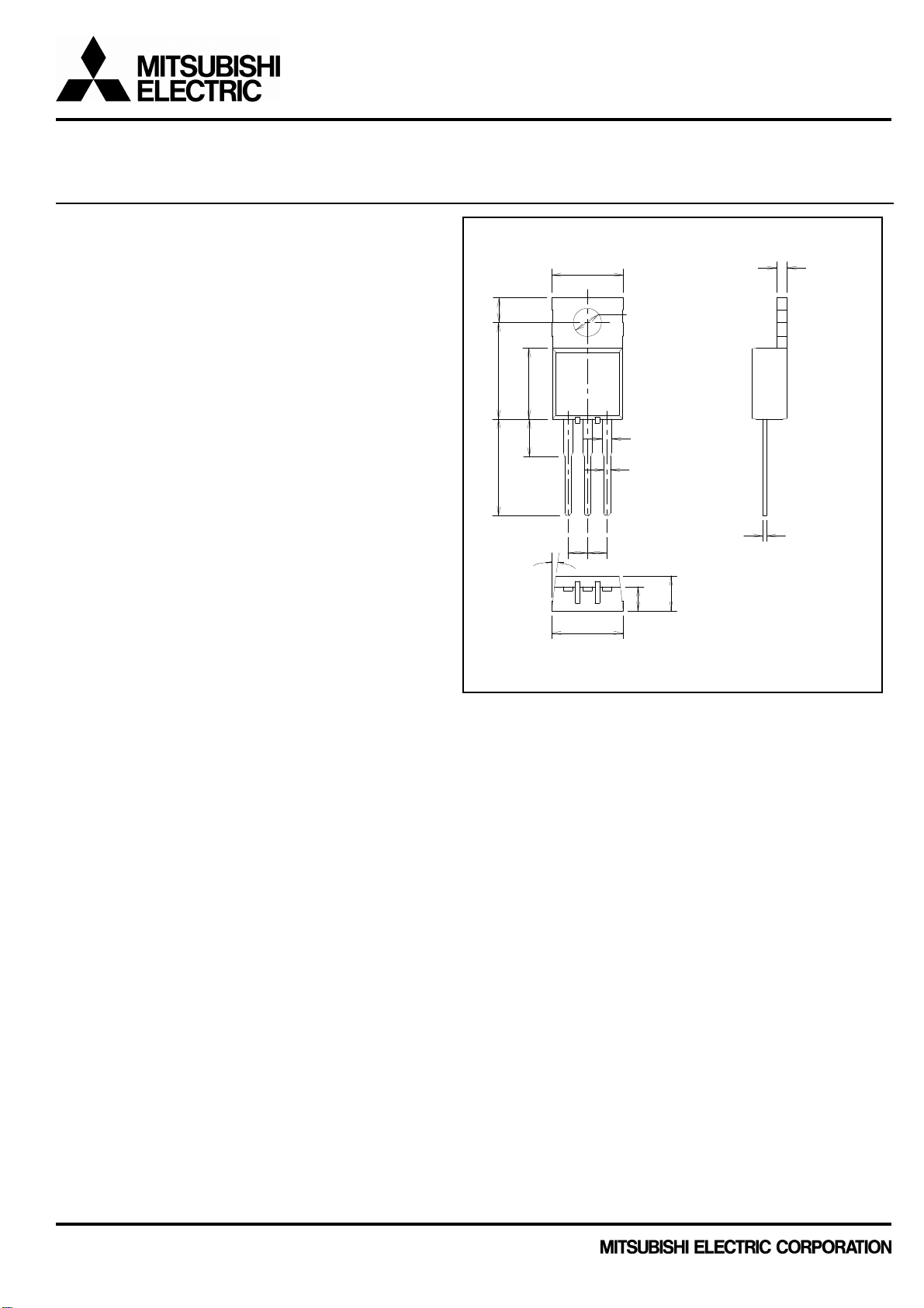
Dimension in mm.
RD15HVF1
RoHS Compliance, Silicon MOSFET Power Transistor, 175MHz520MHz,15W
DESCRIPTION
RD15HVF1 is a MOS FET type transistor specifically
designed for VHF/UHF High power amplifiers applica
-tions.
FEATURES
High power and High Gain:
Pout>15W, Gp>14dB @Vdd=12.5V,f=175MHz
Pout>15W, Gp>7dB @Vdd=12.5V,f=520MHz
High Efficiency: 60%typ. on VHF Band
High Efficiency: 55%typ. on UHF Band
APPLICATION
For output stage of high power amplifiers in VHF/UHF
Band mobile radio sets.
OUTLINE DRAWING
9.1+/-0.7
.4
3.2+/-0
1
2.5
2
2.5
9.5MAX
2
1.2+/-0.4
0.8+0.10/-0.15
3
0.6
12.3+/-
+/-0.4
9
N
4.8MAX
12.3MI
5deg
note:
Torelance of no designation means typical value.
3.6+/-0.2
.1+/-0.6
3
1.3+/-0.4
0.5+0.10/-0.15
.5
4.5+/-0
PINS
1:GATE
2:SOURCE
3:DRAIN
RoHS COMPLIANT
RD15HVF1-101 is a RoHS compliant products.
RoHS compliance is indicate by the letter “G” after the lot
marking.
This product include the lead in high melting temperature type solders.
However, it is applicable to the following exceptions of RoHS Directions.
1.Lead in high melting temperature type solders(i.e.tin-lead solder alloys containing more than85% lead.)
Publication Date : Oct.2011
1

< Silicon RF Power MOS FET (Discrete) >
RD15HVF1
RoHS Compliance, Silicon MOSFET Power Transistor, 175MHz520MHz,15W
ABSOLUTE MAXIMUM RATINGS
(Tc=25°CUNLESS OTHERWISE NOTED)
SYMBOL PARAMETER CONDITIONS RATINGS UNIT
V
DSS
V
GSS
Pch Channel dissipation Tc=25
Pin Input power Zg=Zl=50
ID Drain current - 4
Tch Channel temperature - 150
Tstg Storage temperature - -40 to +150
Rth j-c Thermal resistance junction to case 2.6
Note 1: Above parameters are guaranteed independently.
Note 2: Over 300MHz use spec is 6W
Drain to source voltage Vgs=0V 30 V
Gate to source voltage Vds=0V +/-20 V
°C
48 W
1.5(Note2)
ELECTRICAL CHARACTERISTICS (Tc=25°C , UNLESS OTHERWISE NOTED)
SYMBOL PARAMETER CONDITIONS
LIMITS UNIT
MIN TYP MAX.
W
A
°C
°C
°C/W
I
DSS
I
GSS
V
Pout1 Output power VDD=12.5V, Pin=0.6W, 15 18 - W
D1
Pout2 Output power VDD=12.5V, Pin=3W, 15 18 - W
D2
Note : Above parameters , ratings , limits and conditions are subject to change.
Zero gate voltage drain current VDS=17V, VGS=0V - - 100 uA
Gate to source leak current VGS=10V, VDS=0V - - 1 uA
Gate threshold Voltage VDS=12V, IDS=1mA 1.5 2.0 2.5 V
TH
Drain efficiency f=175MHz,Idq=0.5A 55 60 - %
Drain efficiency f=520MHz,Idq=0.5A 50 55 - %
Load VSWR tolerance VDD=15.2V,Po=15W(PinControl)
f=175MHz,Idq=0.5A,Zg=50
Load VSWR=20:1(All Phase)
Load VSWR tolerance VDD=15.2V,Po=15W(PinControl)
f=520MHz,Idq=0.5A,Zg=50
Load VSWR=20:1(All Phase)
No destroy -
No destroy -
Publication Date : Oct.2011
2
< Silicon RF Power MOS FET (Discrete) >
RD15HVF1
RoHS Compliance, Silicon MOSFET Power Transistor, 175MHz520MHz,15W
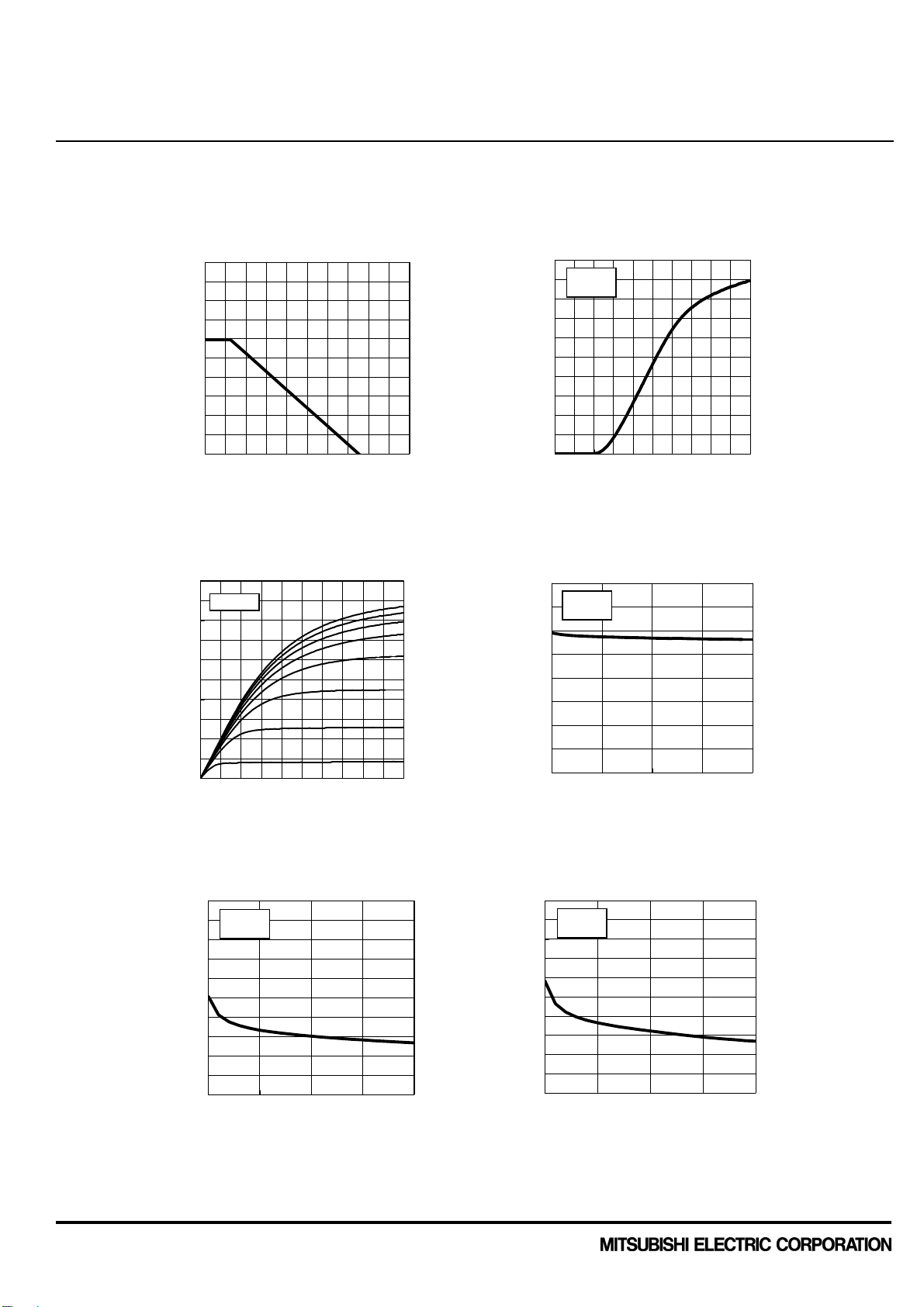
TYPICAL CHARACTERISTICS
CHANNNEL DISSIPATION VS.
AMBIENT TEMPERATURE
100
80
60
40
Pch(W)
20
CHANNEL DISSIPATION
0
0 40 80 120 160 200
AMBIENT TEMPERATURE Ta(°C)
Vds-Ids CHARACTERISTICS
10
Ta=+25°C
8
6
Ids(A)
4
2
0
0 2 4 6 8 10
Vds(V)
Vgs=10V
Vgs=9V
Vgs=8V
Vgs=7V
Vgs=6V
Vgs=5V
Vgs=4V
Vgs=3V
Vgs-Ids CHARACTERISTICS
10
Ta=+25°C
Vds=10V
8
6
Ids(A)
4
2
0
0 2 4 6 8 10
Vgs(V)
Vds VS. Ciss CHARACTERISTICS
80
Ta=+25°C
f=1MHz
60
40
Ciss(pF)
20
0
0 5 10 15 20
Vds(V)
Vds VS. Coss CHARACTERISTICS
100
Ta=+25°C
f=1MHz
80
60
40
Coss(pF)
20
0
0 5 10 15 20
Publication Date : Oct.2011
Vds(V)
Vds VS. Crss CHARACTERISTICS
10
Ta=+25°C
f=1MHz
8
6
4
Crss(pF)
2
0
0 5 10 15 20
Vds(V)
3
 Loading...