

Page 1
< Silicon RF Power MOS FET (Discrete) >
RD09MUP2
RoHS Compliance, Silicon MOSFET Power Transistor, 520MHz, 8W
DESCRIPTION
RD09MUP2 is a MOS FET type transistor
specifically designed for UHF RF power
amplifiers applications.
FEATURES
•High power gain:
Pout>8W, Gp>10dB@Vdd=7.2V,f=520MHz
•High Efficiency: 50%min. (520MHz)
•Integrated gate protection diode
APPLICATION
For output stage of high power amplifiers in
UHF band mobile radio sets.
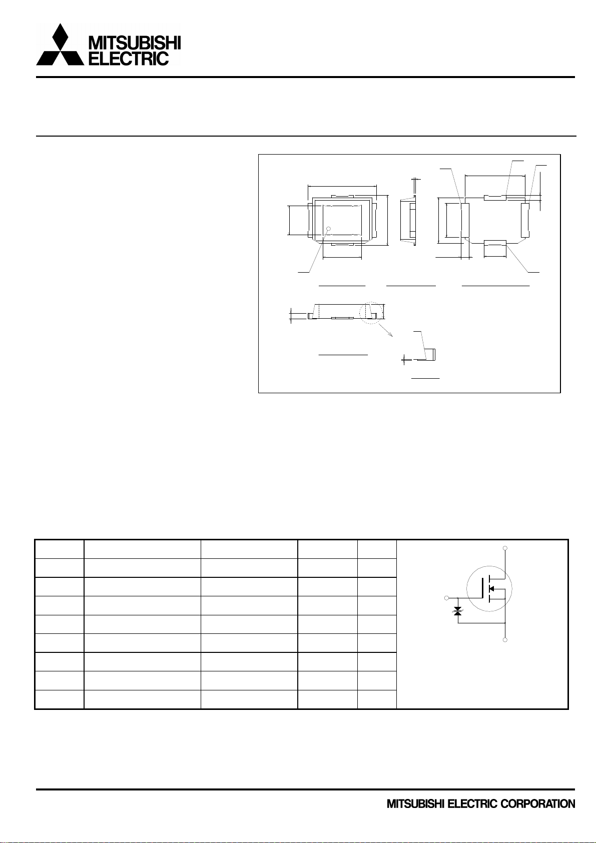
INDEX MARK
[Gate]
(b)
8.0+/-0 .2
(3.6)
(d)
(4.5)
0.2+/-0 .05
6.2+/-0.2
4.2+/-0.2
5.6+/-0.2
0.95+/- 0.2
TOP VIEW SIDE VIEW BOTTOM VIEW
DETAI L A
0.7+/-0.1
1.8+/-0.1
SIDE VIEW
DETA IL A
Standoff = max 0.05
7.0+/-0 .2
2.6+/-0 .2
Term inal N o.
(a)Dr ain [ou tput]
(b)So urce [GND ]
(c)Ga te [in put]
(d)So urce
UNIT: mm
NOTE S:
1. ( ) Typic al va lue
RoHS COMPLIANT
RD09MUP2 is a RoHS compliant product. RoHS compliance is indicating by the letter “G” after the Lot Marking.
This product includes the lead in high melting temperature type solders.
However, it is applicable to the following exceptions of RoHS Directions.
1.Lead in high melting temperature type solders (i.e. tin-lead older alloys containing more than85% lead.)
(a)
(b)
0.65+/-0.2
(c)
ABSOLUTE MAXIMUM RATINGS (Tc=25°C UNLESS OTHERWISE NOTED)
SYMBOL PARAMETER CONDITIONS RATINGS UNIT
VDSS Drain to source voltage Vgs=0V 40 V
VGSS Gate to source voltage Vds=0V -5 to +10 V
ID Drain Current - 4.0 A
Pin Input Power Zg=Zl=50
Pch Channel dissipation Tc=25
°C
Tj Junction Temperature - 150
Tstg Storage temperature - -40 to +125
Rth j-c Thermal resistance Junction to case 1.5
Note: Above parameters are guaranteed independently.
1.6 W
83 W
°C
°C
°C/W
Publication Date : Oct.2011
1
G
SCHEMATIC DRAWING
D
S
Page 2
< Silicon RF Power MOS FET (Discrete) >
RD09MUP2
RoHS Compliance, Silicon MOSFET Power Transistor, 520MHz, 8W
ELECTRICAL CHARACTERISTICS
SYMBOL PARAMETER CONDITIONS
I
DSS
I
GSS
V
TH
Pout Output power 8 9 - W
D
VSWRT Load VSWR tolerance
Note: Above parameters, ratings, limits and conditions are subject to change.
Zero gate voltage drain current VDS=17V, VGS=0V - - 10 uA
Gate to source leak current VGS=10V, VDS=0V - - 1 uA
Gate threshold Voltage VDS=12V, IDS=1mA 0.5 - 2.5 V
Drain efficiency
(Tc=25°C, UNLESS OTHERWISE NOTED)
LIMITS UNIT
MIN TYP MAX.
f=520MHz , VDD=7.2V
Pin=0.8W,Idq=1.0A
VDD=9.5V,Po=8W(Pin Control)
f=520MHz,Idq=1.0A,Zg=50
Load VSWR=20:1(All Phase)
50 - - %
No destroy -
Publication Date : Oct.2011
2
Page 3
< Silicon RF Power MOS FET (Discrete) >
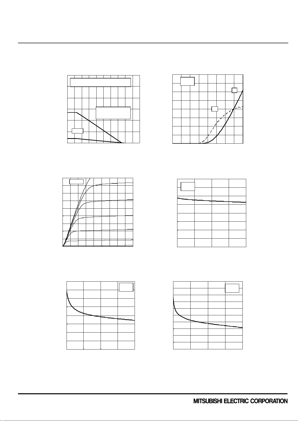
CHANNEL DISSIPATION Pch(W)
Coss(pF)
RD09MUP2
RoHS Compliance, Silicon MOSFET Power Transistor, 520MHz, 8W
TYPICAL CHARACTERISTICS
CHANNEL DISSIPATION VS.
60
,,,
50
AMBIENT TEMPERATURE
*PCB: Glass epoxy (Size : 46.4 x40.0mm, t=0.8mm)
Thermal sheet: GELTEC COOH-4000(t=0.5mm)
40
30
20
10
Free Air
On PCB withTermal sheet
andHeat-sink
(Size : 41 x55mm, t=7.2 mm)
0
0 40 80 120 160 200
AMBIENT TEMPERATURE Ta(deg:C.)
Vds-Ids CHARACTERISTICS
9
Ta=+25°C
8
7
6
5
4
Ids(A)
3
2
1
0
0 1 2 3 4 5 6 7 8 9
Vds( V)
Vgs=4.5V
Vgs=4.0V
Vgs=3.5V
Vgs=3.0V
Vgs-Ids CHARACTERISTICS
8
Ta=+25°C
Vds=10V
6
4
GM
Ids(A),GM(S)
2
0
0 1 2 3 4
Vgs(V)
Vds VS. Ciss CHARACTERISTICS
160
Ta=+25°C
140
f=1MHz
120
100
80
Ciss(pF)
60
40
20
0
0 5 10 15 20
Vds(V)
Ids
Publication Date : Oct.2011
Vds V S. Cos s CHARACTERISTICS
160
140
120
100
80
60
40
20
0
0 5 10 15 20
Vds(V)
Ta=+25°C
f=1MHz
Vds VS. Crss CHARACTERISTICS
20
18
Ta=+25°C
f=1MHz
16
14
12
10
Crss (pF)
8
6
4
2
0
0 5 10 15 20
Vds(V)
3
Page 4

< Silicon RF Power MOS FET (Discrete) >
Po(dBm) , Gp(dB) , Idd(A)
RD09MUP2
RoHS Compliance, Silicon MOSFET Power Transistor, 520MHz, 8W
TYPICAL CHARACTERISTICS
Pin-Po CHARACTERISTICS @f=520MHz
Ta=+25°C
40
f=520MHz
Vdd=7.2V
Idq=1.0A
Po
30
20
Gp
10
Idd
0
0 5 10 15 20 25 30 35
Pin(dBm)
Vdd-Po CHARACTERISTICS @f=520MHz
20
Ta=25°C
f=520MHz
Pin=1.0W
15
Idq=1.0A
Zg= ZI=50 ohm
Po
Pin-Po CHARACTERISTICS @f=520MHz
20
15
Ta=25°C
f=520MHz
Vdd=7.2V
Idq=1.0A
ηd
80
60
Po
η
d
40
ηd(%)
10
80
70
60
50
40
ηd(%)
30
Pout(W) , Idd(A)
20
5
Idd
20
10
0
0
0
0.0 0.5 1.0 1.5 2.0
Pin(W)
10
8
10
Po(W)
5
0
4 6 8 10 12
Vdd(V)
5
Idd(A)
Idd
3
0
Publication Date : Oct.2011
4
Page 5

< Silicon RF Power MOS FET (Discrete) >
RD09MUP2
RoHS Compliance, Silicon MOSFET Power Transistor, 520MHz, 8W
TEST CIRCUIT (f=520MHz)
C1
19mm
W W
4.7k OHM
330pF
RF-in
Note:Boad material Glass-Epoxy Substrate
Micro strip line width=1.3mm/50 OHM、er:4.8、t=0.8mm
W:Line width=1.0mm
13mm
5pF
3mm
3.5mm
Vgg
33pF
6mm
RD09MUP2
520MHz
22μF、50V
C2
L
3mm 7mm
L:24.9nH、6Turns、D:0.43mm、φ2.46mm(outside diameter)
C1、C2:2200pF
5mm
47pF
Vdd
19mm
21mm
5pF
RF-OUT
330pF
5pF
Publication Date : Oct.2011
5
Page 6

< Silicon RF Power MOS FET (Discrete) >
RD09MUP2 S-PARAMETER DATA (@Vdd=7.2V, Id=500mA)
Freq.
[MHz]
(mag)
(ang)
(mag)
(ang)
(mag)
(ang)
(mag)
(ang)
100
0.900
-175.7
4.425
75.0
0.016
-7.1
0.798
-173.9
120
0.901
-176.4
3.651
71.1
0.014
-8.2
0.804
-174.4
140
0.905
-176.7
3.056
67.4
0.014
-10.4
0.808
-174.9
160
0.908
-177.2
2.614
64.2
0.013
-10.9
0.812
-175.1
180
0.909
-177.5
2.273
61.4
0.013
-10.0
0.819
-175.2
200
0.912
-177.6
2.003
58.7
0.011
-8.4
0.830
-175.1
220
0.916
-178.0
1.787
55.9
0.011
-6.0
0.842
-175.3
240
0.918
-178.5
1.602
53.3
0.010
-4.1
0.851
-175.3
260
0.922
-178.7
1.442
50.6
0.010
-5.6
0.857
-175.8
280
0.923
-178.9
1.297
48.0
0.009
0.6
0.859
-176.1
300
0.928
-179.0
1.176
45.8
0.008
2.6
0.863
-176.3
320
0.930
-179.1
1.075
44.1
0.008
8.2
0.866
-176.8
340
0.933
-179.3
0.989
42.3
0.008
15.1
0.878
-177.1
360
0.936
-179.6
0.910
40.0
0.008
25.3
0.889
-177.4
380
0.937
179.9
0.841
37.9
0.007
27.2
0.895
-177.8
400
0.939
179.7
0.775
36.3
0.008
35.5
0.897
-178.1
420
0.939
179.3
0.718
34.7
0.008
40.1
0.899
-178.6
440
0.945
179.1
0.667
33.4
0.008
45.0
0.900
-178.8
460
0.947
178.9
0.622
32.1
0.009
51.3
0.906
-179.3
480
0.950
178.8
0.582
30.7
0.009
56.2
0.913
-179.5
500
0.952
178.7
0.548
29.2
0.010
56.9
0.919
179.8
520
0.950
178.3
0.513
28.0
0.011
59.9
0.921
179.6
540
0.952
178.1
0.480
26.8
0.012
64.2
0.924
179.0
560
0.953
177.6
0.455
25.7
0.012
67.0
0.925
178.8
580
0.953
177.2
0.427
24.4
0.012
66.6
0.924
178.6
600
0.956
177.0
0.402
23.7
0.014
68.9
0.928
178.2
620
0.957
177.0
0.383
23.2
0.014
70.7
0.933
177.7
640
0.961
176.9
0.362
22.1
0.015
70.9
0.937
177.3
660
0.957
176.8
0.344
21.3
0.015
72.1
0.939
177.0
680
0.961
176.5
0.326
20.4
0.016
72.0
0.936
176.7
700
0.962
176.2
0.311
19.5
0.017
74.3
0.937
176.4
720
0.960
176.0
0.298
19.0
0.018
74.2
0.937
176.1
740
0.962
175.5
0.283
18.6
0.019
74.5
0.938
175.8
760
0.963
175.3
0.269
17.5
0.019
74.9
0.943
175.5
780
0.963
175.2
0.259
17.2
0.020
74.1
0.944
175.0
800
0.964
175.0
0.247
16.9
0.021
72.8
0.949
174.7
820
0.962
175.0
0.237
16.5
0.022
75.4
0.946
174.7
840
0.964
174.7
0.230
15.8
0.022
75.1
0.946
174.5
860
0.965
174.5
0.220
16.2
0.023
76.0
0.944
174.1
880
0.965
174.1
0.211
15.4
0.024
75.8
0.948
173.8
900
0.962
173.8
0.202
15.1
0.025
75.0
0.949
173.4
920
0.967
173.5
0.193
15.0
0.026
75.8
0.952
172.8
940
0.963
173.5
0.189
14.4
0.026
75.8
0.952
172.7
960
0.964
173.2
0.180
13.8
0.027
75.6
0.949
172.7
980
0.966
173.1
0.176
14.6
0.028
76.0
0.951
172.6
1000
0.964
173.0
0.170
14.0
0.029
76.5
0.952
172.2
RD09MUP2
RoHS Compliance, Silicon MOSFET Power Transistor, 520MHz, 8W
S11 S21 S12 S22
Publication Date : Oct.2011
6
Page 7

< Silicon RF Power MOS FET (Discrete) >
RD09MUP2 S-PARAMETER DATA (@Vdd=7.2V, Id=900mA)
Freq.
[MHz]
(mag)
(ang)
(mag)
(ang)
(mag)
(ang)
(mag)
(ang)
100
0.914
-176.9
4.363
78.5
0.012
0.2
0.825
-175.5
120
0.918
-177.4
3.638
74.9
0.012
-0.6
0.833
-176.2
140
0.920
-178.0
3.060
71.4
0.011
0.3
0.832
-177.1
160
0.922
-178.3
2.614
68.8
0.011
1.6
0.829
-177.3
180
0.921
-178.6
2.287
66.7
0.011
4.4
0.833
-177.4
200
0.921
-178.8
2.039
64.6
0.010
6.5
0.846
-177.2
220
0.922
-179.3
1.840
62.1
0.010
8.5
0.863
-177.4
240
0.925
-179.4
1.665
59.6
0.010
8.0
0.870
-177.5
260
0.924
-179.8
1.503
56.8
0.009
10.9
0.868
-177.9
280
0.928
180.0
1.364
54.7
0.009
13.1
0.864
-178.2
300
0.929
-180.0
1.240
52.9
0.009
18.6
0.860
-178.1
320
0.936
180.0
1.144
51.1
0.009
26.6
0.866
-178.4
340
0.935
179.8
1.064
49.4
0.009
27.8
0.879
-178.8
360
0.936
179.4
0.993
47.2
0.009
32.4
0.891
-179.0
380
0.937
179.0
0.923
45.2
0.009
34.4
0.896
-179.4
400
0.937
178.9
0.851
43.5
0.009
40.1
0.896
-179.7
420
0.939
178.5
0.795
41.7
0.009
47.0
0.895
-179.8
440
0.941
178.5
0.738
40.4
0.009
52.8
0.892
-180.0
460
0.944
178.3
0.696
39.3
0.010
50.3
0.898
179.6
480
0.946
178.1
0.654
38.0
0.011
56.9
0.908
179.3
500
0.948
178.0
0.619
36.5
0.011
59.5
0.912
178.8
520
0.950
177.9
0.585
34.8
0.012
62.7
0.914
178.4
540
0.949
177.5
0.549
33.5
0.012
63.1
0.915
178.1
560
0.948
177.1
0.518
32.2
0.014
63.6
0.916
178.0
580
0.950
177.0
0.491
31.1
0.014
65.6
0.918
177.8
600
0.952
176.6
0.467
30.3
0.014
66.3
0.919
177.6
620
0.954
176.5
0.444
29.5
0.015
67.6
0.924
177.0
640
0.958
176.5
0.426
28.5
0.016
69.8
0.930
176.4
660
0.954
176.4
0.400
27.2
0.017
69.8
0.932
176.3
680
0.957
176.3
0.382
26.3
0.017
70.8
0.929
176.0
700
0.956
176.0
0.367
25.6
0.018
71.9
0.929
175.9
720
0.955
175.5
0.350
24.9
0.019
72.4
0.931
175.8
740
0.956
175.2
0.334
23.9
0.019
72.5
0.930
175.3
760
0.959
174.9
0.319
23.4
0.020
73.0
0.934
174.8
780
0.958
175.0
0.308
22.3
0.021
72.7
0.939
174.5
800
0.959
174.8
0.293
22.0
0.021
74.0
0.944
174.3
820
0.962
174.8
0.281
21.5
0.022
73.9
0.939
174.1
840
0.962
174.5
0.271
21.0
0.023
74.2
0.938
174.0
860
0.961
174.3
0.261
20.4
0.023
74.1
0.939
173.9
880
0.960
174.0
0.252
20.0
0.025
73.9
0.940
173.4
900
0.961
173.6
0.244
19.5
0.025
74.6
0.942
173.0
920
0.961
173.3
0.233
18.9
0.026
74.4
0.944
172.5
940
0.960
173.3
0.225
18.5
0.027
74.7
0.945
172.3
960
0.962
173.1
0.219
18.2
0.027
74.7
0.945
172.3
980
0.962
172.9
0.211
17.5
0.029
74.3
0.948
172.4
1000
0.960
172.8
0.206
18.0
0.029
74.4
0.948
172.0
RD09MUP2
RoHS Compliance, Silicon MOSFET Power Transistor, 520MHz, 8W
S11 S21 S12 S22
Publication Date : Oct.2011
7
Page 8

< Silicon RF Power MOS FET (Discrete) >
have
until cold after switch
his products without cause damage for human and
details
copies of the formal
(RF power transistors) are designed
other applications.
In particular, while these products are highly reliable for their designed purpose, they are not manufactured
quality assurance testing protocol that is sufficient to guarantee the level of reliability typically deemed
In the application, which is base station applications and
off frequency
during transmitting, please consider the derating, the redundancy system, appropriate setting of the maintain
predicted operating life time of
an authorized Mitsubishi
therefore
device is
It is
sink in conjunction with other cooling methods as needed (fan,
lower than 120deg/C(in case of
6. Do not use the device at the exceeded the maximum rating condition. In case of plastic molded devices, the
exceeded maximum rating condition may cause blowout, smoldering or catch fire of the molding resin due to
extreme short current flow between the drain and the source of the device. These results causes in fire or
the
Warranty for the product is void if the products protective cap (lid) is removed or if the product is modified in
, please refer the last page
RD09MUP2
RoHS Compliance, Silicon MOSFET Power Transistor, 520MHz, 8W
ATTENTION:
1.High Temperature ; This product might have a heat generation while operation,Please take notice that
a possibility to receive a burn to touch the operating product directly or touch the product
off. At the near the product,do not place the combustible material that have possibilities to arise the fire.
2.Generation of High Frequency Power ; This product generate a high frequency power. Please take notice
that do not leakage the unnecessary electric wave and use t
property per normal operation.
3.Before use; Before use the product,Please design the equipment in consideration of the risk for human and
electric wave obstacle for equipment.
PRECAUTIONS FOR THE USE OF MITSUBISHI SILICON RF POWER DEVICES:
1. The specifications of mention are not guarantee values in this data sheet. Please confirm additional
regarding operation of these products from the formal specification sheet. For
specification sheets, please contact one of our sales offices.
2.RA series products (RF power amplifier modules) and RD series products
for consumer mobile communication terminals and were not specifically designed for use in
under a
necessary for critical communications elements and
fixed station applications that operate with long term continuous transmission and a higher on-
period and others as needed. For the reliability report which is described about
Mitsubishi Silicon RF Products , please contact Mitsubishi Electric Corporation or
Semiconductor product distributor.
3. RD series products use MOSFET semiconductor technology. They are sensitive to ESD voltage
appropriate ESD precautions are required.
4. In the case of use in below than recommended frequency, there is possibility to occur that the
deteriorated or destroyed due to the RF-swing exceed the breakdown voltage.
5. In order to maximize reliability of the equipment, it is better to keep the devices temperature low.
recommended to utilize a sufficient sized heatetc.) to keep the channel temperature for RD series products
Tchmax=150deg/C) ,140deg/C(in case of Tchmax=175deg/C) under standard conditions.
injury.
7. For specific precautions regarding assembly of these products into the equipment, please refer to
supplementary items in the specification sheet.
8.
any way from it’s original form.
9. For additional “Safety first” in your circuit design and notes regarding the materials
of this data sheet.
10. Please refer to the additional precautions in the formal specification sheet.
Publication Date : Oct.2011
8
Page 9

< Silicon RF Power MOS FET (Discrete) >
RD09MUP2
RoHS Compliance, Silicon MOSFET Power Transistor, 520MHz, 8W
Keep safety first in your circuit designs!
Mitsubishi Electric Corporation puts the maximum effort into making semiconductor products better and more
reliable, but there is always the possibility that trouble may occur with them. Trouble with semiconductors may lead
to personal injury, fire or property damage. Remember to give due consideration to safety when making your circuit
designs, with appropriate measures such as (i) placement of substitutive, auxiliary circuits, (ii) use of
non-flammable material or (iii) prevention against any malfunction or mishap.
Notes regarding these materials
•These materials are intended as a reference to assist our customers in the selection of the Mitsubishi
semiconductor product best suited to the customer’s application; they do not convey any license under any
intellectual property rights, or any other rights, belonging to Mitsubishi Electric Corporation or a third party.
•Mitsubishi Electric Corporation assumes no responsibility for any damage, or infringement of any third-party’s
rights, originating in the use of any product data, diagrams, charts, programs, algorithms, or circuit application
examples contained in these materials.
•All information contained in these materials, including product data, diagrams, charts, programs and algorithms
represents information on products at the time of publication of these materials, and are subject to change by
Mitsubishi Electric Corporation without notice due to product improvements or other reasons. It is therefore
recommended that customers contact Mitsubishi Electric Corporation or an authorized Mitsubishi Semiconductor
product distributor for the latest product information before purchasing a product listed herein.
The information described here may contain technical inaccuracies or typographical errors. Mitsubishi Electric
Corporation assumes no responsibility for any damage, liability, or other loss rising from these inaccuracies or
errors.
Please also pay attention to information published by Mitsubishi Electric Corporation by various means, including
the Mitsubishi Semiconductor home page (http://www.MitsubishiElectric.com/).
•When using any or all of the information contained in these materials, including product data, diagrams, charts,
programs, and algorithms, please be sure to evaluate all information as a total system before making a final
decision on the applicability of the information and products. Mitsubishi Electric Corporation assumes no
responsibility for any damage, liability or other loss resulting from the information contained herein.
•Mitsubishi Electric Corporation semiconductors are not designed or manufactured for use in a device or system
that is used under circumstances in which human life is potentially at stake. Please contact Mitsubishi Electric
Corporation or an authorized Mitsubishi Semiconductor product distributor when considering the use of a product
contained herein for any specific purposes, such as apparatus or systems for transportation, vehicular, medical,
aerospace, nuclear, or undersea repeater use.
•The prior written approval of Mitsubishi Electric Corporation is necessary to reprint or reproduce in whole or in part
these materials.
•If these products or technologies are subject to the Japanese export control restrictions, they must be exported
under a license from the Japanese government and cannot be imported into a country other than the approved
destination.
Any diversion or re-export contrary to the export control laws and regulations of Japan and/or the country of
destination is prohibited.
•Please contact Mitsubishi Electric Corporation or an authorized Mitsubishi Semiconductor product distributor for
further details on these materials or the products contained therein.
© 2011 MITSUBISHI ELECTRIC CORPORATION. ALL RIGHTS RESERVED.
Publication Date : Oct.2011
9
 Loading...