

Page 1
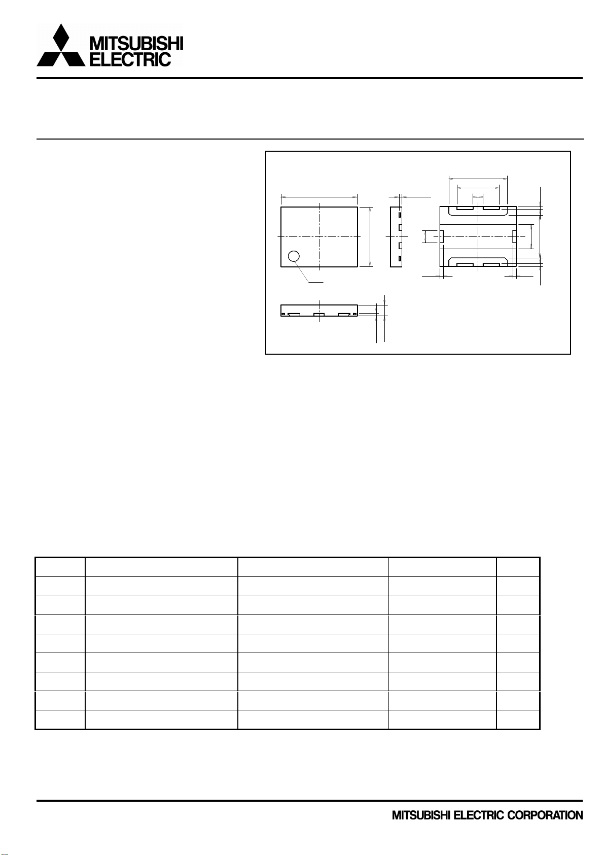
UNIT:mm
< Silicon RF Power MOS FET (Discrete) >
RD07MUS2B
RoHS Compliance, Silicon MOSFET Power Transistor,175MHz,527MHz,870MHz,7W
OUTLINE DRAWING
DESCRIPTION
RD07MUS2B is a MOS FET type transistor
specifically designed for VHF/UHF/870MHz
RF power amplifiers applications.
FEATURES
High power gain and High Efficiency.
Typical Po Gp ηD
(175MHz) 7.2W 13.8dB 65%
(527MHz) 8W 13.0dB 63%
(870MHz) 7W 11.5dB 58%
Integrated gate protection diode.
APPLICATION
For output stage of high power amplifiers in
VHF/UHF/800MHz-band mobile radio sets.
6.0+/-0.15
INDEX MARK
4.9+/-0.15
(Gate)
0.2+/-0.05
0.2+/-0.05
1.0+/-0.05
(0.25)
0.9+/-0.1
4.6+/-0.05
3.3+/-0.05
0.8+/-0.05
1
2
3
Terminal No.
1.Drain (output)
2.Source (GND)
3.Gate (input)
Note
( ):center value
(0.25)
2.0+/-0.05
3.5+/-0.05
(0.22) (0.22)
RoHS COMPLIANT
RD07MUS2B is a RoHS compliant product. RoHS compliance is indicating by the letter “G” after the Lot Marking.
This product includes the lead in high melting temperature type solders.
However, it is applicable to the following exceptions of RoHS Directions.
1. Lead in high melting temperature type solders(i.e.tin-lead solder alloys containing more than85% lead.)
ABSOLUTE MAXIMUM RATINGS (Tc=25°C UNLESS OTHERWISE NOTED)
SYMBOL PARAMETER CONDITIONS RATINGS UNIT
VDSS Drain to source voltage Vgs=0V 25 V
VGSS Gate to source voltage Vds=0V -5/+10 V
Pch Channel dissipation Tc=25
Pin Input Power Zg=Zl=50
°C
ID Drain Current - 3 A
Tch Junction Temperature - 150
Tstg Storage temperature - -40 to +125
50 W
0.8* W
°C
°C
Rth j-c Thermal resistance Junction to case 2.5
Note: Above parameters are guaranteed independently.
*: 175MHz spec. is 0.6W
Publication Date : Oct.2011
1
°C/W
Page 2
< Silicon RF Power MOS FET (Discrete) >
RD07MUS2B
RoHS Compliance, Silicon MOSFET Power Transistor,175MHz,527MHz,870MHz,7W
ELECTRICAL CHARACTERISTICS (Tc=25°C, UNLESS OTHERWISE NOTED)
SYMBOL PARAMETER CONDITIONS
MIN TYP MAX.
I
DSS
I
GSS
V
Pout1 Output power - 7.2* - W
D1
Pout2 Output power 7** 8** - W
D2
Pout3 Output power - 7*** - W
D3
VSWRT Load VSWR tolerance
Note: Above parameters, ratings, limits and conditions are subject to change.
* At 135-175MHz broad matching ** At 450-527MHz broad matching *** At 763-870MHz broad matching
Drain cutoff current VDS=17V, VGS=0V - - 10 uA
Gate cutoff current VGS=5V, VDS=0V - - 1 uA
Gate threshold Voltage VDS=7.2V, IDS=1mA 0.5 1 1.5 V
TH
f=175MHz,VDD=7.2V
Drain efficiency
Drain efficiency
Drain efficiency
Pin=0.3W,Idq=250mA
f=527MHz ,VDD=7.2V
Pin=0.4W,Idq=250mA
f=870MHz ,VDD=7.2V
Pin=0.5W,Idq=250mA
VDD=9.5V,Po=7W(Pin Control)
f=527MHz,Idq=250mA,Zg=50
Load VSWR=20:1(All Phase)
58** 63** - %
LIMITS UNIT
- 65* - %
- 58*** - %
No destroy -
Publication Date : Oct.2011
2
Page 3
< Silicon RF Power MOS FET (Discrete) >
Crss(pF)
Coss(pF)
V
RD07MUS2B
RoHS Compliance, Silicon MOSFET Power Transistor,175MHz,527MHz,870MHz,7W
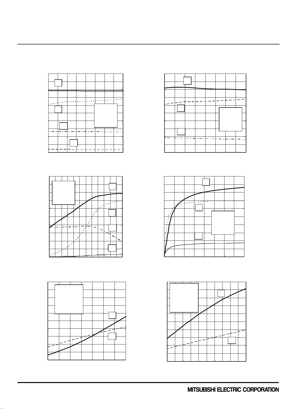
TYPICAL CHARACTERISTICS
(These are only typical curves and devices are not necessarily guaranteed at these curves.)
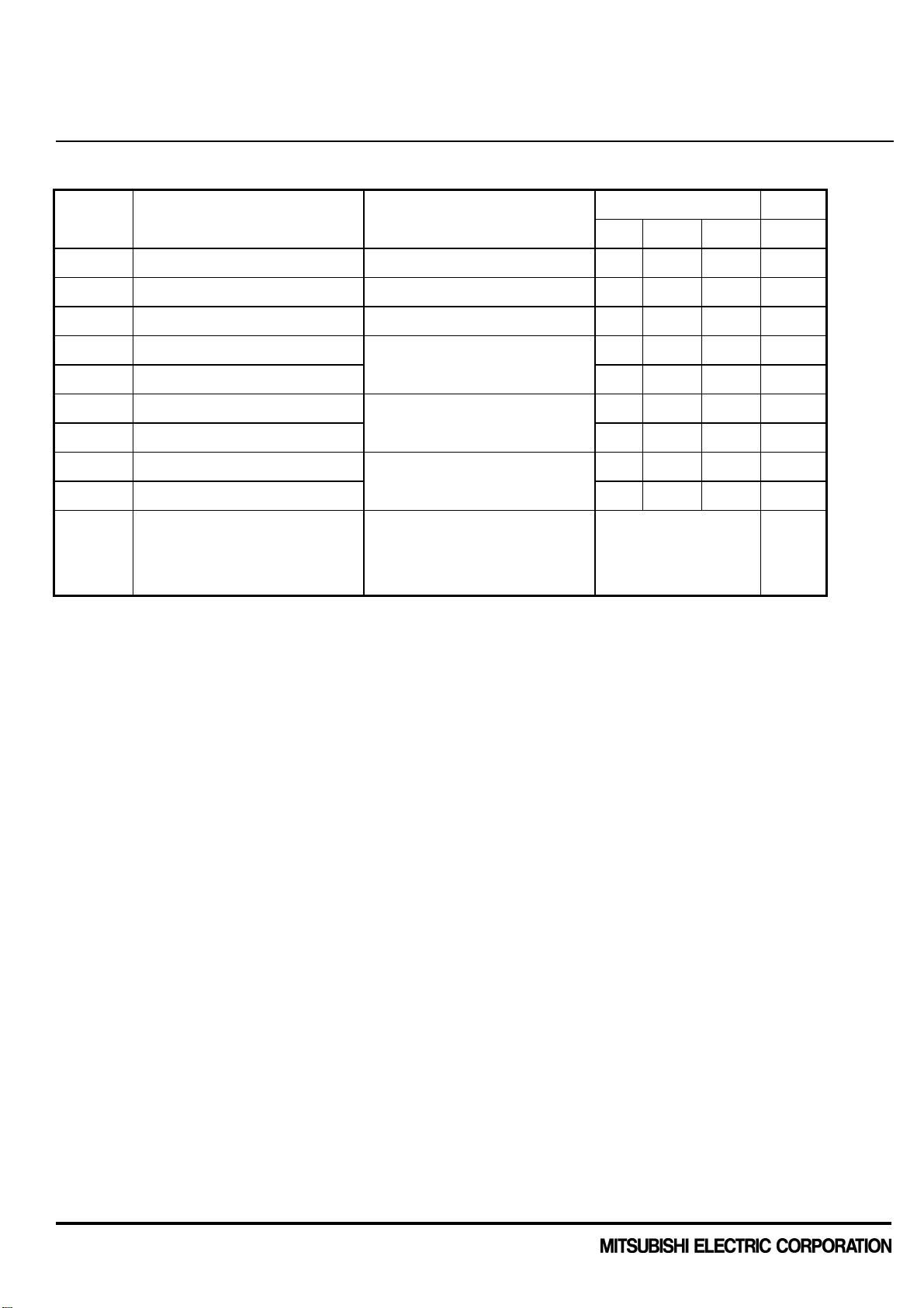
VDS-IDSCHARACTERISTICS
7
6
5
4
(A)
DS
I
3
2
1
0
0 2 4 6 8 10
160
140
120
100
80
60
Ciss(pF)
40
20
3V3.5V
Ta=+25°C
VGS=1.5V
VDS(V)
VDSVS. Ciss CHARACTERISTICS
Ta=+25°C
f=1MHz
2.5V
2V
7
6
5
(S)
4
m
(A),g
3
DS
I
2
1
0
120
100
VGS-IDSCHARACTERISTICS
Ta=+25°C
=10V
DS
g
m
I
DS
0 0.5 1 1.5 2 2.5 3
VDSVS. Cos s CHARACTERISTICS
Ta=+25°C
f=1MHz
80
60
40
20
VGS(V)
0
0 5 10 15 20
VDSVS. Crss CHARACTERISTICS
20
18
Ta=+25°C
f=1MHz
16
14
12
10
8
6
4
2
0
0 5 10 15 20
Publication Date : Oct.2011
VDS(V)
VDS(V)
0
0 5 10 15 20
VDS(V)
3
Page 4
< Silicon RF Power MOS FET (Discrete) >
Po(dBm) , Gp(dB) , Idd(A)
Po(dBm) , Gp(dB) , Idd(A)
RD07MUS2B
RoHS Compliance, Silicon MOSFET Power Transistor,175MHz,527MHz,870MHz,7W
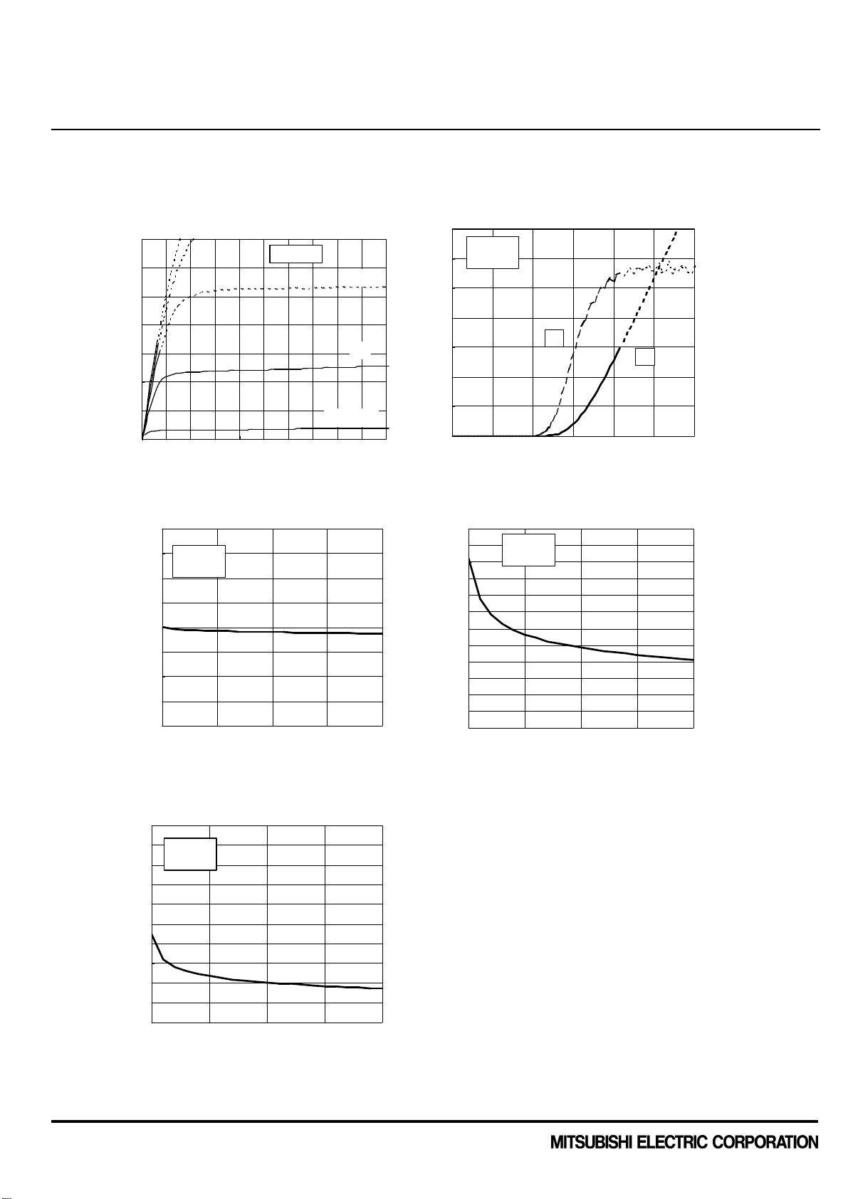
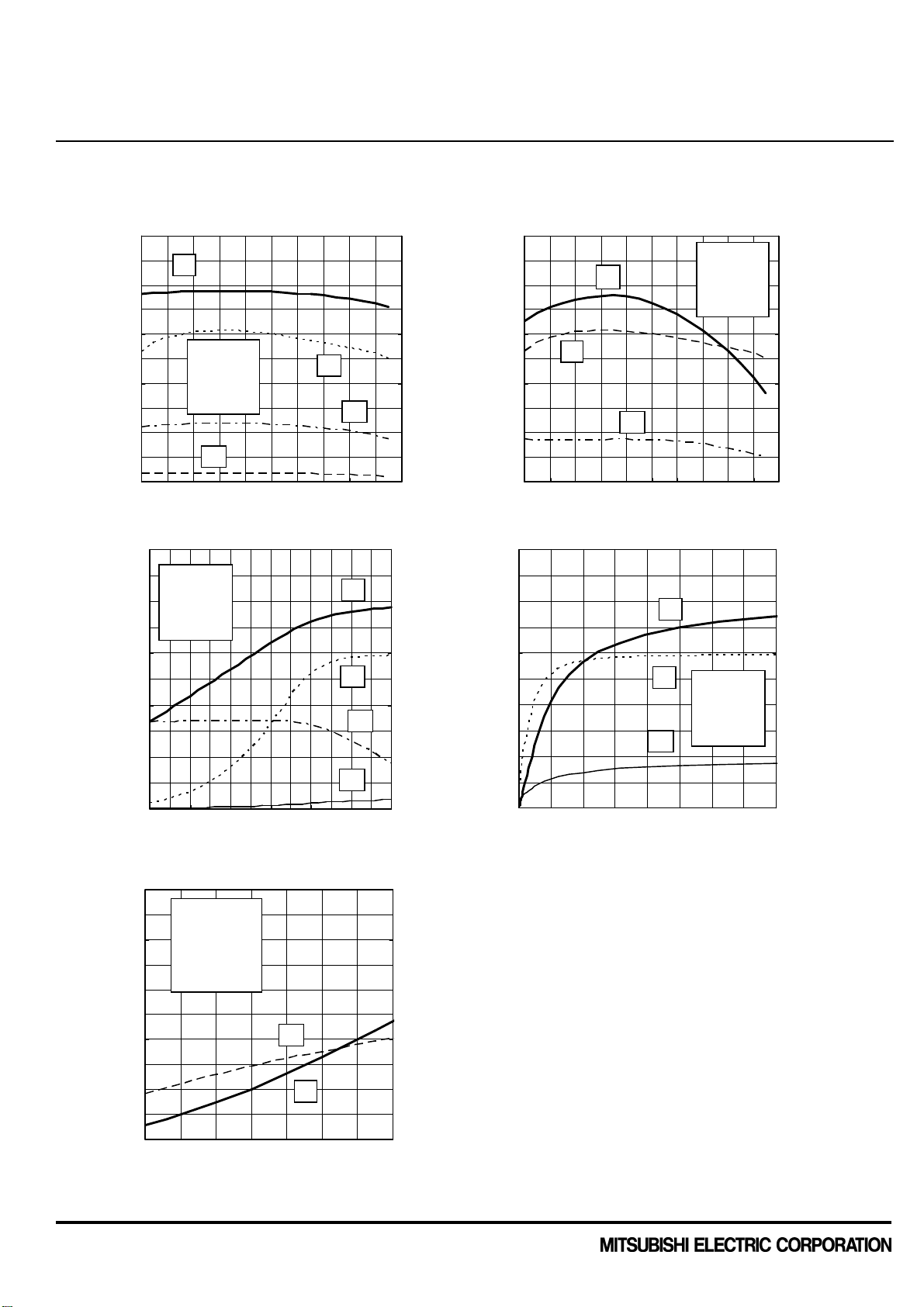
TYPICAL CHARACTERISTICS ( 135-175MHz )
(These are only typical curves and devices are not necessarily guaranteed at these curves.)
f-Po CHARACTERISTICS @f=135-175MHz
50
40
Po
100
80
f-Po CHARACTERISTICS @f=135-175MHz
10
Po
8
100
80
30
20
10
0
135 140 145 150 155 160 165 170 175
Pin-Po CHARACTERISTICS @f=175MHz
50
40
30
20
10
0
0 5 10 15 20 25 30
ηd
Gp
f (MHz)
Ta=+25°C
f=175MHz
Vdd=7.2V
Idq=250mA
Pin(dBm)
Ta=+25°C
Vdd=7.2V
Pin=0.3W
Idq=250mA
Idd
Po
ηd
Gp
Idd
60
40
20
0
100
80
60
40
20
0
6
ηd(%)
4
Pout(W) , Idd(A)
2
0
135 140 145 150 155 160 165 170 175
10
8
6
ηd(%)
4
Pout(W) , Idd(A)
2
0
0 0.2 0.4 0.6 0.8
ηd
Ta=+25°C
Vdd=7.2V
Pin=0.3W
Idd
f (MHz)
Pin-Po CHARACTERISTICS @f=175MHz
Idd
Pin(W)
Idq=250mA
Po
ηd
Ta=+25°C
f=175MHz
Vdd=7.2V
Idq=250mA
60
40
20
0
100
80
60
40
20
0
ηd(%)
ηd(%)
Vdd-Po CHARACTERISTICS @f=175MHz
25
20
15
Po(W)
10
5
0
3 4 5 6 7 8 9 10
Publication Date : Oct.2011
Ta=+25°C
f=175MHz
Pin=0.3W
Idq=250mA
Zg=ZI=50 ohm
Vdd(V )
Po
Idd
5
4
3
Idd(A)
2
1
0
Vgg-Po CHARACTERISTICS @f=175MHz
10
Ta=+25°C
f=175MHz
8
Pin=0.3W
Idq=250mA
Zg=ZI=50 ohm
6
Po(W)
4
2
0
0 0.4 0.8 1.2 1.6 2
Vgg(V )
Po
Idd
5
4
3
Idd(A)
2
1
0
4
Page 5
< Silicon RF Power MOS FET (Discrete) >
Po(dBm) , Gp(dB) , Idd(A)
Po(dBm) , Gp(dB) , Idd(A)
RD07MUS2B
RoHS Compliance, Silicon MOSFET Power Transistor,175MHz,527MHz,870MHz,7W
TYPICAL CHARACTERISTICS ( 450-527MHz )
(These are only typical curves and devices are not necessarily guaranteed at these curves.)
f-Po CHARACTERISTICS @f=450-527MHz
50
Po
40
30
20
10
ηd
Gp
Idd
0
450 460 470 480 490 500 510 520 530
f (MHz)
Pin-Po CHARACTERISTICS @f=527MHz
50
Ta=+25°C
f=527MHz
40
Vdd=7.2V
Idq=250mA
30
20
10
Ta=+25°C
Vdd=7.2V
Pin=0.4W
Idq=250mA
Po
ηd
Gp
Idd
100
80
60
40
20
0
100
80
60
40
20
f-Po CHARACTERISTICS @f=450-527MHz
10
Po
8
6
ηd(%)
ηd(%)
4
Pout(W) , Idd(A)
2
0
450 460 470 480 490 500 510 520 530
10
8
6
4
Pout(W) , Idd(A)
2
ηd
Idd
f (MHz)
Pin-Po CHARACTERISTICS @f=527MHz
Po
ηd
Idd
Ta=+25°C
Vdd=7.2V
Pin=0.4W
Idq=250mA
Ta=+25°C
f=527MHz
Vdd=7.2V
Idq=250mA
100
80
60
40
20
0
100
80
60
40
20
ηd(%)
ηd(%)
0
0 5 10 15 20 25 30
Vdd-Po CHARACTERISTICS @f=527MHz
25
Ta=+25°C
20
15
Po(W)
10
f=527MHz
Pin=0.4W
Idq=250mA
Zg=ZI=50 ohm
5
0
3 4 5 6 7 8 9 10
Publication Date : Oct.2011
Pin(dBm)
Vdd(V )
Po
Idd
0
5
4
3
Idd(A)
2
1
0
0
0.0 0.2 0.4 0.6 0.8
Pin(W)
Vgg-Po CHARACTERISTICS @f=527MHz
10
Ta=+25°C
f=527MHz
8
Pin=0.4W
Idq=250mA
Zg=ZI=50 ohm
6
Po(W)
4
2
0
0 0.4 0.8 1.2 1.6 2
Vgg(V )
Po
Idd
0
5
4
3
Idd(A)
2
1
0
5
Page 6
< Silicon RF Power MOS FET (Discrete) >
Po(dBm) , Gp(dB) , Idd(A)
Po(dBm) , Gp(dB) , Idd(A)
RD07MUS2B
RoHS Compliance, Silicon MOSFET Power Transistor,175MHz,527MHz,870MHz,7W
TYPICAL CHARACTERISTICS ( 763-870MHz )
(These are only typical curves and devices are not necessarily guaranteed at these curves.)
f-Po CHARACTERISTICS @f=763-870MHz
50
Po
40
30
Ta=+25°C
20
10
0
760 780 800 820 840 860 880 900 920 940 960
50
40
30
20
10
Vdd=7.2V
Pin=0.5W
Idq=250mA
Idd
f (MHz)
Pin-Po CHARACTERISTICS @f=870MHz
Ta=+25°C
f=870MHz
Vdd=7.2V
Idq=250mA
η
d
Gp
Po
η
d
Gp
Idd
100
80
60
40
20
100
80
60
40
20
0
f-Po CHARACTERISTICS @f=763-870MHz
10
Ta=+25°C
Po
ηd
Vdd=7.2V
Pin=0.5W
Idq=250mA
Ta=+25°C
f=870MHz
Vdd=7.2V
Idq=250mA
8
6
ηd(%)
ηd(%)
4
Pout(W) , Idd(A)
2
0
760 780 800 820 840 860 880 900 920 940 960
Pin-Po CHARACTERISTICS @f=870MHz
10
8
6
4
Pout(W) , Idd(A)
2
Po
ηd
Idd
f (MHz)
Idd
100
80
60
40
20
0
100
80
60
40
20
ηd(%)
ηd(%)
0
0 5 10 15 20 25 30
Vdd-Po CHARACTERISTICS @f=870MHz
25
Ta=+25°C
20
15
Po(W)
10
f=870MHz
Pin=0.5W
Idq=250mA
Zg=ZI=50 ohm
5
0
3 4 5 6 7 8 9 10
Publication Date : Oct.2011
Pin(dBm)
Vdd(V )
Idd
Po
0
5
4
3
Idd(A)
2
1
0
0
0.0 0.2 0.4 0.6 0.8
Pin(W)
0
6
Page 7

< Silicon RF Power MOS FET (Discrete) >
Po(dBm) , Gp(dB) , Idd(A)
Po(dBm) , Gp(dB) , Idd(A)
RD07MUS2B
RoHS Compliance, Silicon MOSFET Power Transistor,175MHz,527MHz,870MHz,7W
TYPICAL CHARACTERISTICS ( Vds=3.6V )
(These are only typical curves and devices are not necessarily guaranteed at these curves.)
f-Po CHARACTERISTICS @f=450-530MHz
10
Ta=+25°C
Vdd=3.6V
8
Pin=0.3W
Idq=250mA
6
Po
4
Pout(W) , Idd(A)
2
0
450 460 470 480 490 500 510 520 530
Pin-Po CHARACTERISTICS @f=520MHz
50
Ta=+25°C
f=520MHz
40
Vdd=3.6V
Idq=250mA
30
Idd
f (MHz)
η
d
ηd
Po
100
80
60
40
20
0
100
80
60
f-Po CHARACTERISTICS @f=800-870MHz
10
Ta=+25°C
Vdd=3.6V
8
Pin=0.5W
Idq=250mA
6
ηd(%)
4
Pout(W) , Idd(A)
2
0
800 810 820 830 840 850 860 870
Pin-Po CHARACTERISTICS @f=870MHz
50
Ta=+25°C
f=870MHz
40
Vdd=3.6V
Idq=250mA
30
ηd
Po
Idd
f (MHz)
Po
100
80
60
100
80
60
40
20
0
ηd(%)
20
Gp
10
Idd
0
0 5 10 15 20 25 30
Pin(dBm)
40
20
0
ηd(%)
20
10
0
0 5 10 15 20 25 30
Application note : AN-900-041
The detail of this application is shown in application note.
Publication Date : Oct.2011
7
Pin(dBm)
η
d
Gp
Idd
ηd(%)
40
20
0
Page 8
< Silicon RF Power MOS FET (Discrete) >
Po(dBm) , Gp(dB) , Idd(A)
Gain (dB), ηd (%)
Vdd=7.2V
RD07MUS2B
RoHS Compliance, Silicon MOSFET Power Transistor,175MHz,527MHz,870MHz,7W
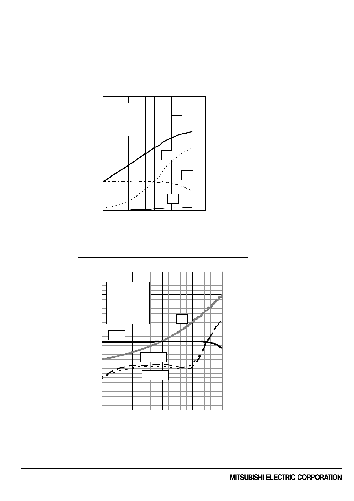
TYPICAL CHARACTERISTICS ( 380-430MHz )
(These are only typical curves and devices are not necessarily guaranteed at these curves.)
Pin-Po CHARACTERISTICS @f=380-430MHz
50
40
30
20
Ta=+25°C
f=380MHz
Vdd=7.2V
Idq=250mA
Po
η
d
Gp
100
80
60
ηd(%)
40
10
Idd
0
0 5 10 15 20 25 30
Pin(dBm)
0
Po-ACP characte r is tic
Ta=+25°C
-10
f=380MHz
-20
-30
ACP (dBc)
-40
Idq=250mA
Gain
ACP_1L
ηd
20
0
80
60
40
20
0
Publication Date : Oct.2011
ACP_1H
-50
-60
20 25 30 35 40
Po (dBm)
The detail of this application is shown in application note(AN-UHF-105.)
8
-20
-40
Page 9

< Silicon RF Power MOS FET (Discrete) >
RF-in
RF-OUT
W:line width=1.0mm
RF-in
RF-OUT
W:line width=1.0mm
RD07MUS2B
RoHS Compliance, Silicon MOSFET Power Transistor,175MHz,527MHz,870MHz,7W
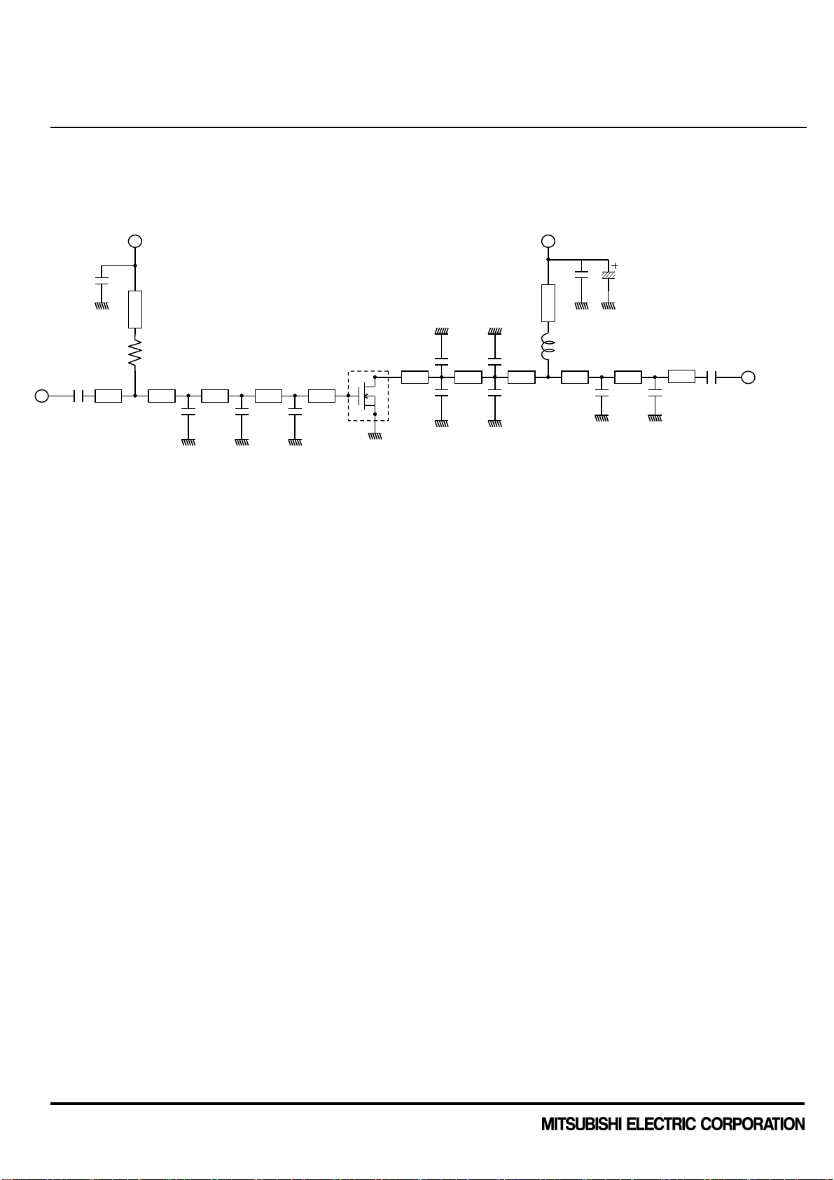
TEST CIRCUIT(f=135-175MHz)
C1
4.7K ohm
3.5mm
1.5mm 4.5mm
L5 L45.5mm 3mm
100pF
140pF
43pF
Note:Board material Glass-Epoxy substrate
Micro strip line width=1.3mm/50 ohm,er:4.8,t=0.8mm
TEST CIRCUIT(f=450-527MHz)
Vgg Vdd
21mm
W
5mm 9.5mm
2.2 ohm
RD07MUS2B
(f=135-175MHz)
L1,L2:Enameled wire 6 Turns,D:0.23mm,1.66mm O.D
L3,L5:Enameled wire 2 Turns,D:0.23mm,1.66mm O.D
L4 :Enameled wire 4 Turns,D:0.43mm,1.66mm O.D
C1,C2:1000pF,0.0022μF in parallel
7.5mm
22pF
22pF
21mm
L31mm 3mm 3mm L2 2.5mm
22μF,50V
C2
W
L1
7.5mm
3.5mm
100pF
20pF
2.5mm
62pF
100pF
Vgg Vdd
C1
21mm
W
4.7K ohm
4mm
10mm 4mm
12pF
8pF
Note:Board material Glass-Epoxy substrate
Micro strip line width=1.3mm/50 ohm,er:4.8,t=0.8mm
5mm 1mm
8pF 12pF 5 4pF
5.5mm 1mm
RD07MUS2B
(f=450-527MHz)
3mm
L1:Enameled wire 5 Turns,D:0.43mm,2.46mm O.D
L2:Enameled wire 2 Turns,D:0.23mm,1.66mm O.D
C1,C2:1000pF,0.0022μF in parallel
4.5mm 6mm L2 7.5mm
24pF
21mm
22μF,50V
C2
W
L1
0.5mm
2.5mm
9pF24pF
8pF
5.5mm
100pF
Publication Date : Oct.2011
9
Page 10
< Silicon RF Power MOS FET (Discrete) >
RF-in
RF-OUT
W:line width=1.0mm
RD07MUS2B
RoHS Compliance, Silicon MOSFET Power Transistor,175MHz,527MHz,870MHz,7W
TEST CIRCUIT(f=763-870MHz)
150pF
C1
4.7K ohm
19mm
Vgg Vdd
21mm
W
RD07MUS2B
(f=763-870MHz)
9mm 1.5mm
2.5mm 1mm
1pF 6pF 12pF
Note:Board material Glass-Epoxy substrate
Micro strip line width=1.3mm/50 ohm,er:4.8,t=0.8mm
10pF 8pF
0.5mm
1mm 12mm
10pF
L1:Enameled wire 7 Turns,D:0.23mm,1.66mm O.D
C1,C2:1000pF,100pF in parallel
21mm
22μF,50V
C2
W
L1
1mm
1mm
6pF8pF
16.5mm
150pF
1pF
Publication Date : Oct.2011
10
Page 11
< Silicon RF Power MOS FET (Discrete) >
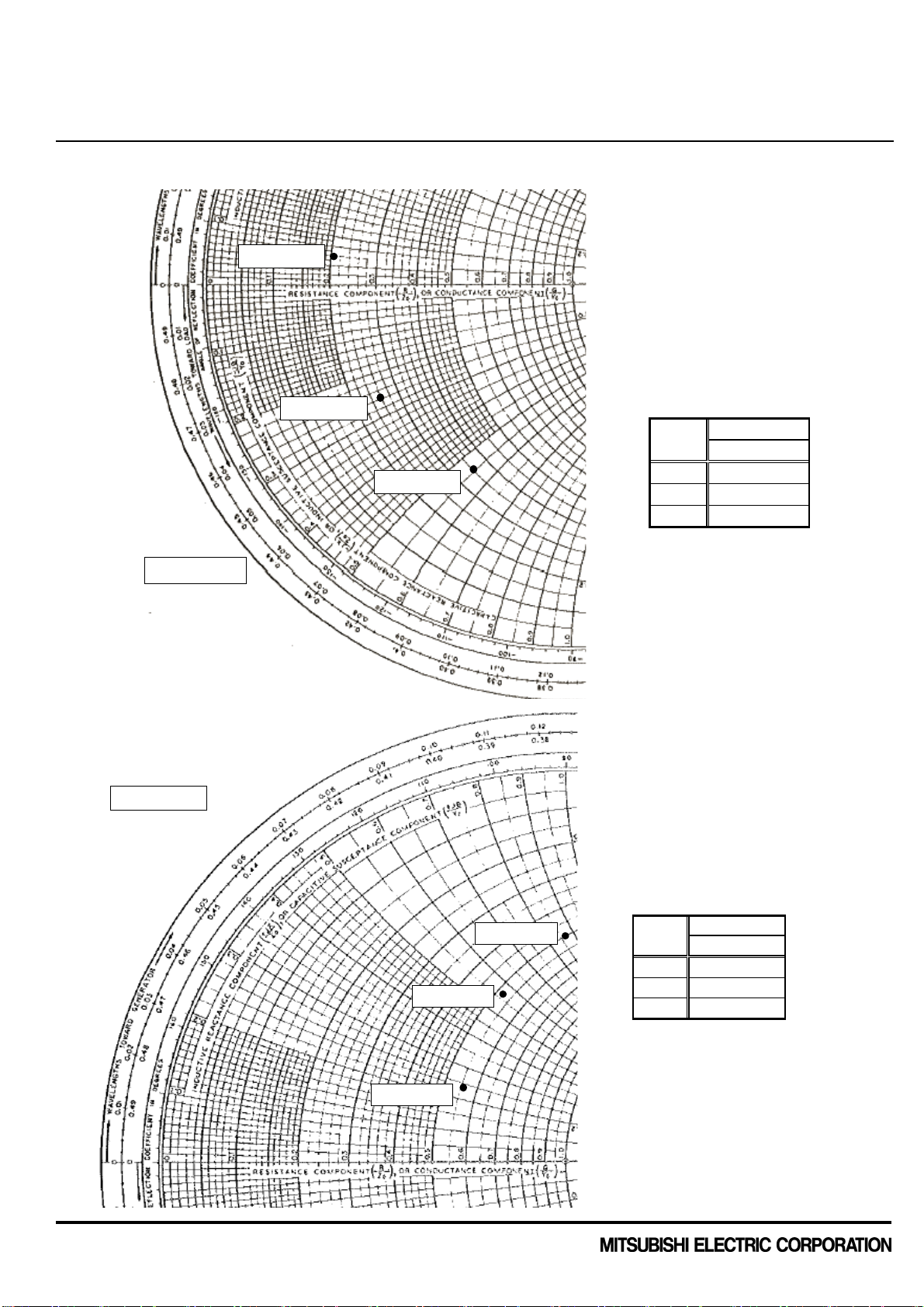
f
Zin*
(MHz)
(ohm)
135
5.58+j2.43
155
5.25+j5.60
175
5.01+j8.65
f
Zout*
(MHz)
(ohm)
135
3.50-j5.54
155
2.57-j2.57
175
2.06+j0.62
Zout*: Complex conjugate of
RD07MUS2B
RoHS Compliance, Silicon MOSFET Power Transistor,175MHz,527MHz,870MHz,7W
Input / Output Impedance VS. Frequency Characteristics
f=175MHz
Zo=10ohm
Zout* ( f=135, 155, 175MHz)
@Pin=0.3W, Vdd=7.2V,
Idq=250mA(Vgg adj.)
f=155MHz
f=135MHz
output impedance
Zin* ( f=135, 155, 175MHz)
Zo=10ohm
@Pin=0.3W, Vdd=7.2V,
Idq=250mA(Vgg adj.)
f=175MHz
f=155MHz
f=135MHz
Zin*: Complex conjugate of
input impedance
Publication Date : Oct.2011
11
Page 12
< Silicon RF Power MOS FET (Discrete) >
f
Zin*
(MHz)
(ohm)
450
2.62+j2.02
490
2.90+j3.07
520
3.29+j3.70
527
3.40+j3.81
f
Zout*
(MHz)
(ohm)
450
2.80+j1.07
490
2.25+j0.75
520
1.51+j1.04
527
1.36+j1.20
Zout*: Complex conjugate of
RD07MUS2B
RoHS Compliance, Silicon MOSFET Power Transistor,175MHz,527MHz,870MHz,7W
Input / Output Impedance VS. Frequency Characteristics
Zout* ( f=450, 490, 520, 527MHz)
@Pin=0.4W, Vdd=7.2V,
Zo=10ohm
Idq=250mA(Vgg adj.)
f=527MHz
f=520MHz
Zin* ( f=450, 490, 520, 527MHz)
Zo=10ohm
f=450MHz
f=485MHz
f=520MHz
f=490MHz
output impedance
@Pin=0.4W, Vdd=7.2V,
Idq=250mA(Vgg adj.)
f=527MHz
Publication Date : Oct.2011
f=450MHz
Zin*: Complex conjugate of
input impedance
12
Page 13
< Silicon RF Power MOS FET (Discrete) >
f
Zin*
(MHz)
(ohm)
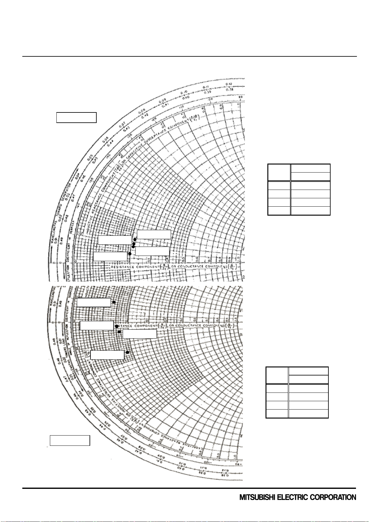
763
1.72-j1.54
806
1.55-j0.50
817
1.46-j0.23
870
1.28+j0.95
f
Zout*
(MHz)
(ohm)
763
2.01+j0.43
806
2.16+j0.80
817
2.17+j0.85
870
2.17+j1.07
Zout*: Complex conjugate of
RD07MUS2B
RoHS Compliance, Silicon MOSFET Power Transistor,175MHz,527MHz,870MHz,7W
Input / Output Impedance VS. Frequency Characteristics
Zout* ( f=763, 806, 817, 870MHz)
Zo=10ohm
f=817MHz
f=763MHz
@Pin=0.5W, Vdd=7.2V,
Idq=250mA(Vgg adj.)
f=870MHz
f=806MHz
output impedance
f=870MHz
f=817MHz
f=763MHz
Zo=10ohm
Zin* ( f=763, 806, 817, 870MHz)
@Pin=0.5W, Vdd=7.2V,
Idq=250mA(Vgg adj.)
f=806MHz
Zin*: Complex conjugate of
input impedance
Publication Date : Oct.2011
13
Page 14

< Silicon RF Power MOS FET (Discrete) >
RD07MUS2B S-PARAMETER DATA (@Vdd=7.2V, Id=250mA)
Freq.
[MHz]
(mag)
(ang)
(mag)
(ang)
(mag)
(ang)
(mag)
(ang)
100
0.850
-170.8
10.060
79.2
0.016
-9.1
0.745
-168.8
135
0.857
-173.2
7.300
73.1
0.016
-14.2
0.759
-169.5
150
0.858
-173.7
6.509
70.7
0.015
-15.2
0.763
-170.0
175
0.863
-174.6
5.435
66.9
0.015
-18.8
0.773
-170.7
200
0.871
-175.4
4.687
63.5
0.014
-23.8
0.781
-170.6
250
0.881
-176.8
3.556
56.7
0.013
-27.4
0.806
-171.0
300
0.889
-178.1
2.791
51.2
0.013
-32.8
0.825
-171.7
350
0.903
-179.0
2.261
45.7
0.011
-36.7
0.843
-172.4
400
0.910
-180.0
1.861
40.9
0.010
-39.7
0.859
-173.2
450
0.918
178.8
1.559
36.7
0.009
-41.9
0.874
-173.9
500
0.927
177.7
1.320
33.0
0.008
-44.9
0.888
-174.5
520
0.928
177.2
1.236
31.5
0.008
-45.1
0.893
-174.8
527
0.929
177.2
1.212
31.2
0.008
-44.2
0.894
-174.9
550
0.931
176.7
1.130
29.5
0.008
-46.4
0.896
-175.4
600
0.934
175.6
0.974
26.5
0.007
-46.4
0.909
-176.0
650
0.940
174.4
0.848
23.4
0.006
-48.0
0.915
-176.5
700
0.943
173.5
0.745
20.9
0.005
-46.0
0.921
-177.4
750
0.946
172.6
0.660
18.6
0.005
-45.9
0.928
-177.8
763
0.948
172.3
0.638
18.0
0.004
-44.9
0.931
-178.0
800
0.950
171.5
0.587
16.5
0.004
-42.0
0.931
-178.3
806
0.951
171.7
0.578
16.3
0.004
-45.4
0.931
-178.3
817
0.950
171.3
0.563
15.8
0.004
-43.6
0.933
-178.6
850
0.950
170.8
0.522
14.5
0.003
-41.8
0.934
-178.8
870
0.955
170.6
0.502
13.8
0.003
-39.4
0.935
-178.9
900
0.952
170.0
0.471
12.9
0.003
-33.7
0.941
-179.2
950
0.956
169.2
0.427
11.1
0.002
-26.6
0.943
-179.5
1000
0.957
168.4
0.387
9.7
0.002
-17.3
0.943
179.9
1050
0.960
167.7
0.353
8.1
0.002
-7.4
0.949
179.7
1100
0.961
167.1
0.323
6.9
0.002
8.9
0.949
179.6
RD07MUS2B
RoHS Compliance, Silicon MOSFET Power Transistor,175MHz,527MHz,870MHz,7W
S11 S21 S12 S22
Publication Date : Oct.2011
14
Page 15

< Silicon RF Power MOS FET (Discrete) >
RD07MUS2B S-PARAMETER DATA (@Vdd=3.6V, Id=250mA)
Freq.
[MHz]
(mag)
(ang)
(mag)
(ang)
(mag)
(ang)
(mag)
(ang)
100
0.850
-172.3
8.581
78.7
0.016
-9.3
0.782
-171.0
135
0.855
-174.2
6.239
73.0
0.016
-13.3
0.793
-171.6
150
0.856
-174.7
5.564
70.6
0.016
-17.3
0.797
-172.0
175
0.862
-175.3
4.661
66.8
0.015
-20.0
0.806
-172.5
200
0.869
-176.2
4.030
63.5
0.015
-23.1
0.812
-172.7
250
0.881
-177.4
3.057
56.8
0.014
-28.7
0.831
-173.0
300
0.887
-178.5
2.400
51.3
0.013
-32.8
0.849
-173.6
350
0.901
-179.5
1.945
46.0
0.012
-36.0
0.863
-174.3
400
0.909
179.6
1.606
41.2
0.010
-40.7
0.877
-175.0
450
0.917
178.6
1.345
37.2
0.009
-42.4
0.890
-175.5
500
0.927
177.5
1.139
33.2
0.008
-45.0
0.902
-176.2
520
0.929
177.0
1.068
31.9
0.008
-45.4
0.904
-176.3
527
0.926
176.9
1.048
31.6
0.008
-44.5
0.907
-176.4
550
0.929
176.4
0.975
29.9
0.008
-45.1
0.909
-176.9
600
0.933
175.3
0.841
26.9
0.007
-47.2
0.918
-177.4
650
0.937
174.2
0.732
23.8
0.006
-47.4
0.925
-178.0
700
0.944
173.4
0.644
21.4
0.005
-46.7
0.931
-178.6
750
0.945
172.5
0.571
19.2
0.005
-44.2
0.935
-179.0
763
0.947
172.2
0.552
18.4
0.005
-44.2
0.939
-179.1
800
0.949
171.6
0.508
17.0
0.004
-43.7
0.938
-179.3
806
0.949
171.5
0.502
16.8
0.004
-42.8
0.938
-179.5
817
0.951
171.4
0.488
16.2
0.004
-42.3
0.940
-179.6
850
0.949
170.8
0.454
15.0
0.003
-40.8
0.941
-179.8
870
0.953
170.5
0.436
14.3
0.003
-37.7
0.940
-180.0
900
0.952
169.9
0.408
13.3
0.003
-32.1
0.946
179.8
950
0.957
169.2
0.370
11.8
0.003
-25.2
0.949
179.5
1000
0.959
168.2
0.335
10.3
0.002
-18.0
0.949
179.0
1050
0.960
167.7
0.306
8.6
0.002
-6.7
0.955
178.8
1100
0.960
167.0
0.280
7.4
0.002
6.9
0.954
178.7
RD07MUS2B
RoHS Compliance, Silicon MOSFET Power Transistor,175MHz,527MHz,870MHz,7W
S11 S21 S12 S22
Publication Date : Oct.2011
15
Page 16

< Silicon RF Power MOS FET (Discrete) >
RD07MUS2B
RoHS Compliance, Silicon MOSFET Power Transistor,175MHz,527MHz,870MHz,7W
APPLICATION-NOTE
Typical Characteristics Table (Application For Example)
(These are only typical value and devices are not necessarily guaranteed at these values.)
RD07MUS2B
Single-stage amplifier for analog radio solution
Application Note Frequency Band Vds Pin Po Gp η
AN-VHF-047 135 to 175MHz 7.2V 0.3W 7W 13.7dB 65%
AN-VHF-046 170 to 205MHz 7.2V 0.3W 7W 13.7dB 70%
AN-UHF-096 450 to 527MHz 7.2V 0.4W 7W 12.4dB 66%
AN-UHF-098 400 to 470MHz 7.2V 0.4W 7W 12.5dB 60%
AN-900-039 763 to 870MHz 7.2V 0.5W 6.5W 11.1dB 53%
Single-stage amplifier for digital radio solution
Application Note Frequency Band Vds Pin Po Gp ηd ACP
AN-UHF-105 380 to 430MHz 7.2V 0.03W 3W 19.7dB 35% -39dBc
AN-UHF-106 350 to 400MHz 7.2V 0.03W 3W 19.5dB 32% -40dBc
AN-900-041 800 to 870MHz 3.6V 0.04W 1W 12.2dB 32% -34dBc
RD01MUS2 RD07MUS2B
or RD01MUS1
2stage(RD07MUS2B with dirver PA) amplifier for analog radio solution
d
Application Note Frequency Band Vds Pin Po Gp ηd
AN-VHF-053 135 to 175MHz 7.2V 0.03W 7.1W 23.7dB 47%
AN-UHF-097 400 to 470MHz 7.2V 0.03W 7W 23.6dB 55%
AN-UHF-115 450 to 530MHz 7.2V 0.03W 7.4W 23.9dB 45%
AN-900-040 763 to 870MHz 7.2V 0.03W 7.2W 23.8dB 53%
2stage(RD07MUS2B with dirver PA) amplifier for digital radio solution
Application Note Frequency Band Vds Pin Po Gp η
AN-UHF-116 380 to 430MHz 7.2V 0.001W 3W 34.9dB 32% -39dBc
Publication Date : Oct.2011
16
d
ACP
Page 17

< Silicon RF Power MOS FET (Discrete) >
have
until cold after switch
his products without cause damage for human and
details
copies of the formal
(RF power transistors) are designed
other applications.
In particular, while these products are highly reliable for their designed purpose, they are not manufactured
quality assurance testing protocol that is sufficient to guarantee the level of reliability typically deemed
In the application, which is base station applications and
off frequency
during transmitting, please consider the derating, the redundancy system, appropriate setting of the maintain
predicted operating life time of
an authorized Mitsubishi
therefore
device is
It is
sink in conjunction with other cooling methods as needed (fan,
lower than 120deg/C(in case of
6. Do not use the device at the exceeded the maximum rating condition. In case of plastic molded devices, the
exceeded maximum rating condition may cause blowout, smoldering or catch fire of the molding resin due to
extreme short current flow between the drain and the source of the device. These results causes in fire or
the
Warranty for the product is void if the products protective cap (lid) is removed or if the product is modified in
, please refer the last page
RD07MUS2B
RoHS Compliance, Silicon MOSFET Power Transistor,175MHz,527MHz,870MHz,7W
ATTENTION:
1.High Temperature ; This product might have a heat generation while operation,Please take notice that
a possibility to receive a burn to touch the operating product directly or touch the product
off. At the near the product,do not place the combustible material that have possibilities to arise the fire.
2.Generation of High Frequency Power ; This product generate a high frequency power. Please take notice
that do not leakage the unnecessary electric wave and use t
property per normal operation.
3.Before use; Before use the product,Please design the equipment in consideration of the risk for human and
electric wave obstacle for equipment.
PRECAUTIONS FOR THE USE OF MITSUBISHI SILICON RF POWER DEVICES:
1. The specifications of mention are not guarantee values in this data sheet. Please confirm additional
regarding operation of these products from the formal specification sheet. For
specification sheets, please contact one of our sales offices.
2.RA series products (RF power amplifier modules) and RD series products
for consumer mobile communication terminals and were not specifically designed for use in
under a
necessary for critical communications elements and
fixed station applications that operate with long term continuous transmission and a higher on-
period and others as needed. For the reliability report which is described about
Mitsubishi Silicon RF Products , please contact Mitsubishi Electric Corporation or
Semiconductor product distributor.
3. RD series products use MOSFET semiconductor technology. They are sensitive to ESD voltage
appropriate ESD precautions are required.
4. In the case of use in below than recommended frequency, there is possibility to occur that the
deteriorated or destroyed due to the RF-swing exceed the breakdown voltage.
5. In order to maximize reliability of the equipment, it is better to keep the devices temperature low.
recommended to utilize a sufficient sized heatetc.) to keep the channel temperature for RD series products
Tchmax=150deg/C) ,140deg/C(in case of Tchmax=175deg/C) under standard conditions.
injury.
7. For specific precautions regarding assembly of these products into the equipment, please refer to
supplementary items in the specification sheet.
8.
any way from it’s original form.
9. For additional “Safety first” in your circuit design and notes regarding the materials
of this data sheet.
10. Please refer to the additional precautions in the formal specification sheet.
Publication Date : Oct.2011
17
Page 18

< Silicon RF Power MOS FET (Discrete) >
RD07MUS2B
RoHS Compliance, Silicon MOSFET Power Transistor,175MHz,527MHz,870MHz,7W
Keep safety first in your circuit designs!
Mitsubishi Electric Corporation puts the maximum effort into making semiconductor products better and more
reliable, but there is always the possibility that trouble may occur with them. Trouble with semiconductors may lead
to personal injury, fire or property damage. Remember to give due consideration to safety when making your circuit
designs, with appropriate measures such as (i) placement of substitutive, auxiliary circuits, (ii) use of
non-flammable material or (iii) prevention against any malfunction or mishap.
Notes regarding these materials
•These materials are intended as a reference to assist our customers in the selection of the Mitsubishi
semiconductor product best suited to the customer’s application; they do not convey any license under any
intellectual property rights, or any other rights, belonging to Mitsubishi Electric Corporation or a third party.
•Mitsubishi Electric Corporation assumes no responsibility for any damage, or infringement of any third-party’s
rights, originating in the use of any product data, diagrams, charts, programs, algorithms, or circuit application
examples contained in these materials.
•All information contained in these materials, including product data, diagrams, charts, programs and algorithms
represents information on products at the time of publication of these materials, and are subject to change by
Mitsubishi Electric Corporation without notice due to product improvements or other reasons. It is therefore
recommended that customers contact Mitsubishi Electric Corporation or an authorized Mitsubishi Semiconductor
product distributor for the latest product information before purchasing a product listed herein.
The information described here may contain technical inaccuracies or typographical errors. Mitsubishi Electric
Corporation assumes no responsibility for any damage, liability, or other loss rising from these inaccuracies or
errors.
Please also pay attention to information published by Mitsubishi Electric Corporation by various means, including
the Mitsubishi Semiconductor home page (http://www.MitsubishiElectric.com/).
•When using any or all of the information contained in these materials, including product data, diagrams, charts,
programs, and algorithms, please be sure to evaluate all information as a total system before making a final
decision on the applicability of the information and products. Mitsubishi Electric Corporation assumes no
responsibility for any damage, liability or other loss resulting from the information contained herein.
•Mitsubishi Electric Corporation semiconductors are not designed or manufactured for use in a device or system
that is used under circumstances in which human life is potentially at stake. Please contact Mitsubishi Electric
Corporation or an authorized Mitsubishi Semiconductor product distributor when considering the use of a product
contained herein for any specific purposes, such as apparatus or systems for transportation, vehicular, medical,
aerospace, nuclear, or undersea repeater use.
•The prior written approval of Mitsubishi Electric Corporation is necessary to reprint or reproduce in whole or in part
these materials.
•If these products or technologies are subject to the Japanese export control restrictions, they must be exported
under a license from the Japanese government and cannot be imported into a country other than the approved
destination.
Any diversion or re-export contrary to the export control laws and regulations of Japan and/or the country of
destination is prohibited.
•Please contact Mitsubishi Electric Corporation or an authorized Mitsubishi Semiconductor product distributor for
further details on these materials or the products contained therein.
© 2011 MITSUBISHI ELECTRIC CORPORATION. ALL RIGHTS RESERVED.
Publication Date : Oct.2011
18
 Loading...