

< Silicon RF Power MOS FET (Discrete) >
RD02MUS2
RoHS Compliance,Silicon MOSFET Power Transistor 175MHz,520MHz,2W
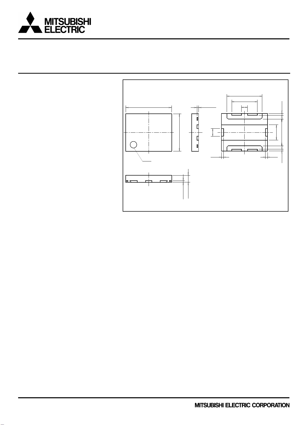
OUTLINE DRAWING
DESCRIPTION
RD02MUS2 is a MOS FET type transistor
specifically designed for VHF/UHF RF power
amplifiers applications.
This device has an internal monolithic zener
diode from gate to source for ESD protection.
FEATURES
•High power gain:
Pout>2W, Gp>16dB
@Vdd=7.2V,f=175MHz, 520MHz
•High Efficiency: 65%typ. (175MHz)
•High Efficiency: 65%typ. (520MHz)
6.0+/-0.15
INDEX MARK
(Gate)
4.9+/-0.15
0.9+/-0.1
0.2+/-0.05
0.2+/-0.05
1.0+/-0.05
(0.25)
4.6+/-0.05
3.3+/-0.05
0.8+/-0.05
1
2
3
Terminal No.
1.Drain (output)
2.Source (GND)
3.Gate (input)
Note
( ):center value
UNIT:mm
(0.25)
2.0+/-0.05
3.5+/-0.05
(0.22) (0.22)
•Integrated gate protection diode
APPLICATION
For output stage of high power amplifiers
In VHF/UHF band mobile radio sets.
RoHS COMPLIANT
RD02MUS2-101,T112 is a RoHS compliant products.
RoHS compliance is indicating by the letter “G” after the Lot Marking.
This product includes the lead in high melting temperature type solders.
However, it is applicable to the following exceptions of RoHS Directions.
1.Lead in high melting temperature type solders (i.e.tin-lead solder alloys containing more than85% lead.)
Publication Date : Oct.2011
1
< Silicon RF Power MOS FET (Discrete) >
RD02MUS2
RoHS Compliance,Silicon MOSFET Power Transistor 175MHz,520MHz,2W
ABSOLUTE MAXIMUM RATINGS
(Tc=25°CUNLESS OTHERWISE NOTED)
SYMBOL PARAMETER CONDITIONS RATINGS UNIT
VDSS Drain to source voltage Vgs=0V 30 V
VGSS Gate to source voltage Vds=0V -5/+10 V
Pch Channel dissipation Tc=25
Pin Input Power Zg=Zl=50
ID Drain Current - 1.5 A
Tch Junction temperature - 150
Tstg Storage temperature - -40 to +125
Rth j-c Thermal resistance Junction to case 5.7
Note: Above parameters are guaranteed independently.
°C
21.9 W
0.1 W
°C
°C
°C/W
ELECTRICAL CHARACTERISTICS (Tc=25°C, UNLESS OTHERWISE NOTED)
SYMBOL PARAMETER CONDITIONS
I
DSS
I
GSS
Zero gate Voltage drain current VDS=17V, VGS=0V - - 100 uA
Gate to source leak current VGS=10V, VDS=0V - - 1 uA
LIMITS UNIT
MIN TYP MAX.
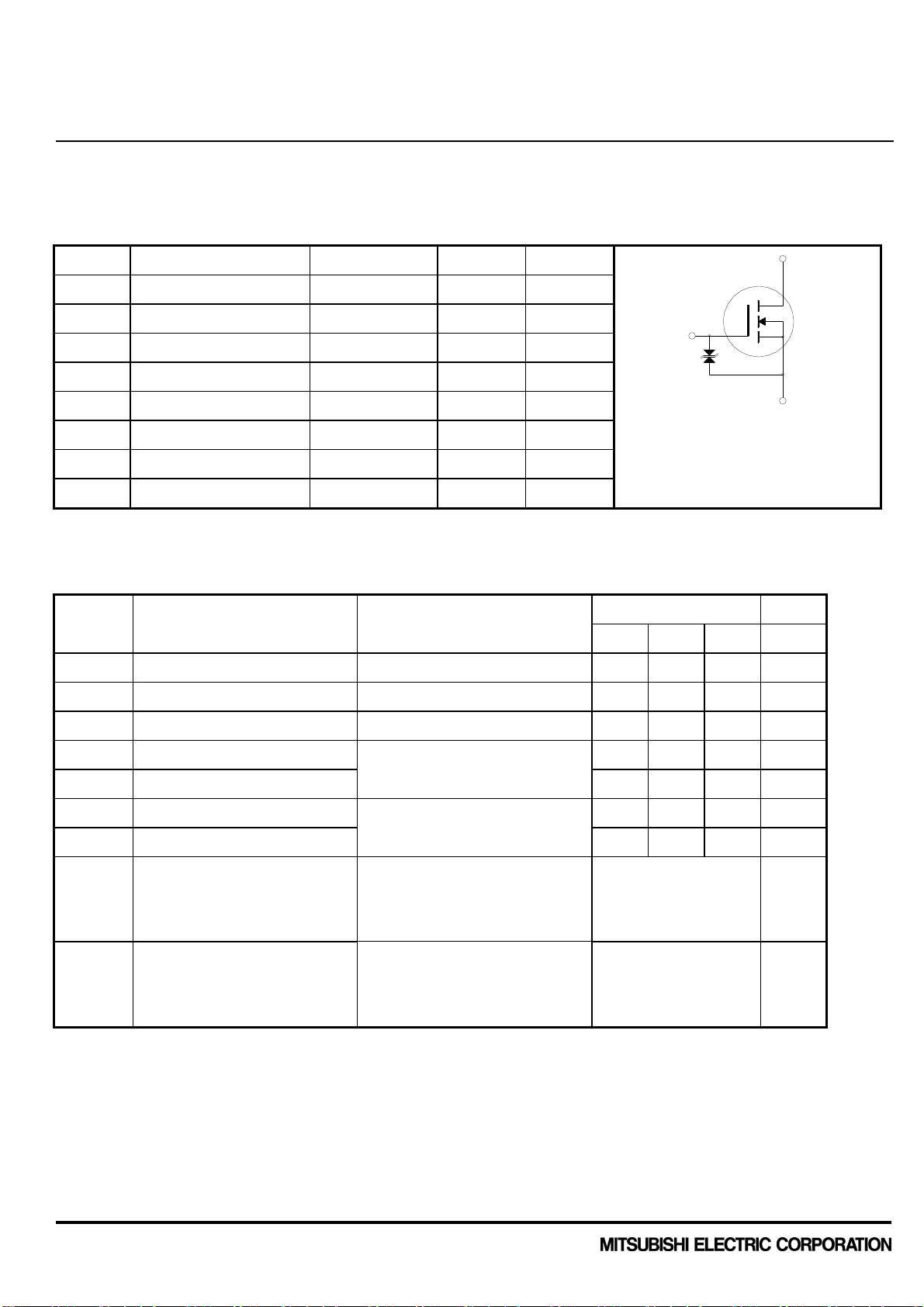
D
G
S
SCHEMATIC DRAWING
V
Pout1 Output power 2 3 - W
Pout2 Output power 2 3 - W
Note: Above parameters, ratings, limits and conditions are subject to change.
Gate threshold Voltage VDS=12V, IDS=1mA 1 1.8 3 V
th
VDD=7.2V, Pin=50mW,
Drain efficiency
D1
Drain efficiency
D2
Load VSWR tolerance
Load VSWR tolerance
f=175MHz Idq=200mA
VDD=7.2V, Pin=50mW,
f=520MHz Idq=200mA
VDD=9.2V,Po=2W(Pin Control)
f=175MHz,Idq=200mA,Zg=50
Load VSWR=20:1(All Phase)
VDD=9.2V,Po=2W(Pin Control)
f=520MHz,Idq=200mA,Zg=50
Load VSWR=20:1(All Phase)
55 65 - %
50 65 - %
No destroy -
No destroy -
Publication Date : Oct.2011
2
< Silicon RF Power MOS FET (Discrete) >
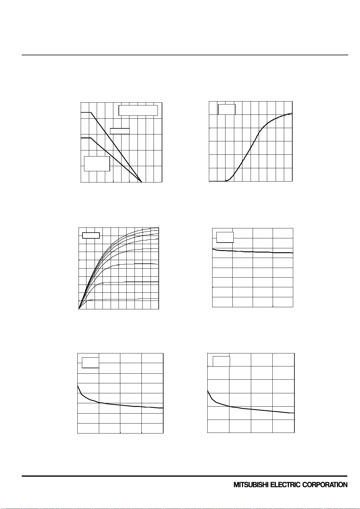
Ciss(pF)
Coss(pF)
Crss (pF)
CHANNEL DISSIPATION Pch(W)
RD02MUS2
RoHS Compliance,Silicon MOSFET Power Transistor 175MHz,520MHz,2W
TYPICAL CHARACTERISTICS
CHANNEL DISSIPATION VS.
25
...
AMBIENT TEMPERATURE
*1:The material of thePCB
Glass epoxy( t=0.8 mm)
20
15
On heat-sink
10
On PCB (*1)
withthrough hole
5
and Heat-sink
0
0 40 80 120 160 200
AMBIENT TEMPERATURETa(deg:C.)
Vds-Ids CHARACTERISTICS
5.0
Ta=+25°C
4.5
4.0
3.5
3.0
2.5
Ids(A)
2.0
1.5
1.0
0.5
0.0
0 2 4 6 8 10
Vds( V)
Vgs=10V
Vgs=9V
Vgs=8V
Vgs=7V
Vgs=6V
Vgs=5V
Vgs=4V
Vgs=3V
Vgs -Ids CHARACTERISTICS
6
Ta=+25°C
Vds=7.2V
5
4
3
Ids(A)
2
1
0
0 2 4 6 8 10
Vgs(V)
Vds VS. Ciss CHARACTERISTICS
40
Ta=+25°C
f=1MHz
30
20
10
0
0 5 10 15 20
Vds( V)
Publication Date : Oct.2011
Vds VS. Cos s CHARACTERISTICS
40
Ta=+25°C
f=1MHz
30
20
10
0
0 5 10 15 20
Vds(V)
Vds VS. Crs s CHARACTERISTICS
6
Ta=+25°C
f=1MHz
5
4
3
2
1
0
0 5 10 15 20
Vds( V)
3
 Loading...