


C
MIT
SUBIS
C
HI ELECTRI
MELSEC System Q
Programmable Logic Controllers
User’s Manual
Art. no.: 130027
05 02 2003
SH (NA)-080036-E
Version E
High-Speed Counter Module
QD62, QD62E, QD62D,
GX Configurator-CT
(SW0D5C-QCTU-E)
MITSUBISHI ELECTRI
INDUSTRIAL AUTOMATION
SAFETY PRECAUTIONS
•
(Always read before starting use.)
Before using this product, please read this manual introduced in this manual carefully and pay full
attention to safety to handle the product correctly.
The instructions given in this manual are concerned with this product. For the safety instructions of the
programmable controller system, please read the User's Manual for the CPU module to use.
In this manual, the safety instructions are ranked as "DANGER" and "CAUTION".
•
DANGER
!
CAUTION
!
Note that the !CAUTION level may lead to a serious consequence according to t he circumstances.
Always follow the instructions of both levels because they are important to personal safety.
Please store this manual in a safe place and make it accessible when required. Alway s forward it to the
end user.
Indicates that incorrect handling may cause hazardous conditions,
resulting in death or severe injury.
Indicates that incorrect handling may cause hazardous conditions,
resulting in medium or slight personal injury or physical damage.
[DESIGN PRECAUTIONS]
!
DANGER
Do not write data into the "system area" of the buffer memory of intelligent function modules.
•
Writing data into the "system area" may cause a PLC system malfunction.
Depending on the malfunction of the external output transistor, there may be cases where the
•
output is ON or OFF status. Install external monitoring circuitry for output signals that may lead
to major accidents.
!
CAUTION
Do not bunch the control wires or communication cables with the main circuit or power wires, or
•
install them close to each other.
They should be installed 150 mm(5.9 inch) or more from each other.
Not doing so could result in noise that may cause malfunction.
A - 1 A - 1

[INSTALLATION PRECAUTIONS]
!
CAUTION
Use the PLC in an environment that meets the general specifications contained in the CP U
•
User's Manual.
Using this PLC in an environment outside the range of the general specificat ions may cause
electric shock, fire, malfunction, and damage to or deterioration of the product.
When installing the module, securely insert the module fixing tabs into the mountin g holes of the
•
base module while pressing the installation lever located at the bottom of the module downward.
Improper installation may result in malfunction, breakdown or the module co ming loose and
dropping. Securely fix the module with screws if it is subject to vibration during use.
Tighten the screws within the range of specified torque.
•
If the screws are loose, it may cause the module to fallout, short circuits, or malfunction.
If the screws are tightened too much, it may cause damage to the screw and/or the module,
resulting in fallout, short circuits or malfunction.
Switch all phases of the external power supply off when mounting or removing the module.
•
Not ding so may cause electric shock or damage to the module.
Do not directly touch the conductive area or electronic components of the module.
•
Doing so may cause malfunction or failure in the module.
[WIRING PRECAUTIONS]
!
CAUTION
Perform correct pressure-displacement, crimp-contact or soldering for connector wire
•
connections using the tools specified by the manufactures.
Attach connectors to the module securely.
Be careful not to let foreign matters such as sawdust or wire chips get inside the module.
•
They may cause fires, failure or malfunction.
The top surface of the module is covered with protective film to prevent foreign objects such as
•
cable offcuts from entering the module when wiring.
Do not remove this film until the wiring is complete.
Before operating the system, be sure to remove the film to provide adequate heat ventilation.
Be sure to fix communication cables or power supply cables leading from the module by placing
•
them in the duct or clamping them.
Cables not placed in the duct or without clamping may hang or shift, allow ing them to be
accidentally pulled, which may cause a module malfunctio n and cable da mage.
When removing the communication cable from the module, do not pull the cable. When
•
removing the cable with a connector, hold the connector on the side that is connected to the
modules.
Pulling the cable that is still connected to t he module may cause malfunctio n or damage t o the
module or cable.
A - 2 A - 2

[WIRING PRECAUTIONS]
!
CAUTION
Always ground the shielded cable on the encoder side (relay box).
•
Otherwise, malfunction may occur.
When wiring, be sure to verify the rated voltage of the product as well as the terminal layout. Fire
•
or failure may result if incorrect voltage is input or incorrect wiring is performed.
Connecting terminals with incorrect voltage may result in malfunction or mechanical failure.
•
[STARTUP/MAINTENANCE PRECAUTIONS]
!
CAUTION
Do not disassemble or modify the module.
•
Doing so could cause failure, malfunction, injury or fire.
Switch all phases of the external power supply off when mounting or removing the module.
•
Not doing so may cause failure or malfunction of the module.
Do not touch the connector while the power is on.
•
Doing so may cause malfunction.
Switch all phases of the external power supply off when cleaning or retightening the terminal
•
screws and module installation screws.
Not doing so may cause failure or malfunction of the module.
If the screws are loose, it may cause the module to fallout, short circuits, or malfunction.
If the screws are tightened too much, it may cause damages to the screws and/or the module,
resulting in the module falling out, short circuits or malfunct ion.
Always make sure to touch the grounded metal to discharge the electricity charged in the body,
•
etc., before touching the module.
Failure to do so may cause a failure or malfunctions of the module.
[DISPOSAL PRECAUTIONS]
!
CAUTION
When disposing of the product, handle it as industrial waste.
•
A - 3 A - 3
REVISIONS
The manual number is given on the bottom left of the back cover.
Print Date Manual Number Revision
Dec., 1999 SH(NA)-080036-A First edition
Oct., 2000 SH(NA)-080036-B
Correction
About the Generic Terms and Abbreviation, Section 2.1, Section 7.2.2,
7.3.3, 7.6.1
Jun., 2001 SH(NA)-080036-C
Standardize the name from software package (GPP function) to
Product name (GX Developer).
Standardize the name from utility package (QCTU) to Product name
(GX Configurator-CT).
Addition
Section 2.2, 2.3
Correction
Safety Precautions, Conformation to the EMC Directive and Low
Voltage Instruction, About the Generic Terms and Abbreviations,
Product Structure, Section 2.1, Section 3.2, 3.5, Section 6.2, Section
7.2, 7.2.1, 7.2.2, 7.3.3
Feb., 2002 SH(NA)-080036-D
Correction
About the Generic Terms and Abbreviation, Section 2.1, Section 7.2.1,
7.2.2
Feb., 2003 SH(NA)-080036-E
Correction
SAFETY PRECAUTIONS, INTRODUCTION, CONTENTS, About the
Generic Terms and Abbreviations, Section 2.1, Section 3.5, Section
4.3, Section 5.4, Section 7.2.2, Sect ion 7.3. 2, Sec ti on 7.3. 3, Sec tio n 7.4
to Section 7.6, Section 8.1.1, INDEX
Japanese Manual Version SH-080035-H
This manual confers no industrial property rights or any rights of any other kind, nor does it confer any patent
licenses. Mitsubishi Electric Corporation cannot be held responsible for any problems involving industrial property
rights which may occur as a result of using the contents noted in this manual.
1999 MITSUBISHI ELECTRIC CORPORATION
A - 4 A - 4

INTRODUCTION
Thank you for purchasing the MELSEC-Q series PLC.
Before using the equipment, please read this manual carefully to develop full familiarity with the functions
and performance of the Q series PLC you have purchased, so as to ensure correct use.
CONTENTS
SAFETY PRECAUTIONS..............................................................................................................................A- 1
REVISIONS...................................................................................................................... ..............................A- 4
INTRODUCTION............................................................................................................................................A- 5
CONTENTS....................................................................................................................................................A- 5
Conformation to the EMC Directive and Low Voltage Instruction ................................................................A- 8
About the Generic Terms and Abbreviations ................................................................................................A- 8
Product Structure ...........................................................................................................................................A- 8
1 OVERVIEW 1- 1 to 1- 3
1.1 Features ..................................................................................................................................................1- 2
2 SYSTEM CONFIGURATIONS 2- 1 to 2- 4
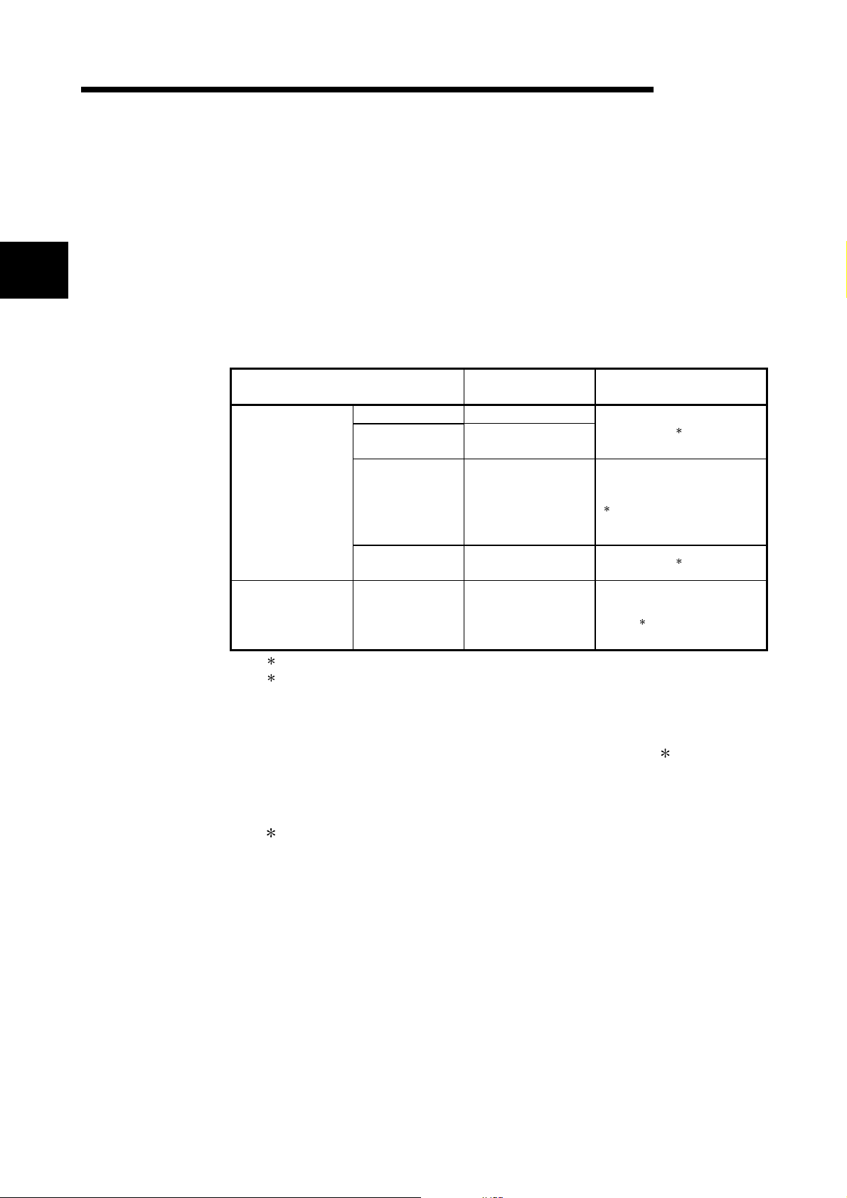
2.1 Applicable System ..................................................................................................................................2- 1
2.2 How to Check Software Version............................................................................................................. 2- 3
2.3 About Use of the QD62 (E/D) with the Q00J/Q00/Q01CPU .................................................................2- 4
3 SPECIFICATION S 3- 1 to 3-14
3.1 Performance Specifications....................................................................................................................3- 1
3.2 Function List............................................................................................................................................3- 4
3.3 I/O Signals for the PLC CPU ..................................................................................................................3- 5
3.3.1 List of I/O signals..............................................................................................................................3- 5
3.3.2 Functions of I/O signals....................................................................................................................3- 6
3.4 Buffer Memory Assignments ..................................................................................................................3- 8
3.5 Interface with External Devices ..............................................................................................................3-11
3.6 Encoders that can be Connected...........................................................................................................3-14
4 SETUP AND PROCEDURE BEFORE STARTING THE OPERATION 4- 1 to 4-16
4.1 Handling Precautions..............................................................................................................................4- 1
4.2 Procedure Before Starting the Operation............................................................................................... 4- 2
4.3 Part Identification Nomenclature ............................................................................................................4- 3
4.4 Wiring.......................................................................................................................................................4- 5
4.4.1 Wiring precautions ...............................................................................................................................4- 5
4.4.2 Wiring example of a module and a pulse generator.......................................................................4- 6
4.4.3 Wiring example of a controller and an external input terminal........................................................ 4- 8
4.4.4 Wiring example with an external output ..........................................................................................4-11
4.4.5 Using the connector/terminal block converter module.................................................................... 4-12
4.5 Switch Settings for the Intelligent Function Module...............................................................................4-14
A - 5 A - 5

5 BASIC USAGE 5- 1 to 5-11
5.1 Understanding the Pulse Input and Counting Method...........................................................................5- 1
5.1.1 Types of pulse input methods..........................................................................................................5- 1
5.1.2 Setting the count method................................................................................................................. 5- 3
5.1.3 Reading the present values.............................................................................................................5- 3
5.2 Selecting the Counter Format.................................................................................................................5- 4
5.2.1 Selecting the linear counter .............................................................................................................5- 4
5.2.2 Selecting the ring counter ................................................................................................................5- 5
5.3 Using the Coincidence Output Function................................................................................................. 5- 7
5.4 Using the Preset Function ......................................................................................................................5-10
6 CONVENIEN T US A GE 6- 1 to 6- 8
6.1 Selecting the Counter Function..............................................................................................................6- 1
6.1.1 Reading the counter function selection count value .......................................................................6- 2
6.1.2 Count error........................................................................................................................................6- 3
6.2 Using the Disable Count Function..........................................................................................................6- 4
6.3 Using the Latch Counter Function..........................................................................................................6- 5
6.4 Using the Sampling Counter Function ...................................................................................................6- 6
6.5 Using the Periodic Pulse Counter Function........................................................................................... 6- 7
7 UTILITY PACKAGE (GX Configurator-CT) 7- 1 to 7-17
7.1 Utility Package Functions........................................................................................................................7- 1
7.2 Installing and Uninstalling the Utility Package........................................................................................7- 2
7.2.1 User precautions ..............................................................................................................................7- 2
7.2.2 Operating environment.....................................................................................................................7- 4
7.3 Explanation of Utility Package Operations.............................................................................................7- 5
7.3.1 How to perform common utility package operations.......................................................................7- 5
7.3.2 Operation overview ..........................................................................................................................7- 7
7.3.3 Starting the intelligent function utility ...............................................................................................7- 9
7.4 Initial Settings..........................................................................................................................................7-11
7.5 Auto Refresh ...........................................................................................................................................7-13
7.6 Monitor/Test ............................................................................................................................................7-15
7.6.1 Monitor/Test......................................................................................................................................7-15
8 PROGRAMMING 8- 1 to 8- 9
8.1 Program Example When GX Configurator-CT is Used .........................................................................8- 2
8.1.1 Operating GX Configurator-CT........................................................................................................8- 2
8.1.2 Program example.............................................................................................................................8- 4
8.2 Program Example when GX Configurator-CT is not Used....................................................................8- 6
8.3 Example of a Program Using the Coincidence Detection Interrupt Function .......................................8- 9
A - 6 A - 6

9 TROUBLESHOOTING 9- 1 to 9- 2
9.1 Error Information .....................................................................................................................................9- 1
9.2 The Count Operation is not Working......................................................................................................9- 2
9.3 The Count Value is not Normal ..............................................................................................................9- 2
APPENDIX App- 1 to App- 2
Appendix 1 External Dimension Diagram ................................................................................................App- 1
Appendix 2 Difference Between A1SD62, A1SD62E and A1SD62D (S1).............................................App- 2
INDEX Index- 1 to Index- 2
A - 7 A - 7
Conformation to the EMC Directive and Low Voltage Instruction
For details on making Mitsubishi PLC conform to the EMC directive and low voltage
instruction when installin g it in your pro duct, ple as e see Cha pter 3, "EM C Dir ec tive
and Low Voltage Instruction" of the User's Manual (Hardware) of the PLC CPU to
use.
The CE logo is printed on the rating plate on the main body of the PLC that conforms
to the EMC directive and low voltage instruction.
By making this product conform to the EMC directive and low voltage instruction, it is
not necessary to make those steps individually.
About the Generic Terms and Abbreviations
Unless otherwise specified, this manual uses the following generic terms and
abbreviations to describe the Type QD62, QD62D and QD62E high-speed counter
module.
Generic Term/Abbreviation Description of the abbreviation/general terms
DOS/V personal computer DOS/V-compatible personal computer of IBM PC/AT® and its compatible
Generic product name of the product types SWnD5C-GPPW-E, SWnD5C-GPPW-EA,
GX Developer
QCPU (Qmode)
GX Configurator-CT
QD62 Abbreviation of the Type QD62 high-speed counter module
QD62E Abbreviation of the Type QD62E high-speed counter module
QD62D Abbreviation of the Type QD62D high-speed counter module
QD62(E/D) Generic term of QD62, QD62E and QD62D
SWnD5C-GPPW-EV and SWnD5C-GPPW-EVA.
"n" in the model name is 4 or greater.
Generic term of Q00JCPU, Q00CPU, Q01CPU, Q02CPU, Q02HCPU, Q06HCPU,
Q12HCPU, Q25HCPU, Q12PHCPU, Q25PHCPU
Generic term of counter module setting/monitor tool GX Configurator-CT (SW0D5CQCTU-E)
Product Structure
The product structure of this product is given in the table below.
Model Name Product Name Quantity
QD62 Type QD62 high-speed counter module 1
QD62E Type QD62E high-speed counter module 1
QD62D Type QD62D high-speed counter module 1
SW0D5C-QCTU-E GX Configurator-CT Version 1 (1-license product) (CD-ROM) 1
SW0D5C-QCTU-EA GX Configurator-CT Version 1 (Multiple-license product) (CD-ROM) 1
A - 8 A - 8
1 OVERVIEW
1 OVERVIEW
MELSEC-Q
This User's Manual describes the specifications, handling and programming method
for the QD62, QD62E and QD62D high-speed counter modules (QD62 (E/D)) used
together with the MELSEC-Q series CPUs.
The QD62(E/D) modules are available with the following I/O types, maximum counting
speeds and number of channels.
Item QD62 QD62E QD62D
I/O type
Maximum counting
speed
DC input sinking
output
200 kPPS 500 kPPS
DC input sourcing
output
Differential input
sinking output
Number of channels 2 channels
The QD62(E/D) modules have the following input methods for 1 phase/2 phase pulse input:
• Phase 1 pulse input multiple of 1 • Phase 1 pulse input multiple of 2 • CW/CCW
• Phase 2 pulse input multiple of 1 • Phase 2 pulse input multiple of 2
• Phase 2 pulse input multiple of 4
See Section 5.1 for details on the input methods.
An overview of QD62 (E/ D ) ope rat ion is shown in the figure below.
4) I/O signal
Buffer memory
read/write
QD62(E/D)
PLC CPU
QCPU (Q mode)
1
Pulse generator
Encoder
Controller
Pulse generator
Encoder
Controller
Pulse
External
control signal
Preset counter
function selection
Pulse
External
control signal
Preset counter
function selection
1)
CH1
2)
3)
CH2
4)
3) Coincidence signal output (2 points)
3) Coincidence signal output (2 points)
1) Counts the pulses to be input to the QD62 (E/D).
2) Preset or counter function can be selected with an external control signal.
3) The present count value and the coincidence output point setting value can be
compared to output a coincidence signal.
4) Using the sequence program, the I/O signal and buffer memory status of the
QD62 (E/D) can be verified.
Also, count start/stop, preset, and counter function can be selected.
1 - 1 1 - 1

1 OVERVIEW
1.1 Features
MELSEC-Q
1
The features of the QD62(ED) are as follows:
(1) Counting can be performed in a wide range (The count value can be
expressed within the range between –2147483648 and 2147483647)
The count values are stored as 2-channel 32-bit signed binary codes.
(2) The maximum counting speed can be ch ang ed
The maximum speed of the QD62D can be changed by selecting from among
500 k, 200 k, 100 k and 10 k, while that of the QD62 and QD62E can be selected
from among 200k, 100k and 10k. This allows an error-free count even with
gradual rise/fall pulses.
(3) Pulse input can be selected
The pulse input can be selected from 1 phase multiple of 1, 1 phase multiple of 2,
2 phase multiple of 1, 2 phase multiple of 2, 2 phase multiple of 4, CW and CCW.
(4) Counter format can be selected
Either one of the following counter formats can be selected.
(a) Linear counter format
A count from –2147483648 to 2147483647 is possible and if the count
exceeds the range , an ov er flow will be detected.
(b) Ring counter format
Counting is performed repeatedly between the ring counter maximum value
and minimum value.
(5) Coincidence output is possible
Any channel coincidence out put point can be preset to co mpare with the present
counter value to output the ON/OFF signal out put, o r to start an int errupt pr ogram.
(6) Selection can be made from four counter functi ons
One of the following four functions can be selected.
(a) Latch counter function
This function latches the present value of the counter when the signal was
input.
(b) Sampling counter function
This function counts the pulses that were input within the preset time period
from the sign al inpu t .
(c) Periodic pulse counter function
This function stores the present and previous values of the counter at each
preset time interval while the signal is being input.
(d) Disable count function
This function i nput s a sig na l whil e e xec u ti ng the cou nt e nabl e command to
stop pulse counting.
1 - 2 1 - 2

1 OVERVIEW
MELSEC-Q
(7) The preset function/counter selection function can be executed
using an external control signal
By applying voltage to the preset terminal/function start terminal of an external
terminal, preset function/counter function selection can be executed.
(8) Easy settings using the utility package
A utility package is sold separately (GX Configurator-CT).
The utility package is not a required item. However, it can be used to set initial
settings and automatic refresh settings onscreen, reduce sequence programs,
and check settings and operating status.
(9) A blown fuse in the external output section can be de tected
A blown fuse in th e e xte r nal ou tput se ctio n can be de te ct ed ; i t is no tified by the
input signal X and the LED display on the module.
1 - 3 1 - 3
2 SYSTEM CONFIGURATIONS
2 SYSTEM CONFIGURATIONS
This chapter explains the system configuration of the QD62 (E/D).
2.1 Applicable System
MELSEC-Q
2
This section explains the applicable system.
(1) Applicable CPU and number o f modul es that can be m ounte d
The CPU module and network module (for remote I/O station) that can have the
QD62 (E/D) and the number of modules that can be mounted are listed below.
CPU module
Network module
1 See User's Manual (Function Explanation, Program Fundamentals) for the CPU module to use.
2 See Q Corresponding MELSECNET/H Network System Reference Manual (Remote I/O
network).
Applicable module
Q12PHCPU
Q25PHCPU
QJ72LP25-25
QJ72LP25G
QJ71LP25GE
Number of modules that
can be installed
Q00JCPU Maximum 16
Q00CPU
Q01CPU
Q02CPU
Q02HCPU
Q06HCPU
Q12HCPU
Q25HCPU
QJ72BR15
Maximum 24
Maximum 64
Maximum 64
Maximum 64
Can be installed in Q mode only
1
(
MELSECNET/H Remote I/O
station (
Remarks
1
(
)
)
1
(
)
2
)
(2) Mountable base unit
QD62 (E/D) can be mounted on any of the base unit’s I/O slots ( 3). However,
depending on combinations with other mounted modules and the number of
mountings, there may be cases where the power capacity is insufficient. Be sure
to consider the power capacity when mounting the module.
3 Must be inside the point number range of 1 CPU unit and network module
(for remote I/O station).
(3) Compatibility with a multiple PLC system
First read the QCPU (Q mode) User's Manual (Function Explanation, Program
Fundamentals) if the QD62 (E/D) is used with a multiple PLC system.
(a) Compatible QD62 (E/D)
In case of using the QD62 (E/D) with the multiple PLC system, there is no
restriction by the version.
(b) Intelligent function module parameters
Perform PLC write of the intelligent function module parameters to the
control PLC of the QD62 (E/D) only.
2 - 1 2 - 1
2 SYSTEM CONFIGURATIONS
(4) Software packages supported
Correspondence between systems which use QD62 (E/D) and software
packages are as shown below.
The GX Developer is necessary when using a QD62 (E/D).
Q00J/Q00/Q01CPU
Q02/Q02H/Q06H/
Q12H/Q25HCPU
Q12PH/Q25PHCPU
If installed in a MELSECNET/H
remote I/O station
Single PLC
system
Multiple PLC
system
Single PLC
system
Multiple PLC
system
Single PLC
system
Multiple PLC
system
MELSEC-Q
Software Version
GX Developer GX Configurator-CT
Version 7 or later
Version 8 or later
Version 4 or later
Version 6 or later
Version 7.10L or later
Version 6 or later
Version 1.10L or later
(cannot be used with the
SW0D5C-QCTU-E 50F or
earlier versions)
SW0D5C-QCTU-E 00A or
later
SW0D5C-QCTU-E 50F or
later
Version 1.13P or later
(cannot be used with the
SW0D5C-QCTU-E 50F or
earlier versions)
SW0D5C-QCTU-E 50F or
later
2
(5) Connector
For the QD62(D/E), the connector is sold separately.
See Section 4.3 and make separate arrangements for the connector.
2 - 2 2 - 2
2 SYSTEM CONFIGURATIONS
2.2 How to Check Software Version
This section describes how to check the GX Configurator-CT software version.
(1) How to check the GX Configurator-C T software version
The GX Configurator-CT software version can be checked in GX Developer's
"Product information" screen.
[Startup procedure]
GX Developer "Help" Product information
MELSEC-Q
Software version
(In the case of GX Developer Version 7)
REMARK
The version indi cat io n for th e GX Confi gu r ato r -C T has b een chan ge d as show n
below from the SW0D5C-QCTU-E 50F upgrade product.
Previous product Upgrade and subsequent versions
SW0D5C-QCTU-E 50F
GX Configurator-CT Version 1.10L
2 - 3 2 - 3

2 SYSTEM CONFIGURATIONS
2.3 About Use of the QD62 (E/D) with the Q00J/Q00/Q01C PU
Here, use of the QD62 (E/D) with the Q00J/Q00/Q01CPU is explained.
(1) Number of QD62 (E/D) that can be installed when the
Q00J/Q00/Q01CPU is used
See Section 2.1 concerning the number of QD62 (E/D) that can be installed
when the Q00J/Q00/Q01CPU is used.
(2) Limitations when using the Q00J/Q00/Q01CPU
(a) The coincidence detection interrupt function cannot be used.
MELSEC-Q
2 - 4 2 - 4
3 SPECIFICATIONS
3 SPECIFICATIONS
The following describes the performance specifications, I/O signals for the PLC CPU
and buffer memory specifications of the QD62(E/D).
For the general specifications of the QD62(E/D), see the User's Manual (hardware) for
the CPU module use d.
3.1 Performance Specifications
The following describes the performance specifications of the QD62(E/D):
MELSEC-Q
3
(1) QD62 (DC input sinking output type) performance specifications
Model name
Item
Counting speed switch settings 1 200 k (100 k to 200 kPPS) 100 k (10 k to 100 kPPS) 10 k (10 kPPS or less)
I/O occupied points 16 points (I/O assignment: Intelligent 16 points)
Number of channels 2 channels
Count input
signal
Counter
Coincidence
output
External
input
External
output
5V DC internal current consumption (A) 0.30
Weight (kg) 0.11
Phase 1-phase input, 2-phase input
A,
Signal level (
Counting sp eed ( max) 2 200 kPPS 100 kPPS 10 kPPS
Counting range 32-bit signed binary values (–2147483648 to 2147483647)
Model UP/DOWN Preset counter + Ring counter function
Minimum count pulse
width (µ s)
(Duty ratio 50 %)
Comparison range 32-bit signed binary values
Comparison result
Preset
Function start
Coincidence output
B) 5/12/24 V DC 2 to 5 mA
φ
φ
5
2.5 2.5
(Min. phase differential for
2-phase input: 1.25 µ s)
2 points/channel 12/24 V DC 0.5 A/1 point 2 A/1 common
(Min. phase differential for
Set value < Count value
Set value = Count value
Set value > Count value
Transistor (sinking type) output
1: The counting speed switching can be set using the intelligent function module switch.
2: Counting speed is affected by pulse rise and fall time. Possible counting speeds are shown in the following
table. Note that if a pulse that has a large rise and/or fall time is counted, a miscount may occur.
QD62
10
5 5
2-phase input: 2.5 µ s)
5/12/24 V DC
2 to 5 mA
(Min. phase differential for
2-phase input: 25 µ s)
100
50 50
Counting speed switch settings 200 k 100 k 10 k
Rise/fall time Both 1 and 2 phase input
t = 1.25 µ s or less 200 kPPS 100 kPPS 10 kPPS
t = 2.5 µ s or less 100 kPPS 100 kPPS 10 kPPS
t = 25 µ s or less
t = 500 µ s
—
——
10 kPPS 10 kPPS
500 PPS
tt
3 - 1 3 - 1
3 SPECIFICATIONS
(2) QD62E (DC input sourcing output type) per formance speci fications
MELSEC-Q
Model name
Item
Counting speed switch settings 1 200 k (100 k to 200 kPPS) 100 k (10 k to 100 kPPS) 10 k (10 kPPS or less)
I/O occupied points 16 points (I/O assignment: Intelligent 16 points)
Number of channels 2 channels
Count input
signal
Counter
Coincidence
output
External
input
External
output
5V DC internal current consumption (A) 0.33
Weight (kg) 0.11
Phase 1-phase input, 2-phase input
A,
Signal level (
Counting sp eed ( max) 2 200 kPPS 100 kPPS 10 kPPS
Counting range 32-bit signed binary values (–2147483648 to 2147483647)
Model UP/DOWN Preset counter + Ring counter function
Minimum count pulse
width (µ s)
(Duty ratio 50 %)
Comparison range 32-bit signed binary values
Comparison result
Preset
Function start
Coincidence output
B) 5/12/24 V DC 2 to 5 mA
φ
φ
5
2.5 2.5
(Min. phase differential for
2-phase input: 1.25 µ s)
Transistor (sourcing type) output : 2 points/channel
12/24 V DC 0.1 A/1 point 0.4 A/1 common
(Min. phase differential for
QD62E
10
5 5
2-phase input: 2.5 µ s)
Set value < Count value
Set value = Count value
Set value > Count value
5/12/24 V DC
2 to 5 mA
100
50 50
(Min. phase differential for
2-phase input: 25 µ s)
1: The counting spee d sw it chi ng can be se t u si ng th e in t elli ge nt fu nc tion modu le swi t ch.
2: Counting speed is affected by pulse rise and fall time. Possible counting speeds are shown in the following
table. Note that if a pulse that has a large rise and/or fall time is counted, a miscount may occur.
3
Counting speed switch settings 200 k 100 k 10 k
Rise/fall time Both 1 and 2 phase input
t = 1.25 µ s or less 200 kPPS 100 kPPS 10 kPPS
t = 2.5 µ s or less 100 kPPS 100 kPPS 10 kPPS
t = 25 µ s or less
t = 500 µ s
—
——
10 kPPS 10 kPPS
500 PPS
tt
3 - 2 3 - 2
3 SPECIFICATIONS
(3) QD62D (differential input sinking output ty pe) per formance
MELSEC-Q
specifications
Model name
Item
Counting speed switch settings 1
I/O occupied points 16 points (I/O assignment: Intelligent 16 points)
Number of channels 2 channels
Count input
signal
Counter
Coincidence
output
External
input
External
output
5 V DC internal current consumption (A) 0.38
Weight (kg) 0.12
Phase 1-phase input, 2-phase input
A,
Signal level (
Counting sp eed ( max) 2 500 kPPS 200 kPPS 100 kPPS 10 kPPS
Counting range 32-bit signed binary values (–2147483648 to 2147483647)
Model UP/DOWN Preset counter + Ring counter function
Minimum count pulse
width (µ s)
(Duty ratio 50 %)
Comparison range 32-bit signed binary values
Comparison result
Preset
Function start
Coincidence output
B)
φ
φ
(Min. phase differential for
500 k
(200 k to 500 kPPS)
Differential line driver level (Am26LS31 [manufactured by Texas Instruments] or equivalent)
2
1 1
(Min. phase differential for
2-phase input: 0.5 µ s)
(EIA Standard RS-422-A Differential Line Driver may be connected)
Transistor (sinking type) output 2 points/channel
200 k
(100 k to 200 kPPS)
5
2.5 2.5
2-phase input: 1.25 µ s)
5/12/24 V DC 2 to 5 mA
12/24 V DC 0.5 A/1 point 2 A/1 common
QD62D
100 k
(10 k to 100 kPPS)
EIA Standard RS-422-A
5 5
(Min. phase differential for
2-phase input: 2.5 µ s)
Set value < Count value
Set value = Count value
Set value > Count value
10
10 k
(10 kPPS or less)
100
50 50
(Min. phase differential for
2-phase input: 25 µ s)
1: The counting speed switching can be set using the intelligent function module switch.
2: Counting speed is affected by pulse rise and fall time. Possible counting speeds are shown in the following
table. Note that if a pulse that has a large rise and/or fall time is counted, a miscount may occur.
Counting speed switch settings 500 k 200 k 100 k 10 k
Rise/fall time Both 1 and 2 phase input
t = 0.5 µ s or less 500 kPPS 200 kPPS 100 kPPS 10 kPPS
t = 1.25 µ s or less 200 kPPS 200 kPPS 100 kPPS 10 kPPS
t = 2.5 µ s or less
t = 25 µ s or less
t = 500 µ s
—
——
———
100 kPPS 100 kPPS 10 kPPS
10 kPPS 10 kPPS
500 PPS
tt
3 - 3 3 - 3

3 SPECIFICATIONS
MELSEC-Q
3.2 Function List
The QD62(E/D) func ti on s a re li st ed below.
Name Function Reference section
Linear counter function
Ring counter function
Coincidence output function
Coincidence detection
interrupt function
Preset function
Disable count function
Latch counter function
Counter
function
selection
Sampling counter function
Periodic pulse counter
function
The functions can be used in combination. However, only either one of the linear counter function or ring
counter function can be used, and only one of the four counter functions can be selected.
Values from –2147483648 to 2147483647 can be counted. If the
count exceeds the range, this function detects an overflow.
Repeatedly executes counting between the ring counter
maximum and minimum values.
Compares the coincidence output point of any preset channel
with the present counter value, and outputs the ON/OFF signal.
Generates an interrupt signal to the PLC CPU when coincidence
is detected, and starts the interrupt program.
Rewrites the present counter value to any numeric value.
Performs preset using the sequence program or external preset
input.
Stops the pulse count while the count enable command is being
executed.
Stores the present counter value at the time the counter function
selection start command signal is input in the buffer me mory .
Counts the pulses that are input during the preset sampling time
period from the time the counter function selection start
command is input, and stores the count in the buffer memory.
While the counter function selection start command sign al is
being input, stores the present value in the buffer memory at
preset interval.
Section 5.2.1
Section 5.2.2
Section 5.3
Section 5.4
Section 6.2
Section 6.3
Section 6.4
Section 6.5
3 - 4 3 - 4
3 SPECIFICATIONS
MELSEC-Q
3.3 I/O Signals for the PLC CPU
3.3.1 List of I/O signals
The I/O signals for the QD62(E/D) PLC CPU are listed in the table below.
For the I/O numbers (X/Y) and I/O addresses indicated in this and succeeding
sections, it is assumed that the QD62(E/D) is mounted into I/O slot 0 of the standard
base module.
Input signal (Signal direction QD62(E/D) PLC CPU) Output signal (Signal direction PLC CPU QD62(E/D))
Device No. Signal name Device No. Signal name
X00 Module ready Y00 Coincidence signal No. 1 reset command
X01 Counter value large (point No. 1) Y01 Preset command
X02 Counter value coincidence (point No. 1) Y02 Coincidence signal enable command
X03 Counter v alue small (point N o. 1) Y03 Down count command
X04 External preset request detection Y04 Count enable command
X05 Counter value large (point No. 2) Y05 External preset detection reset command
X06 Counter value coincidence (point No. 2) Y06 Counter function selection start command
X07
X08 Counter value large (point No. 1) Y08 Coincidence signal No. 1 reset command
X09 Counter value coincidence (point No. 1) Y09 Preset command
X0A Counter value small (point No. 1) Y0A Coincidence signal enable command
X0B External preset request detection Y0B Down count command
X0C Counter value large (point No. 2) Y0C C ount enable co mmand
X0D Counter value coincidence (point No. 2) Y0D External preset detection reset command
X0E
X0F Fuse broken detection flag Y0F
CH1
Counter value small (point No. 2) Y07
CH2
Counter value small (point No. 2) Y0E Counter function selection start command
CH1
Coincidence signal No. 2 reset command
CH2
Coincidence signal No. 2 reset command
3 - 5 3 - 5

3 SPECIFICATIONS
3.3.2 Functions of I/O signals
The details of the I/O signals for the QD62(E/D) are listed in the table below.
(1) Input signals
MELSEC-Q
Device No.
CH1 CH2
X00 Module ready
X01 X08
X02 X09
X03 X0A
X04 X0B External preset request detection
X05 X0C
X06 X0D
X07 X0E
X0F Fuse broken detection flag
Counter value large
(point No. 1)
Counter value coincidence
(point No. 1)
Counter value small
(point No. 1)
Counter value large
(point No. 2)
Counter value coincidence
(point No. 2)
Counter value small
(point No. 2)
Signal name
QD62(E/D) PLC CPU
Description
Turns ON when the count preparation for QD62(E/D) is completed at the
time of PLC CPU power on or reset operation, and count processing is
performed.
When Module ready (X00) is OFF, count processing is not performed.
H
Turns ON when the present value (CH1: 2
coincidence output point No. 1 setting (CH1: 4H to 5H, CH2: 24H to 25H).
Turns ON when the present value = coincidence output point No. 1
setting and the present value is latched.
Turns OFF with the coincidence signal No. 1 reset command (Y 00/Y 08).
Turns ON when the present value < coincidence output point No. 1
setting.
Turns ON with a preset command signal from the external input termina l,
and the request is latched.
Turns OFF with the external preset detection reset signal (Y05/Y 0D).
Turns ON when the present value > coincidence output point No. 2
H
setting (CH1: 6
Turns ON when the present value = coincidence output point No. 2
setting and the present value is latched.
Turns OFF with the coincidence signal No. 2 reset command (Y 07/Y 0F).
Turns ON when the present value < coincidence output point No. 2
setting.
Fuse broken detection flag (X0F) turns ON when a fuse in the
coincidence signal output section is blow n.
to 7H, CH2: 26H to 27H).
to 3H, CH2: 22H to 23H) >
3 - 6 3 - 6
3 SPECIFICATIONS
(2) Output signals
MELSEC-Q
Device No.
CH1 CH2
Y00 Y08
Y01 Y09 Preset command Turns ON when the preset function is executed.
Y02 Y0A
Y03 Y0B Down count command
Y04 Y0C C ount enable co mmand Turns ON when the count operation is performed.
Y05 Y0D
Y06 Y0E
Y07 Y0F
Coincidence signal No. 1 reset
command
Coincidence signal enable
command
External preset detection reset
command
Counter function selection start
command
Coincidence signal No. 2 reset
command
Signal name
PLC CPU
QD62 (E/D)
Operation timing Description
Turns ON when the counter value coincidence (point
No. 1) signal (X02/X09) is reset.
Turns ON when the counter value coincidence signal
(X02/X09, X06/X0D) is output to the external terminal.
Turns ON when a subtraction count is executed in the
1 phase pulse input mode.
Turns ON when the external preset request detection
signal (X04/X0B) is reset.
Turns ON when counter function selection is
executed.
• Latch counter function
• Sampling counter function
• Count disable function
• Periodic pulse counter function
Turns ON when the counter value coincidence (point
No. 2) signal (X06/X0D) is reset.
REMARK
The symbols used in the operation timing column signify the following:
………
•
•
Enabled while the signal is in ON status.
………
Enabled at signal ri se (fro m OFF to ON).
3 - 7 3 - 7
3 SPECIFICATIONS
3.4 Buffer Memory Assignments (1) Buffer memory assignment list
Buffer memory assignments (without battery backup) for the QD62 (E/D) are
listed in the table below.
The initial values are set for the buffer memory when the power is turned on or
the PLC CPU is re s e t.
The contents of the buffer memory can be read/written using the FROM/TO
commands in the sequence program or the automatic refresh function of the PLC
CPU.
Address
CH1 CH2
Hexade-
cimal
H
0
H
1
H
2
H
3
H
4
H
5
H
6
H
7
H
8
H
9
H
A
H
B
H
C
H
D
H
E
H
F
H
10
H
11
H
12
H
13
H
14
H
15
H
16
H
17
H
18
to
H
1F
Decimal
Hexade-
020H32 (L)
121H33
222H34 (L)
323H35
424H36 (L)
525H37
626H38 (L)
727H39
cimal
Decimal
Preset value setting
Present value
Coincidence output point set No. 1
Coincidence output point set No. 2
828H40 Overflow detection flag 0 Read only
929H41 Counter function selection setting
38
3F
H
42 Sampling/periodic setting
H
43 Sampling/periodic counter flag
H
44 (L)
H
H
H
H
H
H
H
H
H
H
H
H
to
H
Latch count value
45
46 (L)
Sampling count value
47
48 (L)
Periodic pulse count previous value
49
50 (L)
Periodic pulse count present value
51
52 (L)
Ring counter minimum value
53
54 (L)
Ring counter maximum value
55
56
System area — —
to
63
10 2A
11 2B
12 2C
13 2D
14 2E
15 2F
16 30
17 31
18 32
19 33
20 34
21 35
22 36
23 37
24
to
31
1: The initial v alu es are set w hen th e powe r is tu rned on or th e PLC CPU is reset.
Set data
(H)
(H)
(H)
(H)
(H)
(H)
(H)
(H)
(H)
(H)
MELSEC-Q
Initial
value
0 Read/w r ite enabled
0 R ead only
0 Read/w r ite enabled
0 Read/w r ite enabled
0 R ead only
0 Read/w r ite enabled
1
Read/write
3 - 8 3 - 8
3 SPECIFICATIONS
(2) Preset value setting (Buffer memory addr esses CH 1: 0H to1 H,
MELSEC-Q
CH2: 20H to 21H)
• This area is used to set the values that are preset in the counter.
• The setting range is from –2147483648 to 2147483647 (32-bit signed binary
values).
(3) Present value (Buffer memory addresses C H 1: 2H to 3H, CH2: 22
to 23H)
• The present values for the counter are stored.
• The range of the values that are read is from –2147483648 to 2147483647
(32-bit signed binary values).
(4) Coincidence output point set No. 1 and No. 2
(Buffer memory addresses CH1: 4H to 7H, CH2: 24H to 27H)
• This area is used to write the setting values of the coincidence output points to
be compared with the present counter value.
• No. 1 and No.2 coincidence output points can be set for each channel.
• The setting range is from –2147483648 to 2147483647 (32-bit signed binary
value).
(5) Overflow detec tio n fl ag (Bu ffer mem ory add ress es CH1 : 8H, CH2:
28H)
• A counter overflow occurrence status is stored when the counter format is
linear counter.
• The following values corresponding to the overflow occurrence status are
stored in this area.
Condition Buffer memory content
No overflow detection 0
Overflow occurred 1
H
(6) Counter function selection setting (Buffer memory addresses CH1:
9H, CH2: 29H)
• This area is used to set the data for which a counter function is selected.
• The relationships between the selected counter function and set value are
shown below.
Counter function selection Set value
Count disable function 0
Latch counter function 1
Sampling counter function 2
Periodic pulse counter function 3
3 - 9 3 - 9
3 SPECIFICATIONS
(7) Sampling/periodic setting (Buffer memory addresses CH1: AH,
(8) Sampling/periodic counter flag (Buffer memory addresses CH1: BH,
MELSEC-Q
CH2: 2AH)
• This area is used to write the time setting values of the sampling counter
function and periodic pulse counter function during counter function selection.
• The setting range is from 1 to 65535 (16-bit binary values) and the time unit is
10[ms].
Example) When 420 is set for the sampling/periodic setting in the buffer
memory
420
10= 4200 [ms]
CH2: 2BH)
• This area is used to store the function operating status while the sampling
counter function and periodic pulse counter function are being executed during
counter function selection.
• One of the values cor re sp ondi ng to the fu n ctio n ope rat i o n st at us show n in th e
table below is stored in this area.
Operating status Buffer memory content
Idling function 0
Executing function 1
(9) Latch count value (Buffer memory addr esses CH 1: CH to DH,
CH2: 2CH to 2DH)
• This area is used to store the latch count values when the latch counter
function is executed.
• The range of the values to be read is from –2147483648 to 2147483647 (32-bit
signed binary value s) .
(10) Sampling count value (Buffer memory addresses CH1: EH to FH,
CH2: 2EH to 2FH)
• This area is used to store the sampling count values when the sampling
counter function is executed.
• The range of the values to be read is from –2147483648 to 2147483647 (32-bit
signed binary value s) .
(11) Periodic pulse count previous and present value
(Buffer memory addresses CH1: 10H to 13H, CH2: 30H to 33H)
• This area is used to store the present and previous values for the periodic
pulse count when the periodic pulse counter function is executed.
• The range of the values to be read is from –2147483648 to 2147483647 (32-bit
signed binary value s) .
(12) Ring counter minimum and maximum value
(Buffer memory addresses CH1: 14
• This area is used to set the count range when the counter format is ring counter.
• The setting range is from –2147483648 to 2147483647 (32-bit signed binary
values).
3 - 10 3 - 10
to 17H, CH2: 34H to 37H)
H
3 SPECIFICATIONS
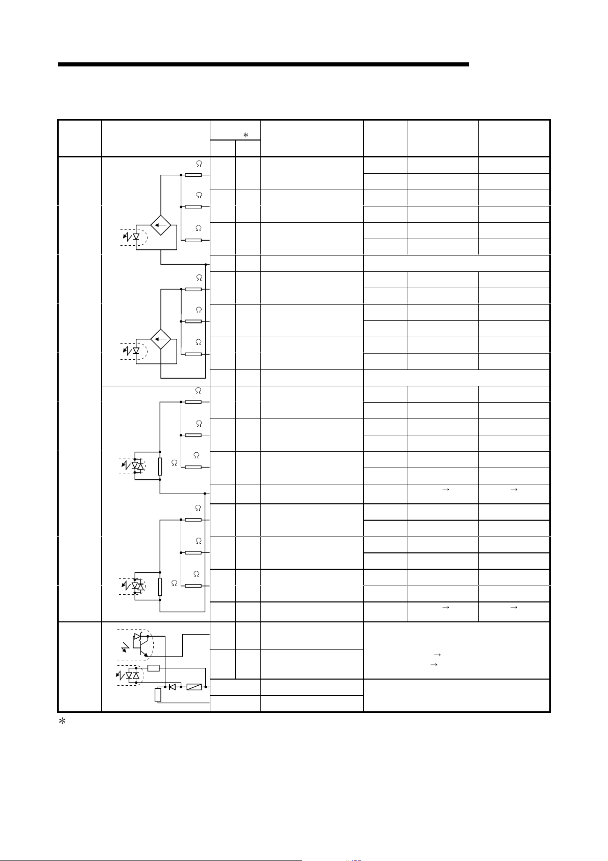
3.5 Interface with External Devices
The table below lists the external device interface for the QD62(E/D).
(1) QD62 (DC input sinking output type)
I/O
classification
Input
Output
Internal circuit
To the fuse
broken detection
circuit
1k
1/10W
1k
1/10W
4.7k
1/3W
3.3k
1/10W
470
1/16W
4.7k
1/3W
3.3k
1/10W
470
1/16W
10k
1/3W
5.6k
1/10W
2k
1/10W
10k
1/3W
5.6k
1/10W
2k
1/10W
FUSE
1: Terminal nu mbe rs A0 3, A04 , B03 an d B0 4 a re no t u sed .
Terminal
number
CH1 CH2
A20 A13 Phase A pulse input 24 V
B20 B13 Phase A pulse input 12 V
A19 A12 Phase A pulse input 5 V
B19 B12 ABCOM —
A18 A11 Phase B pulse input 24 V
B18 B11 Phase B pulse input 12 V
A17 A10 Phase B pulse input 5 V
—— — —
B17 B10 Preset input 24 V
A16 A09 Preset input 12 V
B16 B09 Preset input 5 V
A15 B08 CTRLCOM
B15 B08 Function start input 24 V
A14 A07 Function start input 12 V
B14 B07 Function start input 5 V
—— —
A06 A05
B06 B05
1
EQU1
(Coincidenc e ou tput poi nt No. 1)
EQU2
(Coincidenc e ou tput poi nt No. 2)
B02, B01 12/24 V
A02, A01 0 V
Signal name Operation
MELSEC-Q
Input voltage
(guaranteed va lu e)
When ON 21.6 to 26.4 V 2 to 5 mA
When OFF 5 V or less 0.1 mA or less
When ON 10.8 to 13.2 V 2 to 5 mA
When OFF 4 V or less 0.1 mA or less
When ON 4.5 to 5.5 V 2 to 5 mA
When OFF 2 V or less 0.1 mA or less
When ON 21.6 to 26.4 V 2 to 5 mA
When OFF 5 V or less 0.1 mA or less
When ON 10.8 to 13.2 V 2 to 5 mA
When OFF 4 V or less 0.1 mA or less
When ON 4.5 to 5.5 V 2 to 5 mA
When OFF 2 V or less 0.1 mA or less
When ON 21.6 to 26.4 V 2 to 5 mA
When OFF 5 V or less 0.1 mA or less
When ON 10.8 to 13.2 V 2 to 5 mA
When OFF 4 V or less 0.1 mA or less
When ON 4.5 to 5.5 V 2 to 5 mA
When OFF 2 V or less 0.1 mA or less
Response
time
When ON 21.6 to 26.4 V 2 to 5 mA
When OFF 5 V or less 0.1 mA or less
When ON 10.8 to 13.2 V 2 to 5 mA
When OFF 4 V or less 0.1 mA or less
When ON 4.5 to 5.5 V 2 to 5 mA
When OFF 2 V or less 0.1 mA or less
Response
time
Operating voltage 10.2 to 30 V
Maximum load current 0.5 A/point, 2 A/1 common
Maximum voltage drop when ON 1.5 V
Response ti me OFF
ON
Input voltage 10.2 to 30 V
Current consumption 8 mA (TYP 24 V DC)
ON
OFF
0.5 ms or less
ON
OFF
0.5 ms or less
ON 0.1 ms or less
OFF 0.1 ms or less (rated loa d,
Operating current
(guaranteed va lu e)
ON OFF
1 ms or less
ON OFF
1 ms or less
resistive load)
3 - 11 3 - 11
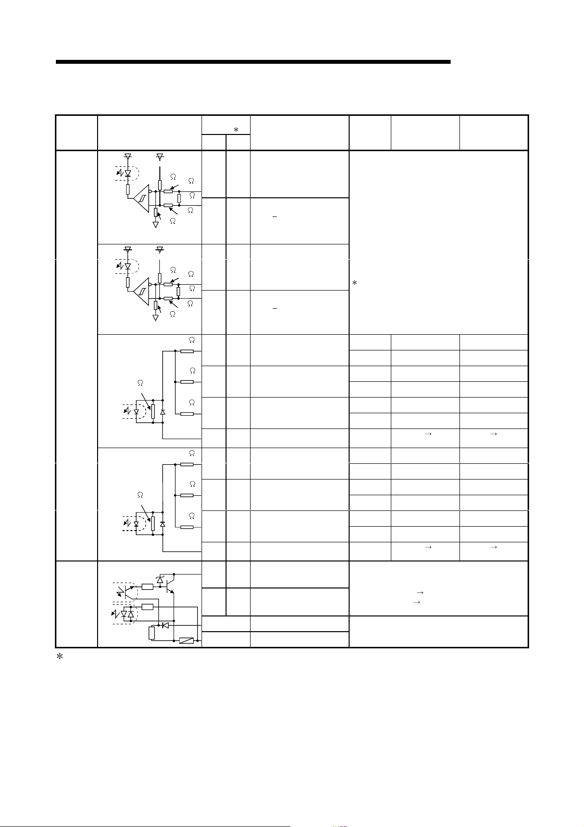
3 SPECIFICATIONS
(2) QD62E (DC input sourcing output type)
I/O
classification
Input
Internal circuit
1k
1/10W
1k
1/10W
4.7k
1/3W
3.3k
1/10W
470
1/16W
4.7k
1/3W
3.3k
1/10W
470
1/16W
10k
1/3W
5.6k
1/10W
2k
1/10W
10k
1/3W
5.6k
1/10W
2k
1/10W
Output
To the fuse
broken detection
circuit
FUSE
1: Terminal nu mbe rs A0 3, A04 , B03 an d B0 4 a re no t u sed .
Terminal
number
1
Signal name Operation
CH1 CH2
A20 A13 Phase A pulse input 24 V
B20 B13 Phase A pulse input 12 V
A19 A12 Phase A pulse input 5 V
B19 B12 ABCOM —
A18 A11 Phase B pulse input 24 V
B18 B11 Phase B pulse input 12 V
A17 A10 Phase B pulse input 5 V
—— — —
B17 B10 Preset input 24 V
A16 A09 Preset input 12 V
B16 B09 Preset input 5 V
A15 B08 CTRLCOM
B15 B08 Function start input 24 V
A14 A07 Function start input 12 V
B14 B07 Function start input 5 V
—— —
A06 A05
B06 B05
EQU1
(Coincidenc e ou tput poi nt No. 1)
EQU2
(Coincidenc e ou tput poi nt No. 2)
B02, B01 12/24 V
A02, A01 0 V
MELSEC-Q
Input voltage
(guaranteed va lu e)
When ON 21.6 to 26.4 V 2 to 5 mA
When OFF 5 V or less 0.1 mA or less
When ON 10.8 to 13.2 V 2 to 5 mA
When OFF 4 V or less 0.1 mA or less
When ON 4.5 to 5.5 V 2 to 5 mA
When OFF 2 V or less 0.1 mA or less
When ON 21.6 to 26.4 V 2 to 5 mA
When OFF 5 V or less 0.1 mA or less
When ON 10.8 to 13.2 V 2 to 5 mA
When OFF 4 V or less 0.1 mA or less
When ON 4.5 to 5.5 V 2 to 5 mA
When OFF 2 V or less 0.1 mA or less
When ON 21.6 to 26.4 V 2 to 5 mA
When OFF 5 V or less 0.1 mA or less
When ON 10.8 to 13.2 V 2 to 5 mA
When OFF 4 V or less 0.1 mA or less
When ON 4.5 to 5.5 V 2 to 5 mA
When OFF 2 V or less 0.1 mA or less
Response
time
ON
OFF
0.5 ms or less
When ON 21.6 to 26.4 V 2 to 5 mA
When OFF 5 V or less 0.1 mA or less
When ON 10.8 to 13.2 V 2 to 5 mA
When OFF 4 V or less 0.1 mA or less
When ON 4.5 to 5.5 V 2 to 5 mA
When OFF 2 V or less 0.1 mA or less
Response
time
ON
OFF
0.5 ms or less
Operating voltage 10.2 to 30 V
Maximum load current 0.1 A/point, 0.4 A/1 common
Maximum voltage drop when ON 1.5 V
Response ti me OFF
ON 0.3 ms or less
ON
OFF 0.3 ms or less (rated loa d,
Input voltage 10.2 to 30 V
Current consumption 8 mA (TYP 24 V DC)
Operating current
(guaranteed va lu e)
ON OFF
1 ms or less
ON OFF
1 ms or less
resistive load)
3 - 12 3 - 12
3 SPECIFICATIONS
(3) QD62D (Differential input sinking output type)
I/O
classification
Internal circuit
+ 5V
(DC/DC converter)
Line
receiver
1/16W
+ 5V
(DC/DC converter)
Line
receiver
1/16W
27k
1/16W
27k
27k
1/16W
27k
Terminal
number
1
CH1 CH2
A20 A14 Phase A pulse input
4.7k
1/16W
100
1/2W
4.7k
1/16W
B20 B14 Phase A pulse input
A19 A13 Phase B pulse input
4.7k
1/16W
100
1/2W
4.7k
1/16W
A19 B13 Phase B pulse input
Signal name Operation
Line driver lev e l (A m26L S31 [ manu fa c tur ed by Texa s
Instruments ] or equ iva le nt ) th at co nf or ms to RS- 422 - A in
EIA Standard
EIA standard R S-42 2- A line dri ver l ev e l
Equivalent to Am26LS31 (made by Japan Texas
Instruments, Inc.)
V
Hysteresis (VT+ - VT-) 60 mV
hys
V
"H" level enable in put vo l ta ge : 2 V or high er
IH(E)
V
"L" level enable input voltage: 0.8 V or lower
IL(E)
A current type li ne drive r ca nn ot be us e d.
Input voltage
(guaranteed va lu e)
MELSEC-Q
Operating current
(guaranteed va lu e)
Input
Output
1k
1/10W
1k
1/10W
To the fuse
broken detection
circuit
10k
1/3W
A18 A12 Preset input 24 V
5.6k
1/10W
B18 B12 Preset input 12 V
680
1/10W
A17 A11 Preset input 5 V
B17 B11 PRSTCOM
10k
1/3W
A16 A10 Function start input 24 V
5.6k
1/10W
B16 B10 Function start input 12 V
680
1/10W
A15 A09 Function start input 5 V
B15 B09 FUNCCOM
A06 A05
B06 B05
EQU1
(Coincidenc e ou tput poi nt No. 1)
EQU2
(Coincidenc e ou tput poi nt No. 2)
B02, B01 12/24 V
FUSE
A02, A01 0 V
When ON 21.6 to 26.4 V 2 to 5 mA
When OFF 5 V or less 0.1 mA or less
When ON 10.8 to 13.2 V 2 to 5 mA
When OFF 4 V or less 0.1 mA or less
When ON 2.5 to 5.5 V 2 to 5 mA
When OFF 1 V or less 0.1 mA or less
Response
time
ON
OFF
0.5 ms or less
ON OFF
1 ms or less
When ON 21.6 to 26.4 V 2 to 5 mA
When OFF 5 V or less 0.1 mA or less
When ON 10.8 to 13.2 V 2 to 5 mA
When OFF 4 V or less 0.1 mA or less
When ON 2.5 to 5.5 V 2 to 5 mA
When OFF 1 V or less 0.1 mA or less
Response
time
ON
OFF
0.5 ms or less
ON OFF
1 ms or less
Operating voltage 10.2 to 30 V
Maximum load current 0.5 A/point, 2 A/1 common
Maximum voltage drop when ON 1.5 V
Response ti me OFF
ON 0.1 ms or less
OFF 0.1 ms or less (rated loa d,
ON
resistive load)
Input voltage 10.2 to 30 V
Current consumption 8 mA (TYP 24 V DC)
1: Terminal numbers A08, A07, A03, A04, B08, B07, B04 and B03 are not used.
3 - 13 3 - 13

3 SPECIFICATIONS
3.6 Encoders that can be Connected
The encoders that can be connected to the QD62(E/D) are described below.
(1) Encoders that can be connected to the QD62 and QD 62E
• Open collector ou tp ut ty pe en co de rs
• CMOS level voltage output type encoders
(Verify that the encoder output voltage meets the specifications for the QD62
and QD62E.)
(2) Encoders that can be connected to the QD62D
• Line driver output type encoders
(Verify that the encoder output voltage meets the specifications for the
QD62D.)
POINT
The following encoders cannot be used with the QD62(E/D).
• TTL level voltage output type encoders
MELSEC-Q
3 - 14 3 - 14
 Loading...