

Page 1

<Dual-In-Line Package Intelligent Power Module >
DIPIPM+ Series APPLICATION NOTE
PSSxxMC1Fx, PSSxxNC1Fx
Table of contents
CHAPTER 1 : INTRODUCTI ON ............................................................................................................................... 2
1.1 Feature of DIPIPM+ ..................................................................................................................................................................................... 2
1.2 Functions ..................................................................................................................................................................................................... 3
1.3 Applications ................................................................................................................................................................................................. 3
1.4 Line-up ........................................................................................................................................................................................................ 4
CHAPTER 2 : SPE CI FICATIONS and CHARACTERISTICS ................................................................................. 5
2.1 Specification of DIPIPM+ ............................................................................................................................................................................. 5
2.1.1 Maximum ratings ........................................................................................................................................................................................................................... 5
2.1.2 Thermal Resistance ...................................................................................................................................................................................................................... 8
2.1.3 Electric Characteristics and Recommended Conditions ............................................................................................................................................................... 9
2.1.4 Mechanical characteristics and speci fications ............................................................................................................................................................................13
2.2 Protection functions and operating sequence ............................................................................................................................................ 14
2.2.1 Short circ uit pr otection.................................................................................................................................................................................................................14
2.2.2 Control Supply UV Protection .....................................................................................................................................................................................................16
2.2.3 Temperature output function VOT ................................................................................................................................................................................................19
2.3 Package outline of DIPIPM+ ...................................................................................................................................................................... 21
2.3.1 Package outline ...........................................................................................................................................................................................................................21
2.3.2 Marking ........................................................................................................................................................................................................................................22
2.3.3 Terminal Description ...................................................................................................................................................................................................................23
2.4 Mounting Method ....................................................................................................................................................................................... 26
2.4.1 Electric Spacing of DIPIPM+ .......................................................................................................................................................................................................26
2.4.2 Mounting Method and Precautions .............................................................................................................................................................................................26
2.4.3 Soldering Conditions ...................................................................................................................................................................................................................28
CHAPTER 3 : SYSTEM APPL ICATION G UIDANCE ............................................................................................ 29
3.1 Application guidance ................................................................................................................................................................................. 29
3.1.1 System connection ......................................................................................................................................................................................................................29
3.1.2 Interface Circuit (Direct Coupling Interface example for using one shunt resistor) ....................................................................................................................30
3.1.3 Interface circuit (example of opto-coupler isolated interface) .....................................................................................................................................................32
3.1.4 External SC protection circuit with using three shunt resistors...................................................................................................................................................33
3.1.5 Circuits of Signal Input Terminals and Fo Terminal ....................................................................................................................................................................33
3.1.6 Snubber circuit ............................................................................................................................................................................................................................35
3.1.7 Recommen de d wiri ng me tho d a rou nd s hu nt resistor .................................................................................................................................................................36
3.1.8 SOA of DIPIPM+ at switching state ............................................................................................................................................................................................38
3.1.9 SCSOA ........................................................................................................................................................................................................................................39
3.1.10 Power Life Cycles ......................................................................................................................................................................................................................40
3.2 Power loss and thermal dissipation calculation .......................................................................................................................................... 41
3.2.1 Power loss calculation .................................................................................................................................................................................................................41
3.2.2 DIPIPM+ performance according to carreir frequency ...............................................................................................................................................................43
3.3 Noise and ESD withstand capability........................................................................................................................................................... 45
3.3.1 Evaluation circuit of noise withstand capability ...........................................................................................................................................................................45
3.3.2 Countermeasures and precautions .............................................................................................................................................................................................46
3.3.3 Static electricity withstand capability ...........................................................................................................................................................................................47
CHAPTER 4 : Bootstrap Circuit O peration ......................................................................................................... 48
4.1 Bootstrap Circuit Operation ........................................................................................................................................................................ 48
4.2 Bootstrap supply circuit current at switching state ...................................................................................................................................... 49
4.3 Note for designing the bootstrap circuit ...................................................................................................................................................... 51
4.4 Initi a l charging in bootstrap circuit .............................................................................................................................................................. 52
CHAPTER 5 : PACKAGE HANDLING .................................................................................................................. 53
5.1 Packaging Specification ............................................................................................................................................................................. 53
5.2 Handling Precautions................................................................................................................................................................................. 54
Publication Date: September 2016
1
Page 2
< Dual-In-Line Package Intelligent Power Module >
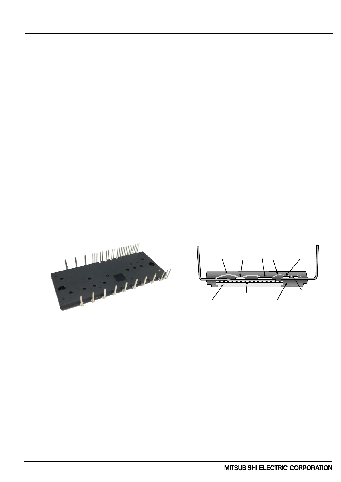
Fig.1-1. Package photograph
1-2 Cross-sectional structure
Molding resin
Aluminum heatsink
Insulation sheet
IGBT
IC
FWDi
Aluminum wire
Gold wire
Copper frame
BSD
DIPIPM+ Series Application note
CHAPTER 1 : INTRODUCTION
1.1 Feature of DIPIPM+ DIPIPM+ series is our latest transfer molding CIB type IPM(CIB: Converter Inverter Brake, IPM: Intelligent
Power Module). It in tegrates the inverter, c onverter and brake parts to make up a compact inverter systems for
commercial and industria l inverter application lik e com m ercial air c ondi tioner, ser vo an d gener al purpose inverter.
We also offers DIPIPM+ without brake type.
General DIPIPM integrates a inverter part only, but recent market demand requires highly integrated IPM
products including more functions and peripheral circuits. So we realized this All-in-One DIPIPM, “DIPIPM+”.
DIPIPM+ series is well designed transfer molding package from our long term histroy as the pioneer.
DIPIPM+ integrates m ain compornents f or inverter circuit a nd it will contribute to reduce total cos t by smaller
mounting area for inverter circuit, shorter designing time and more reasonable assembly cost. It employs
low-voltage (LV) and high voltage (HV) control ICs a nd their correspon ding bootstrap circ uit for IGBT driving and
protection, as same as general DIPIPM series. So DIPIPM+ series enable same system design for its inverter part
like general DIPIPM series.
By adopting same s tructur e of heat r adiation as Lar ge DIPIPM ser ies which h as h igh th erm al conduc tivit y, it is
possible to design system with high reliability.
Main features of this series are described as follows;
・
Newly optimized CSTBT are integrated for improving performance
・
1200V series covers from 5A to 35A and 600V has 50A rating product, DIPIPM+ has wide lineup
・
Easy to design a PCB pattern wiring by smart terminal layout.
・
Incorporating bootstrap diode(BSD) with current limiting resistor for P-side gate driving supply
・
Easy to use temperature output function of the sensor integrated on control IC
Fig.1-1 shows package photograph and Fig.1-2 shows the cross-sectional structure.
Publication Date: September 2016
図
2
Page 3
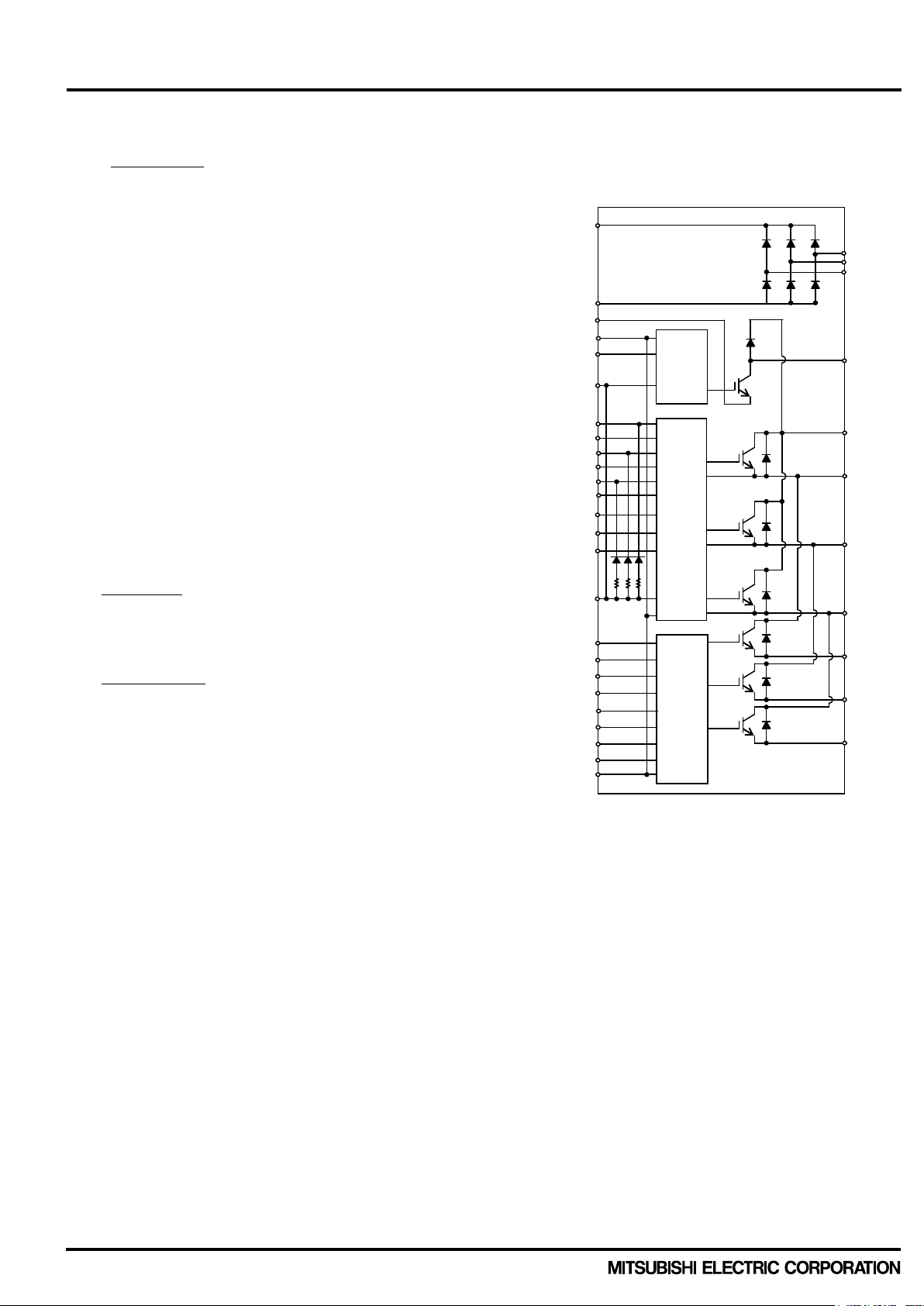
< Dual-In-Line Package Intelligent Power Module >
Inverter block
Fig. 1-3 Internal circuit block diagram for
DIPIPM+ with Brake circuit
UN
VN
WN
Fo
VN1
V
VFB
VP
V
WFB
WP
UP
VNC
CIN P U
V W NW
VP1
LVIC
V
UFB
NV
NU
VOT
HVIC
P1 R S
T
N1
B
N(B)
AIN
VNC
LVIC
VP1
V
V
VFS
V
WFS
CFo
DIPIPM+ Series Application note
1.2 Functions
Brake block
Common items
●For P-side IGBT
- Drive circuit
- High voltage level shift circuit
- Control supply under voltage (UV)
lockout circuit (without fault signal output)
- Built-in bootstrap diode (BSD)
with current limiting resistor
●For N-side IGBTs:
- Drive circuit;
- Short circuit (SC) protection circuit
- Control supply under voltage (UV)
lockout circuit (with fault signal output)
- Outputting LVIC temperature by analog signal
(No self over temperature protection)
(note) about SC protection
By detecting voltage of external shunt resistor,
DIPIPM+ works to protect.
●Fault signal output
- Corresponding to N-side IGBT SC protection
and N-side UV protection.
●For IGBT
- Drive circuit
- UV protection circuit without fault signal
●IGBT drive supply
- Single DC15V power supply
●Control input supply
- High active logic with 5V
●UL recognized
- UL1557 File E323585
UFS
1.3 Applications
Motor drives for low power industrial equipment and commercial equipment such as air conditioners
Publication Date: September 2016
3
Page 4

< Dual-In-Line Package Intelligent Power Module >
Type name
Rated current
Rated voltage
Motor ratings
(note1)
Brake
Isolation voltage
PSS05MC1FT
5A
0.75kW/440VAC
PSS10MC1FT
10A
1.5kW/440VAC
PSS15MC1FT
15A
2.2kW/440VAC
PSS25MC1FT
25A
3.7kW/440VAC
PSS35MC1FT
35A
5.5kW/440VAC
PSS50MC1F6
50A
600V
3.7kW/220VAC
Type name
Rated current
Rated voltage
Motor ratings
(note1)
Brake
Isolation voltage
PSS05NC1FT
5A
0.75kW/440VAC
PSS10NC1FT
10A
1.5kW/440VAC
PSS15NC1FT
15A
2.2kW/440VAC
PSS25NC1FT
25A
3.7kW/440VAC
PSS35NC1FT
35A
5.5kW/440VAC
PSS50NC1F6
50A
600V
3.7kW/220VAC
DIPIPM+ Series Application note
1.4 Line-up
Line-ups are described as following table 1-1. and 1-2.
Table 1-1. DIPIPM+ with Brake circuit
1200V
Yes 2500Vrms
Table 1-1. DIPIPM+ without Brake circuit
1200V
No 2500Vrms
(note 1)
The motor ratings are described for industrial and general motor capability, and actual ratings are different
with application condition.
(note 2)
Isolation voltage is tested under the condition of which all terminals are connected with conductive
material and DIPIPM+ is applied 60Hz sinusoidal voltage between the terminals and heatsink for 1minute.
(note2)
(note2)
Publication Date: September 2016
4
Page 5
< Dual-In-Line Package Intelligent Power Module >
INVERTER PART
Symbol Parameter Condition
Ratings
Unit
V
CC
Supply voltage
Applied between P-NU,NV,NW
900
V
V
CC(surge)
Supply voltage (surge)
Applied between P-NU,NV,NW
1000
V
V
CES
Collector-emitter voltage
1200
V
±IC
Each IGBT collector current
TC= 25°C
(Note 1)
25
A
±ICP
Each IGBT collector current (peak)
TC= 25°C, less than 1ms
50
A
Tj
Junction temperature
-30~+150
°C
BRAKE PART
Symbol Parameter Condition
Ratings
Unit
V
Supply voltage
Applied between P-N(B)
900
V
V
CC(surge)
Supply voltage (surge)
Applied between P-N(B)
1000
V
V
CES
Collector-emitter voltage
1200
V
IC
Each IGBT collector current
TC= 25°C
15
A
ICP
Each IGBT collector current (peak)
TC= 25°C, less than 1ms
30
A
V
RRM
Repetitive peak reverse voltage
1200
V
IF
Forward current
TC= 25°C
15
A
CONVERTER PART
Symbol Parameter Condition
Ratings
Unit
Repetitive peak reverse voltage
Io
DC output current
3-phase full wave rectification
25
A
I
FSM
Surge forward current
Peak value of half cycle at 60Hz, Non-repetitive
315
A
I2t
I2t capability
Value for 1 cycle of surge current
416
A2s
Tj
Junction temperature
-30~+150
°C
CONTROL (PROTECTION) PART
Symbol Parameter Condition
Ratings
Unit
VD
Control supply voltage
Applied between
VP1-VNC, VN1-VNC
20
V
VDB
Control supply voltage
Applied between
V
, V
, V
20
V
VIN
Input voltage
Applied between
UP,VP,WP,UN, VN, WN, AIN-VNC
-0.5~VD+0.5
V
F
VSC
Current sensing input voltage
Applied between CIN-VNC
-0.5~VD+0.5
V
(1)
(2)
(3)
(4)
(5)
(5)
(5)
DIPIPM+ Series Application note
CHAPTER 2 : SPECIFICATIONS and CHARACTERISTICS
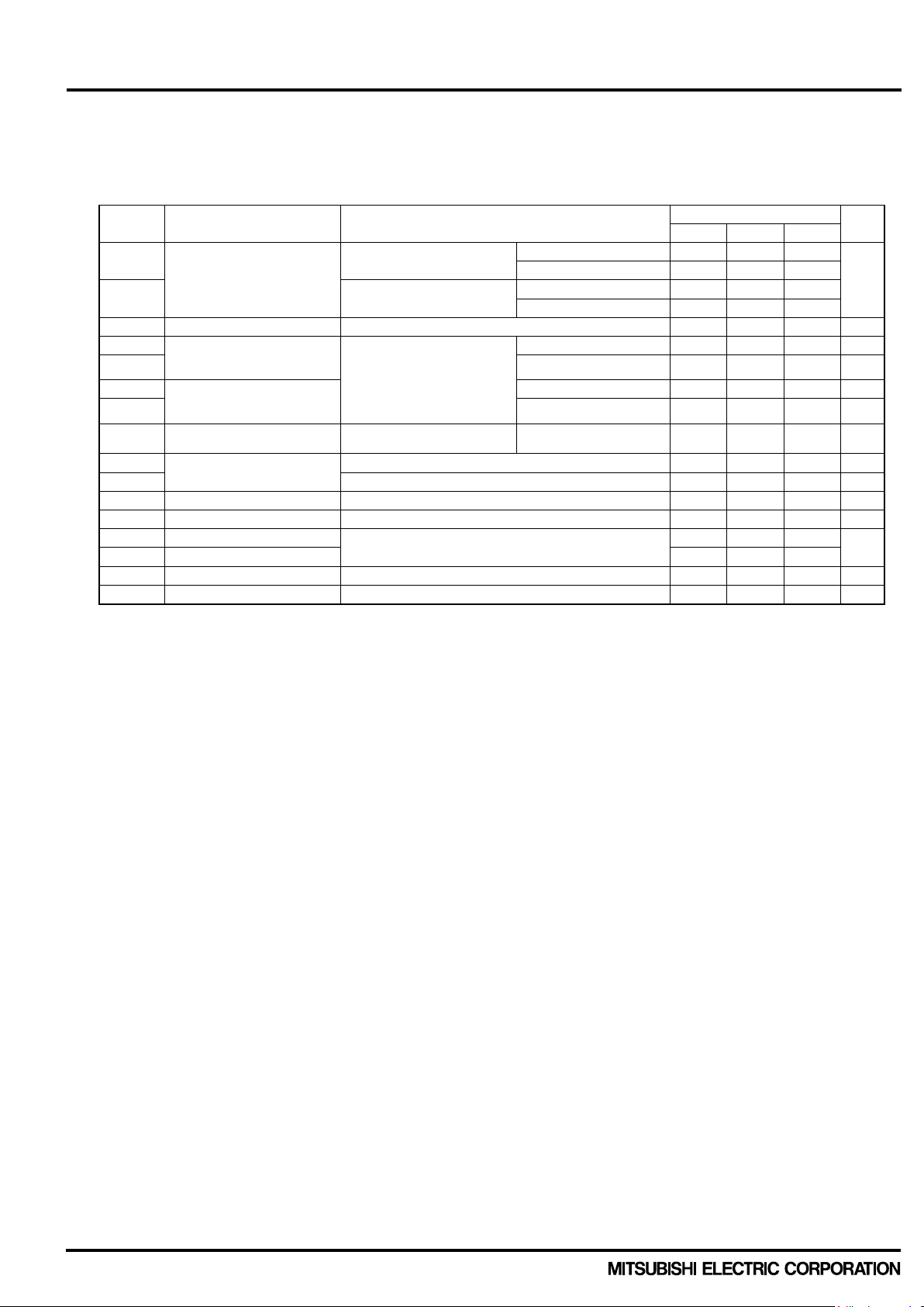
2.1 Specification of DIPIPM+ It is representatively described as follows with PSS25MC1FT (25A/1200V,CIB type). For the other products, please refer each data sheets in details.
2.1.1 Maximum ratings Maximum ratings are described as following table 2-1-1. (T
Table 2-1-1 Maximum rating of PSS25MC1FT (25A/1200V,CIB type)
MAXIMUM RATINGS (T
= 25°C, unless otherwise noted)
j
= 25°C, unless otherwise noted)
j
CC
IFP Forward current (peak) 30 A
Tj Junction temperature -30~+150 °C
V
RRM
1600 V
(Note 1)
VFO Fault output supply voltage Applied between
IFO Fault output current Sink current at FO terminal 5 mA
Note1: Pulse width and period are limited due to junction temperature.
Publication Date: September 2016
UFB-VUFS
O-VNC
5
VFB-VVFS
-0.5~VD+0.5 V
WFB-VWFS
Page 6
< Dual-In-Line Package Intelligent Power Module >
TOTAL SYSTEM
Symbol Parameter Condition
Ratings
Unit
Self protection supply voltage limit
(Short circuit protection capability)
VD = 13.5~16.5V, Inverter Part
Tj = 125°C, non-repetitive, less than 2μs
TC
Module case operation temperature
-30~+110
°C
T
stg
Storage temperature
-40~+125
°C
60Hz, Sinusoidal, AC 1min, between connected all
pins and heat sink plate
No.
Symbol
Description
brake circuit is necessary if P-N voltage exceeds this value.
The maximum P-N surge voltage in switching status. If P-N voltage exceeds this voltage, a
snubber circuit is necessary to absorb the surge under this voltage.
(3)
V
CES
The maximum sustained collector-emitter voltage of built-in IGBT and FWDi.
are limited due to junction temperature.
The maximum junction temperature rating is 150°C. But for safe operation, it is recommended
for safety design.
The maximum supply voltage for turning off IGBT s afely in the case of an SC or OC faults.
higher than this specif ic atio n.
Isolation voltage is the withstanding voltage between all terminals connected with conductive
material and heatsink of heat radiation.
information. Due to the control schemes such different control between P and
is necessary to change the measuring point to that under the highest power chip.
Tc point
IGBT chip
Heat radiation
6.4mm
19.6mm
Control terminals
Power terminals
(7)
(6)
DIPIPM+ Series Application note
V
CC(PROT)
V
Isolation voltage
iso
Note2: Measurement point of Tc is described in below figure. (8)
(Note 2)
800 V
2500 V
rms
surface
(1) VCC
(2) V
CC(surge)
(4) +/- IC
(5) Tj
(6) V
CC(PROT)
(7) Viso
(8) Tc position
The maximum voltage can be biased between P-N. A voltage suppressing circuit such as a
The allowable cont inuous current flowing at collect electrode (Tc=25°C) Pulse width and period
to limit the average junction temperature up to 125°C (at Tc is less than 100℃). Repetitive
temperature variation ΔTj affects the life time of power cycle, so please refer life time curves
The power chip might not be protected and break down in the case that the supply voltage is
Tc (case temperature) is defined to be the temperature just beneath the specified power chip.
Please mount a thermocouple on the heat sink surface at the defined position to get accurate
temperature
N-side, there is the possibility that highest Tc point is different from above point. In such cases, it
Publication Date: September 2016
6
Page 7
< Dual-In-Line Package Intelligent Power Module >
INV-IGBT x 6
INV-Di x 6
Br UP VP WP UN VN WN
Br-Di
CONV-Di x 3
CONV-Di x 3
RP SP TP
RN SN TN
Tc position
Br-IGBT
Reference point of
location
DIPIPM+ Series Application note
Power chips layout
Fig.2-1-1 indicates the position of the each power chips. (This figure is the view from laser marked side.)
In case of PSSxxNC1Fx, Br-IGBT and Br-Di are not built-in.
Fig. 2-1-1 Power chips layout (Unit : mm)
Publication Date: September 2016
7
Page 8
< Dual-In-Line Package Intelligent Power Module >
Limits
Min.
Typ.
Max.
R
Inverter IGBT part (per 1/6 module)
- - 1.15
R
th(j-c)F
Inverter FWD part (per 1/6 module)
- - 1.65
R
th(j-c)Q
Brake IGBT part (per 1module)
- - 1.45
R
Brake Di part (per 1module)
- - 1.65
R
Converter part (per 1/6module)
- - 1.10
0.01
0.10
1.00
0.001 0.01 0.1 1
Normalized transient
thermal impedance Zth(j-c)*
DIPIPM+ Series Application note
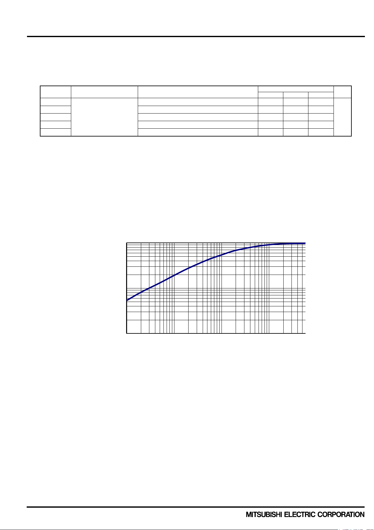
2.1.2 Thermal Resistance Table 2-1-2 shows the thermal resistance between its chip junction and case.
Table 2-1-2. Thermal resistance of PSS25MC1FT (25A/1200V, CIB type)
Symbol Parameter Condition
th(j-c)Q
Junction to case thermal
th(j-c)F
resistance
th(j-c)R
(Note 3)
Unit
K/W
Note 3: Grease with good thermal conductivity and long-term endurance should be applied evenly with about +100μm~
+200μm on the contacting surface of DIPIPM and heat sink. The contacting thermal resistance between DIPIPM
case and heat sink Rth(c-f) is determined by the thickness and the thermal conductivity of the applied grease.
For reference, Rth(c-f) is about 0.25K/ W (per 1chip, grease thickness: 20μm, thermal conductivity: 1.0W/m•K).
The above data shows static state ther m al resis tance. T he ther m al resistanc e goes into sat uratio n in about 10
seconds. The unsaturated thermal resistance is called as transient thermal impedance which is shown in
Fig.2-1-2. Zth(j-c)* is the normalized transient thermal impedance and formulation is described as Zth(j-c)*=
Zth(j-c) / Rth(j-c)max. For example, the IGBT transient thermal impedance at 0.2s is 1.15×0.7=0.81K/W. The
transient thermal im pedance isn’t used for constantly current, but f or short period current as millisecond order.
(e.g. motor starting, motor lock・・・e.t.c)
Publication Date: September 2016
Fig. 2-1-2. Normalized transient thermal impedance
8
Page 9
< Dual-In-Line Package Intelligent Power Module >
INVERTER PART
IC= 25A, Tj= 25°C
-
1.50
2.20
IC= 25A, Tj= 125°C
-
1.80
2.45
VEC
FWDi forward voltage
VIN= 0V, -IC= 25A
-
2.40
3.10
V
ton
1.10
1.90
2.60
μs
t
C(on)
- 0.60
0.90
μs
t
off
- 2.80
3.80
μs t
C(off)
- 0.50
0.90
μs
trr - 0.60 - μs
Tj= 25°C
- - 1
Tj= 125°C
- - 10
BRAKE PART
IC= 15A, Tj= 25°C
-
1.50
2.20
IC= 15A, Tj= 125°C
-
1.80
2.45
VF
Di forward voltage
VIN= 0V, IF= 15A
-
2.20
2.80
V
ton
1.10
1.90
2.60
μs t
C(on)
- 0.65
1.00
μs t
off
- 2.60
3.60
μs
t
C(off)
- 0.40
0.95
μs
trr - 0.65 - μs
Tj= 25°C
- - 1
Tj= 125°C
- - 10
CONVERTER PART
Limits
Repetitive reverse current
−
Forward voltage drop
DIPIPM+ Series Application note
2.1.3 Electric Characteristics and Recommended Conditions Table 2-1-3 shows the typical static characteristics and switching characteristics. (T
Table 2-1-3 Static characteristics and switching characteristics of PSS25MC1FT(25A/1200V, CIB type)
ELECTRICAL CHARACTERISTICS (T
= 25°C, unless otherwise noted)
j
= 25°C, unless otherwise noted)
j
Symbol Parameter Condition
V
CE(sat)
Collector-emitter saturation
voltage
Switching times
VD=VDB = 15V, VIN= 5V
V
= 600V, VD= VDB= 15V
CC
= 25A, Tj= 125°C, VIN= 0↔ 5V
I
C
Inductive Load (upper-lower arm)
I
CES
Collector-emitter cut-off
current
VCE=V
CES
Symbol Parameter Condition
V
I
CES
CE(sat)
Collector-emitter saturation
voltage
Switching times
Collector-emitter cut-off
current
VD=VDB = 15V, VIN= 5V
V
= 600V, VD= VDB= 15V
CC
= 15A, Tj= 125°C, VIN= 0↔ 5V, Inductive Load
I
C
VCE=V
CES
Limits
Min. Typ. Max.
Limits
Min. Typ. Max.
Unit
V
mA
Unit
V
mA
Symbol Parameter Condition
I
RRM
VF
VR=V
IF=25A
, Tj=125°C
RRM
Min. Typ. Max.
−
−
1.1 1.4
7.0
Unit
mA
V
Publication Date: September 2016
9
Page 10
< Dual-In-Line Package Intelligent Power Module >
trr
Irr
tc(on)
10%
10%
10%
10%
90%
90%
td(on)
tc(off)
td(off)
tf
tr
( ton=td(on)+tr )
( toff=td(off)+tf )
Ic
VCE
V
CIN
P-side SW
Input signal
N-side SW
Input signal
VIN(5V⇔0V)
VD
VCC
IN GND CIN
LO
VCC
IN
VB
S
HO
UP,VP,WP
UN,VN,WN
VNC
V
UFB,VVFB,VWFB
VN1
CIN
COM
VP1 P U,V,W
Ic
VCC
N-side
P-side
VDB
NU,NV,
NW
V
UFS,VVFS,VWFS
L load
L load
time:500nsec/div.
VCE:200V/div.
Ic:10A/div.
time:500nsec/div.
VCE:200V/div.
Ic:10A/div.
DIPIPM+ Series Application note
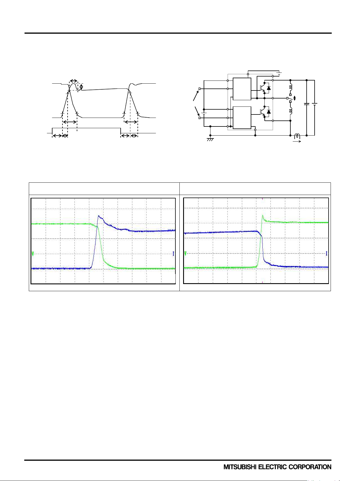
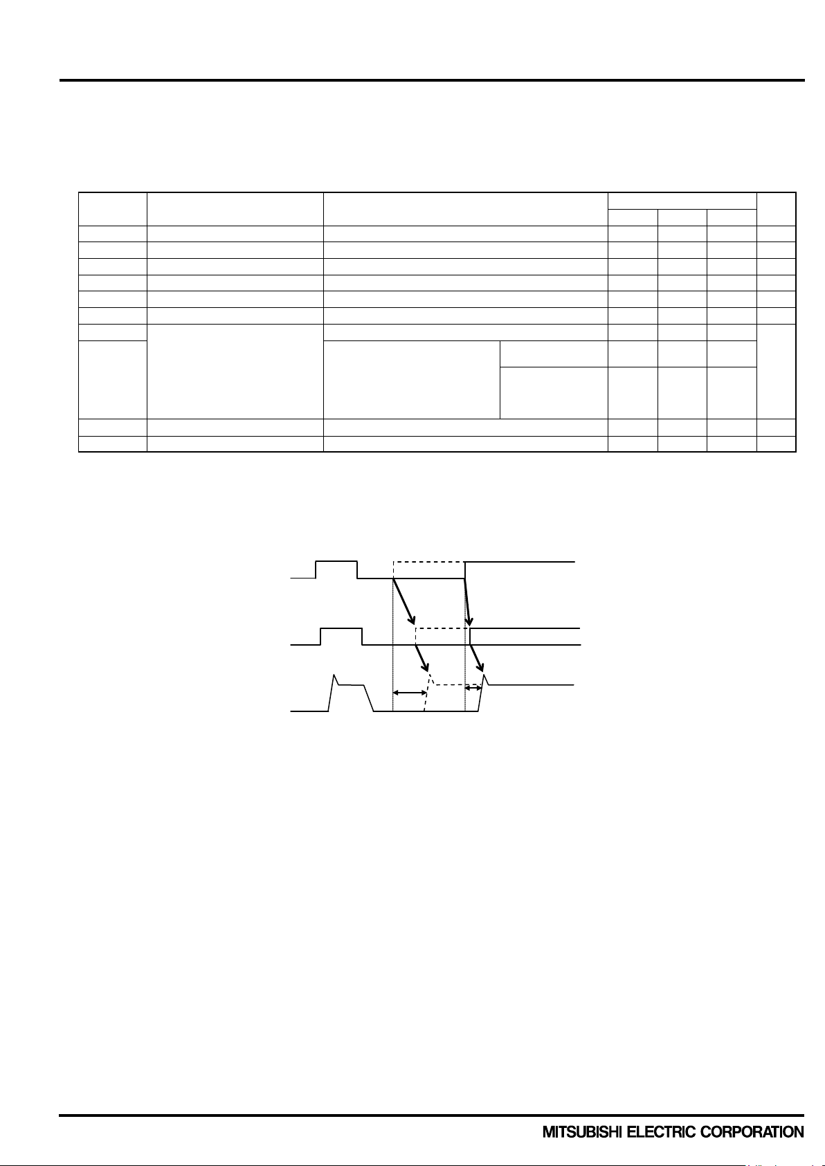
Definition of switching time and performance test topology are shown in Fig.2-1-3 and 2-1-4.
Switching characteristics are measured b y half bridge c irc uit with ind uct ance loa d.
Fig. 2-1-3 Switching time definition Fig. 2-1-4 Evaluation circuit (inductive load)
V
TURN OFF TURN ON
Fig. 2-1-5 Typical switching waveform for PSS25MC1FT (25A/1200V) inverter part
Condition: V
=600V, VD=VDB=15V, Ic=25A, Tj=125°C, inductive load half bridge circuit
CC
Publication Date: September 2016
10
Page 11
< Dual-In-Line Package Intelligent Power Module >
CONTROL (PROTECTION) PART
Min.
Typ.
Max.
VD=15V, VIN=0V
- - 5.70
VD=15V, VIN=5V
- - 5.70
V
SC(ref)
Short circuit trip level
VD = 15V
0.455
0.480
0.505
V
UV
DBt
Control supply under-voltage
inverter part
Trip level
10.0 - 12.0
V
UVDt
Control supply under-voltage
inverter part and brake part
Trip level
10.3 - 12.5
V
LVIC
Temperature=100°C
tFO
Fault output pulse width
In case of CFo=22nF
1.6
2.4
ms
IIN
Input current
VIN = 5V
0.70
1.00
1.50
mA
V
th(on)
ON threshold voltage
-
3.5
V
th(off)
OFF threshold voltage
0.8
-
VF
Bootstrap Di forward voltage
IF=10mA including voltage drop by limiting resistor
0.9
1.3
V R Built-in limiting resistance
Included in bootstrap Di
16
20
24
Ω
DIPIPM+ Series Application note
Table 2-1-4 shows the typical control part characteristics. (T
Table 2-1-4. Typical control part characteristics of PSS25MC1FT(25A/1200V, CIB type)
= 25°C, unless otherwise noted)
j
Symbol Parameter Condition
ID
Circuit current
IDB
UV
UVDr Reset level 10.8 - 13.0 V
VOT Temperature Output Pull down R=5.1kΩ (Note 5)
V
FOH
V
FOL
protection(UV) for P-side of
Reset level 10.5 - 12.5 V
DBr
protection(UV) for N-side of
Fault output voltage
VSC = 1V, IFO = 1mA - - 0.95 V
Total of VP1-VNC, VN1-VNC
=15V, VIN=0V - - 0.55
V
Each part of V
V
VSC = 0V, FO terminal pulled up to 5V by 10kΩ 4.9 - - V
Applied between UP,VP,WP,UN, VN, WN, AIN-VNC
VFB-VVFS
, V
WFB-VWFS
UFB-VUFS
,
D=VDB
VD=VDB=15V, VIN=5V - - 0.55
(Note 4)
2.89 3.02 3.14 V
(Note 6,7)
-
Limits
-
-
Note 4 : SC protection works only for N-side IGBT in inverter part. Please select the external shunt resistance such that
the SC trip-level is less than 1.7 times of the current rating.
5 : DIPIPM don't shutdown IGBTs and output fault signal automatically when temperature rises excessively. When
temperature exceeds the protective level that user defined, controller (MCU) should stop the DIPIPM.
Temperature of LVIC vs. VOT output characteristics is described in Section 2.2.3.
6 : Fault signal Fo outputs when SC or UV protection works for N-side IGBT in inverter part. The fault output
pulse-width t
is depended on the capacitance value of CFO (CFO = tFO × 9.1 × 10⁻⁶ [F]).
FO
7 : UV protection also works for P-side IGBT in inverter part or brake part without fault signal Fo.
Unit
mA
V
Publication Date: September 2016
11
Page 12
< Dual-In-Line Package Intelligent Power Module >
RECOMMENDED OPERATION CONDITIONS
Limits
Min.
Typ.
Max.
VCC
Supply voltage
Applied between P-NU,NV,NW
0
600
800
V
VD
Control supply voltage
Applied between VP1-VNC,VN1-VNC
13.5
15.0
16.5
V
t
dead
Arm shoot-through blocking time
For each input signal
3.0 - -
μs
f
PWM
PWM input frequency
T
C
100°C, T
j
125°C
- - 20
kHz
PWIN(on)
1.5 - -
Less than
rated current
From rated
current
VNC
VNC variation
Between VNC- NU、NV、NW (including surge)
-5.0 - +5.0
V
Tj
Junction temperature
-20 - 125
°C
P Side Control Input
Internal IGBT Gate
Output Current Ic
t1
t2
Real line…off pulse width>PWIN(off); turn on time t1
Broken line
DIPIPM+ Series Application note
Table 2-1-5 shows recommended operation conditions. Please apply and use under the recommended conditions
to operate DIPIPM+ series safely. (T
Table 2-1-5. Recommended operation conditions of PSS25MC1FT (25A/1200V, CIB type)
= 25°C, unless otherwise noted)
j
Symbol Parameter Condition
VDB Control supply voltage Applied between V
ΔVD, ΔVDB Control supply variation -1 - 1 V/μs
≤
I
≤1.7 times of rated current (Note 8)
C
≤800V, 13.5≤VD≤16.5V,
0≤V
PWIN(off)
Note 8: DIPIPM might not make response if the input signal pulse width is less than PWIN(on).
Minimum input pulse width
CC
13.0≤V
N line wiring inductance
less than 10nH
≤18.5V, -20≤TC≤100°C,
DB
UFB-VUFS,VVFB-VVFS,VWFB-VWFS
≤
(Note 9)
current to 1.7
times of rated
13.0 15.0 18.5 V
3.0 - -
3.5 - -
9: DIPIPM might make no response or delayed response (P-side IGBT only) for the input signal with off pulse width
less than PWIN(off). Please refer below figure about delayed response.
About Delayed Response Against Shorter Input Off Signal Than PWIN(off) (P side only)
…off pulse width<PWIN(off); turn on time t2
[note] About control supply variation
If high frequency noise superimposed to the control supply line, IC malfunction might happen and cause DIPIPM erroneous
operation. To avoid such problem, line ripple voltage should meet the following specifications:
dV/dt ≤ +/-1V/μs, Vripple≤2Vp-p
Unit
μs
Publication Date: September 2016
12
Page 13
< Dual-In-Line Package Intelligent Power Module >
MECHANICAL CHARACTERISTICS AND RATINGS
Limits
Terminal pulling strength
20N load
JEITA-ED-4701
10
-
s
Terminal bending strength
90deg bending with 10N load
JEITA-ED-4701
2
-
times
Weight
40
g
Heat radiation part flatness
-50 -
+100
μm
3.5
15.5
11.5
2
2
Aluminum heatsink
Heatsink side
Heatsink side
Measurement position (X)
Measurement
position (Y)
+
+
-
DIPIPM+ Series Application note
2.1.4 Mechanical characteristics and specifications Table 2-1-6 shows mechanical characteristics and specifications. Please also refer section 2.4 for mounting instruction of DIPIPM+.
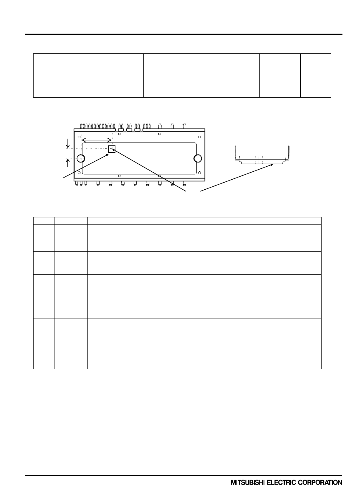
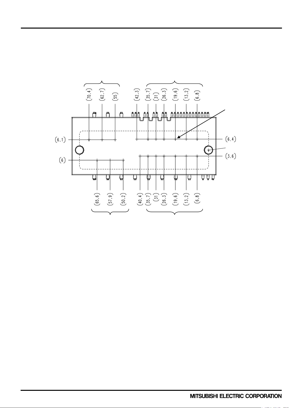
Table 2-1-6. Mechanical characteristics and specifications of PSS25MC1FT (25A/1200V, CIB type)
Parameter Condition
Mounting torque Mounting screw : M4 (Note 10) Recommended 1.18N·m 0.98 1.18 1.47 N·m
(Note 11)
Min. Typ. Max.
-
-
-
Note 10: Plain washers (ISO 7089~7094) are recommended.
Note 11: Measurement positions of heat radiati on part flatness are as below.
Unit
-
Publication Date: September 2016
13
Page 14
< Dual-In-Line Package Intelligent Power Module >
V
N1
N
C
Shunt resistor
P V U W N-side IGBTs
P-side IGBTs
Drive circuit
SC protection circuit
CIN
DIPIPM
R
External parts
Lower-side control
input
Protection circuit state
Internal IGBT gate
Output current Ic
Sense voltage of
the
Error output Fo
SC trip current level
a2
SET
RESET
SC reference voltage
a1
a3
a6
a7
a4
a8
a5
Delay by RC filtering
SC protection level
Collector current Ic
Input pulse width tw (μs)
2
0
Collector
waveform
DIPIPM+ Series Application note
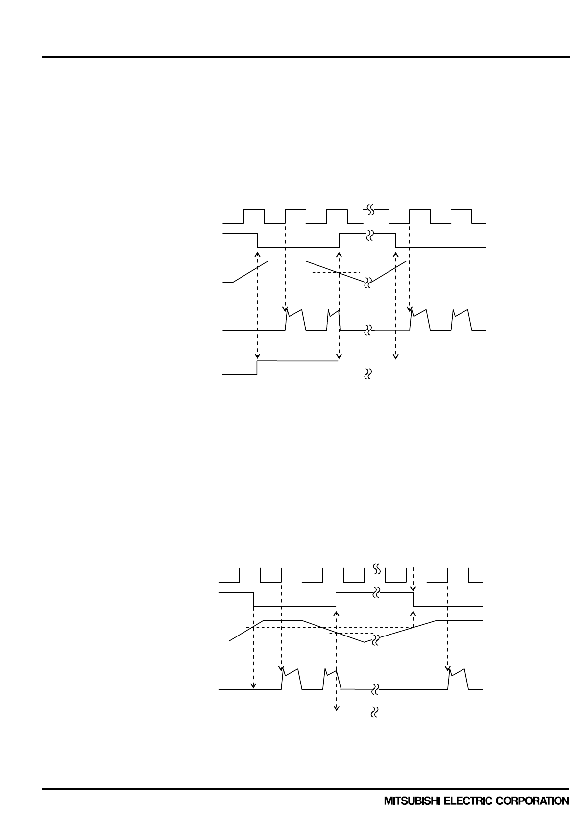
2.2 Protection functions a nd operating sequence DIPIPM+ has two protec t io n f unc tions of s hort c irc uit ( SC ) an d u nder vo lta ge of c ontrol s upp ly (UV). And i t has
also temperature output function of LVIC (VOT). The operating principle and sequence are described as follows.
2.2.1 Short circuit protection (1) Outline
DIPIPM+ uses ex ternal shunt resistor for the current detec tion as shown in F ig.2-2-1. The intern al protection
circuit inside the IC ca ptures the excessive large curr ent by comparing the CIN voltage ge nerated at the shunt
resistor with the ref erenced SC tr ip voltage , and perf orm protec tion autom aticall y. The thres hold voltage tr ip leve l
of the SC protection Vsc(ref) is 0.48V typical.
In case of SC protec tion works, all the gates of N-side thr ee phase IGBTs will be interrupted t ogether with a
fault signal output. To prevent DIPIPM+ erroneous protection due to normal switching noise and/or recovery
current, it is necessar y to set an RC f ilter (tim e constant: 1.5μ ~ 2μs) to the CIN t erminal input (Fi g.2-2-1, 2-2-2).
Also, please make the pattern wiring around the shunt resistor as short as possible.
NC
Fig.2-2-1 SC protection circuit Fig.2-2-2 Filtering time constant setting
Drive circuit
Current
(2) SC protection sequence for only low-side with external shunt resistor and RC filter
a1. Normal operation: IGBT ON and outputs current.
a2. Short circuit current detection (SC trigger)
(It is recommended to set RC time constant 1.5~2.0μs so that IGBT shut down within 2.0μs when SC.)
a3. All N-side IGBT's gates are hard interrupted.
a4. All N-side IGBTs turn OFF.
a5. LVIC starts outputting fault signal (fault signal output time is controlled by external capacitor C
a6. Input = “L”: IGBT OFF
a7. Fo finishes output, but IGBTs don't turn on until inputting next ON signal (LH).
(IGBT of each phase can return to normal state by inputting ON signal to each phase.)
a8. Normal operation: IGBT ON and outputs current.
shunt resistor
Fig.2-2-3 SC protection timing chart
FO
)
Publication Date: September 2016
14
Page 15

< Dual-In-Line Package Intelligent Power Module >
Symbol
Condition
Min
Typ
Max
Unit
V
SC(ref)
Tj=25°C, VD=15V
0.455
0.480
0.505
V
Condition
min.
typ.
max.
Unit
Tj=25°C, VD=15V
34.7
38.4
42.5
A
)1ln(1
)1(
1
cshunt
SC
t
cshuntSC
IR
V
t
IRV
⋅
−⋅−=
−⋅⋅=
−
τ
ε
τ
Item
Min
typ
max
Unit
IC transfer delay time
-
-
1.0
μs
DIPIPM+ Series Application note
(3) Calculation of shunt resistance
The value of current sensing shunt resistance for current sensing is calculated by the following formulation:
= V
R
Shunt
The maximum SC trip level SC(max) should be set less than the IGBT minimum saturation current which is 1.7
times as large as th e rated current. F or example, t he SC(max) of PSS25MC1FT s hould be set to 25x 1.7=42.5A.
The parameters ( V
of DIPIPM+ series is +/-0.025V in the specification of V
Table 2-2-1 Specification for V
Therefore, the rang e of SC trip level can be c alculated b y the following d escriptions w ith +/-5% disp ersion of
shunt resistor :
R
Shunt(min)=VSC(ref) max
where SC(max) is 1.7 times of rated current, and so 0.95 is due to -5% dispersion of shunt resistor that
R
Shunt(typ)
Therefore, SC(typ) = V
R
Shunt(max)
Therefore, SC(min)= V
In this case, SC trip level is 42.5A,
R
Shunt(min)
When the both of SC tr ip level and s hunt resis tor will be m aximum, t ypical and m inimum, these will be des cribed
as follows;
SC(max)= 42.5 A (setting), SC (typ) = 0.480 / 12.5 = 38.4 A, SC(min) = 0.455 / 13.1 = 34.7 A
From the above, the SC trip level range is described as Table 2-2-2.
Table 2-2-2 Operative SC Range
/SC where V
SC(ref)
SC(ref)
, R
) dispersion s hould be c onsid ered w hen d esignin g the SC tr ip le vel. The dispersion
Shunt
SC(ref)
SC(ref)
/SC(max)
= R
= R
Shunt(min)
Shunt(typ)
/ 0.95
SC(ref) typ
/ R
Shunt(typ)
x 1.05* *1.05 is due to +5% dispersion of shunt resistor
SC(ref) min
/ R
Shunt(max)
= 0.505V / 42.5A = 11.9 mΩ, R
is the SC trip voltage.
as shown in Table 2-2-1.
SC(ref)
.
= 11.9mΩ / 0.95 = 12.5 mΩ, R
Shunt(typ)
Shunt(max)
= 12.5 x 1.05 = 13.1mΩ
There is the possibility that the actual SC protection level becomes less than the calculated value. This is
considered due to the resonant signals caused mainly by parasitic inductance and parasitic capacitance. It is
recommended to make a confirmation of the resistance by prototype experiment.
(4) RC filter time constant
It is necessar y to s e t a n R C f ilter i n the S C s e ns ing ci r c uit in or der to prevent m al f unc tion of SC protection due
to noise interferenc e. The RC time cons tant is determined dep ending on the appl ying time of noise interf erence
and the SCSOA of the DIPIPM.
When the voltage dro p on the external shunt resisto r exceeds the SC trip level, The tim e (t1) that the CIN
terminal voltage rises to the referenced SC trip level can be calculated by the following expression:
Where Vsc is the CIN terminal input voltage, Ic is the peak current, τ is the RC time constant.
On the other hand, t he typical t ime dela y t2 (from Vs c voltage reaches Vsc(ref ) to IGBT ga te shutdown) of IC
is shown in Table 2-2-3.
Table 2-2-3 Internal time delay of IC
Therefore, the total delay time from an SC level current happened to the IGBT gate shutdown becomes:
Publication Date: September 2016
t
TOTAL
=t1+t2
15
Page 16

< Dual-In-Line Package Intelligent Power Module >
Control supply voltage
(VD, VDB)
In this voltage range, built-in control IC may not work properly. Normal
xternal noise may cause DIPIPM
starts-up.
UV function becomes active and output Fo (N-side only).
Even if control signals are applied, IGBT does not work.
UVDt (N)-13.5V
UV
DBt
(P)-13.0V
IGBT can work. However, conducting loss and switching loss will increase, and
result extra temperature rise at this state,.
13.5-16.5V (N)
13.0-18.5V (P)
16.5-20.0V (N)
18.5-20.0V (P)
IGBT works. However, switching speed becomes fast and saturation current
becomes large at this state, increasing SC broken risk.
20.0V- (P, N)
The control circuit might be destroyed.
DIPIPM+ Series Application note
2.2.2 Control Supply UV Protect ion The UV prot ection is designed to prevent u nexpected operating behavior as described in Table 2-2-4. Both P-side, N-side of inverter part and Brak e part have UV protecting functi on. However fault s ignal(Fo) output only corresponds to N-side UV protection. Fo output continuously during UV state. In addition, there is a no ise filter (typ. 10μs) integr at ed i n t he UV protection circ uit t o pr e vent insta ntan eous UV erroneous trip. Therefore, the control signals are still transferred in the initial 10μs after UV happened.
Table 2-2-4 DIPIPM operating behavior versus control supply voltage
Operating behavior
operating of each protection function (UV, Fo output etc.) is not also assured.
0-4.0V (P, N)
Normally IGBT does not work. But e
malfunction (turns ON) , so DC-link voltage need t o s ta r t up af ter contr ol supply
4.0-UVDt (N), UV
(note) Ripple Voltage Limitation of Control Supply
If high frequency noise superimpos ed to the control supp ly line, IC m alfunction might happ en and cause
DIPIPM erroneous operation. To avoid such problem happens, line ripple voltage should meet the
following specifications:
dV/dt
(P)
DBt
Recommended conditions.
≤ +/-1V/μs, Vripple ≤ 2Vp-p
Publication Date: September 2016
16
Page 17
< Dual-In-Line Package Intelligent Power Module >
UVDr
RESET
SET
RESET
UVDt
a1
a2
a3
a4
a6
a7
a5
Control input
Protection circuit state
Control supply voltage VD
Output current Ic
Error output Fo
Control input
Protection circuit state
Control supply voltage VDB
Output current Ic
Error output Fo
UV
RESET
SET
RESET
UV
Keep High-level (no fault output)
a1
a2
a3
a4
a5
a6
DIPIPM+ Series Application note
(1) N-side UV Protection Sequence
a1. Control supp ly voltage V
ON signal (LH).
(IGBT of each phase can return to normal state by inputting ON signal to each phase.)
a2. Normal operation: IGBT ON and carrying current.
level dips to under v olta ge tr ip le vel . (UVDt).
a3. V
D
a4. All N-side IGBTs turn OFF in spite of contr ol input c ondit io n.
a5. Fo outputs for the period set by the capacitance C
level reaches UVDr.
a6. V
D
a7. Normal operation: IGBT ON and outputs current.
Fig.2-2-4 Timing Chart of N-side UV protection
(2) P-side UV Protection Sequence
a1. Control supply voltage V
IGBT turns on by next ON signal (LH).
a2. Normal operation: IGBT ON and outputs current.
a3. V
level drops to under voltage trip level (UV
DB
a4. IGBT of the corresponding phase only turns OFF in spite of control input signal level,
but there is no F
a5. V
level reaches UV
DB
signal output.
O
a6. Normal operation: IGBT ON and outputs current.
Fig.2-2-5 Timing Chart of P-side UV protection
exceeds under voltage reset level (UVDr), but IGBT turns ON by next
D
but output is extended during VD keeps below UVDr.
FO,
rises. After the voltage r eac hes under voltage reset level UV
DB
).
DBt
.
DBr
DBr
DBt
DBr
,
Publication Date: September 2016
17
Page 18

< Dual-In-Line Package Intelligent Power Module >
Control input
Protection circuit state
Control supply voltage VD
Output current Ic
Error output Fo
UV
RESET
SET
RESET
UVDt
Keep High-level (no fault output)
a1
a2
a3
a4
a5
a6
DIPIPM+ Series Application note
(3) Brake UV Protection Sequence ( with Brake product only : PSSxxMC1Fx)
a1. Control supply voltage V
IGBT turns on by next ON signal (LH).
a2. Normal operation: IGBT ON and collector current.
level drops to under vo ltag e trip level (UVDt).
a3. V
D
a4. IGBT of the corresponding phase only turns OFF in spite of control input signal level,
but there is no F
level reaches UVDr.
a5. V
D
signal output.
O
a6. Normal operation: IGBT ON and outputs current.
Fig.2-2-6 Timing Chart of brake circuit UV protect ion
rises. After the voltage reaches under voltage reset level UVDr,
D
Dr
Publication Date: September 2016
18
Page 19

< Dual-In-Line Package Intelligent Power Module >
min.
Source
1.7mA
Sink
0.1mA
Ref
VOT
Temperature
signal
VNC
Inside LVIC
of
5V
MCU
Ref
VOT
Temperature
signal
VNC
Inside LVIC
of
5.1kΩ
LVIC
Power chip area
Heatsink
IGBT
LVIC
FWDi
Temperature of
DIPIPM+ Series Application note
2.2.3 Temperature output function V
(1) Usage of this function
This function measures the temperature of control LVIC by built in temperature sensor on LVIC.
The heat generated at IGBT and FWDi transfers to LVIC through molding resi n of pac k age and outer heat sink.
So LVIC temperature cannot respo nd to rapid tem perature r ise of those p ower chips effectivel y. (e.g. motor lock,
short circuit). It is recom mended to use this f unction for protectin g from slow exces sive temperature rise by such
cooling system down and continuance of overload operation. (Replacement from the thermistor which was
mounted on outer heat sink currently)
(note)
In this function, DIPIPM cannot shutdown IGBT and output fau lt signal by itself when temperature rises
excessively. W hen temperature exceeds the defined protection level, controller (MCU) should s top the
DIPIPM.
(Detecting point)
Fig.2-2-7 Temperature detecting point Fig.2-2-8 Thermal conducting from power chips
(2) VOT characteristics
VOT output circuit, which is des cribed in Fig.2-2-9, is the o utput of OP am plifier circuit. The c urrent capabilit y
of VOT output is described as Table 2-2-5. The characteristics of VOT output vs. LVIC temperature is linear
characteristics described in Fig.2-2-11. There are some cautions for using this function as follows.
Table 2-2-5 Output capability
(Tc=-20°C ~100°C)
OT
LVIC is affected
from heatsink.
DIPIPM
Publication Date: September 2016
Source: Current flow from V
Sink : Current flow from outside to V
to outside.
OT
.
OT
Fig.2-2-9 VOT output circuit
(note) In the case of detecting lower temperature than room temperature
It is recommended to insert 5.1kΩ pull down resistor for getting linear output characteristics at lower
temperature than room temperature . W hen the pull do wn resis tor is inser ted bet ween V
GND), the extra current calculated by V
current continuously. In the case of only using V
output voltage / pull down resistance flows as LVIC circuit
OT
for detecting higher temperature than room
OT
and VNC(control
OT
temperature, it isn't necessary to insert the pull down resistor.
Fig.2-2-10 V
output circuit in the case of detecting low temperature
OT
DIPIPM
MCU
19
Page 20

< Dual-In-Line Package Intelligent Power Module >
0
0.2
0.4
0.6
0.8
1
1.2
1.4
1.6
1.8
2
2.2
2.4
2.6
2.8
3
3.2
3.4
3.6
3.8
4
-30 -20 -10 0 10 20 30 40 50 60 70 80 90 100 110 120 130
VOT out put [V]
LVIC temperature [degC]
3.14
3.02
2.89
Max. Min. Typ.
Output range without 5.1kΩ pull down resistor
Output range with 5.1kΩ pull down resistor
DIPIPM+ Series Application note
←
(Output might saturated under this level)
←
(Output might saturated under this level)
Fig.2-2-11 V
output vs. LVIC temperature
OT
Publication Date: September 2016
20
Page 21

< Dual-In-Line Package Intelligent Power Module >
with brake type
without brake type
DIPIPM+ Series Application note
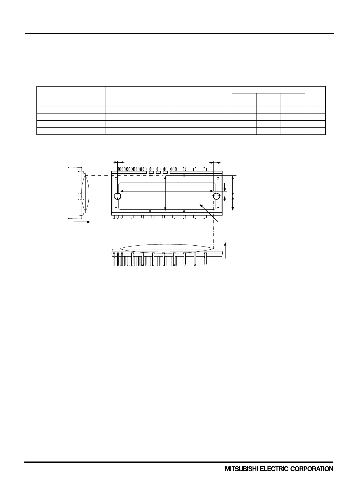
2.3 Package outline of DIPIPM+
2.3.1 Package outline
Fig. 2-3-1 Package outline drawing (Dimension in mm)
Publication Date: September 2016
21
Page 22

< Dual-In-Line Package Intelligent Power Module >
Country of origin
DIPIPM+ Series Application note
2.3.2 Marking
The laser marking specifications of DIPIPM+ are described in Fig.2-3-2. Company name, Country of origin,
Type name, Lot number, and 2D code are marked on the surface of module.
Fig.2-3-2 Laser marking view PSSxxxC1Fx (Dimension in mm)
The Lot number indicates production year, month, running number and country of origin.
The detailed is described as below.
(Example)
6 9 AA1
Running number
Product month (however O: October, N: November, D: Decem ber)
Last figure of Product year (e.g. This case describes the year 2016.)
Publication Date: September 2016
22
Page 23

< Dual-In-Line Package Intelligent Power Module >
PSSxxMC1Fx
PSSxxNC1Fx
With Brake
Without Brake
1
P1
Output terminal for converter (+)
2
N1
Output terminal for converter (-)
3
N(B)
(NC)
IGBT emitter terminal for brake
4
V
NC
*1)
Control supply GND terminal (Brake part)
5
AlN
(NC)
Brake part control input terminal
6
V
P1
*2)
Control supply positive terminal (+)
7
V
UFB
U-phase P-side drive supply positive terminal
8
V
UFS
U-phase P-side drive supply GND terminal
9
V
VFB
V-phase P-side drive supply positive terminal
10
V
VFS
V-phase P-side drive supply GND terminal
11
V
WFB
W-phase P-side drive supply positive terminal
12
V
WFS
W-phase P-side drive supply GND terminal
13
UP
U-phase P-side control input terminal
14
VP
V-phase P-side control input terminal
15
WP
W-phase P-side control input terminal
16
V
P1
*2)
Control supply positive terminal (+)
17
UN
U-phase N-side control input terminal
18
VN
V-phase N-side control input terminal
19
WN
W-phase N-side control input terminal
20
Fo
Fault signal output terminal
21
VOT
Temperature output terminal
22
CIN
SC current trip voltage detecting terminal
23
CFo
Fault pulse output width setting terminal
24
VN1
N-side control supply positive terminal (+)
25
V
NC
*1)
GND terminal for brake control supply
26
NW
WN-phase IGBT emitter terminal
27
NV
VN-phase IGBT emitter terminal
28
NU
UN-phase IGBT emitter terminal
29
W
W-phase output terminal
30
V
V-phase output terminal
31
U
U-phase output terminal
32
P
Inverter DC-link positive terminal
33 B (NC)
Brake terminal
34
T
AC input terminal
35
S
AC input terminal
36
R
AC input terminal
DIPIPM+ Series Application note
2.3.3 Terminal Description
Table 2-3-1 Terminal Description
(note)
1) Two V
connect either terminal to GND and make the other terminal leave no connection.
2) Two V
other terminal leave no connection.
terminals (GND ter minal for control supply) ar e connected mutually inside of DIPIPM+, pleas e
NC
term inals are connected mutually inside, please c onnect either ter minal to suppl y and m ake the
P1
Description
NC: No connection
Publication Date: September 2016
23
Page 24

< Dual-In-Line Package Intelligent Power Module >
Item
Symbol
Description
P-side drive
V
- V
Drive supply terminals for P-side IGBTs.
terminals is helpful to prevent control IC from surge destruction.
P-side control
V
Control supply terminals for the built-in HVIC and LVIC.
control supply terminals to prevent surge destruction.
N-side control
VNC
Control ground terminal for the built-in HVIC and LVIC.
through this terminal in order to avoid noise influences.
Control input
UP,VP,WP
Control signal input terminals. This is Voltage input type.
resistor.
Short-circuit trip
terminal
CIN
For short circuit protection, input the potential of external shuint res istor to
The time constant of RC filter is recommended to be up to 2μs.
Fault signal
FO
Fault signal output terminal for N-side abnormal state(SC or UV).
increasing I
FO.
)
Fault pulse output
CFO
The terminal is for setting the fault pulse output width.
2.4ms. Because of CFO = t
FO
x 9.1 x 10⁻⁶ (F)
Temperature
VOT
LVIC temperature is ouput by analog signal. It is ouput of OP amplifer
necessary under room temperature.
Inverter DC-link
P
DC-link positive power supply terminal.
characteristics for snubber.
DIPIPM+ Series Application note
Table 2-3-2 Detailed description of input and output terminals
supply
positive terminal
P-side drive
supply
GND terminal
supply terminal
N-side control
supply terminal
GND terminal
terminal
UFB
V
- V
VFB
- V
V
WFB
P1
V
N1
UN,VN,W
AlN
UFS
VFS
WFS
•
• By mounting bootstrap ca pacitor, individ ual isolated p ower supplies are not
needed for the P-s ide IGBT drive. Each bootstrap capacitor is charged b y
the N-side V
• Abnormal operation might happen if the V
supply when potential of output terminal is almost GND level.
D
supply is not aptly stabilized or
D
has insufficient current capability due to ripple or surge. In order to prevent
malfunction, a bypass capacitor with favorable frequency and temperature
characteristics should be mounted very closely to each pair of these
terminals.
• Inserting a Zener diode (24V/1W) between each pair of control supply
•
• V
, and VN1 should be connected externall y on PCB. In order to prevent
P1
malfunction caused by noise and ripple in the supply voltage, a bypass
capacitor with go od f r eque ncy characteristics shou ld be m ounted ver y close
to these terminals.
• Please design the supply carefully so that the voltage ripple caused by
operation keep within the specification. (dV/dt ≤ +/-1V/μs, Vripple≤2Vp-p)
• It is recommended to insert a Z ener diode (24V/1W) between eac h pair of
•
• Please make sure that line current of the power circuit does not flow
•
N
• These terminals are internally connecte d to Schmitt trigger circuit and pulled
down by min 3.3kΩ resistor internally
• The wiring of each input should be as short as possible to protect the
DIPIPM from noise interference.
• Please use RC coupling in case of signal oscillation. Pay attention to
threshold voltage of input terminal, because input circuit has pull down
•
voltage detecting
output terminal
CIN terminal through RC filter (for the noise immunity).
•
•
• This output is open drain t ype. I t is r ecom mended to pull up F
the 5V supply by 10kΩ when Fo signal is input to MCU directly (Check
whether the V
resistance).
• In the case of directl y driving opto coupler b y Fo output it is needed to set
the pull-up resistance so that I
And pulled up to 15V suppl y is recommended.(V
•
width setting
terminal
output terminal
positive terminal
• An external capacitor should be connected between this terminal and V
When 22nF capacitor is connected, then the Fo pulse width becomes
•
internally.
• It is recommended to con nect 5.1kΩ pulldo wn resistor if output linearl ity is
•
• Internally connected to the collectors of all P-side IGBTs.
• To suppress surge voltage caused by DC-link wiring or PCB pattern
inductance, smoothing capacitor should be inserted very closely to the P
terminal. It is also eff ective to add small film capacitor with good frequenc y
signal lin e to
O
satisies t he thresh old le vel of inpu t of MCU when s electing
FO
becomes under 5mA(maximum rating).
FO
increases in propo tion to
FO
NC
.
Publication Date: September 2016
24
Page 25

< Dual-In-Line Package Intelligent Power Module >
Item
Symbol
Description
Inverter DC-link
NU, NV, NW
Emitter terminal of each N-side IGBT
terminals together at the point as close from the package as possible.
Inverter power
U, V, W
Inverter output terminals for connection to inverter load (e.g. AC motor).
corresponding IGBT half bridge arm.
AC power supply
input terminal
R, S, T
AC power supply input terminal
Converter positive
output terminal
P1
Converter positive output terminal
Converter GND
terminal
N1
Converter GND terminal
DIPIPM+ Series Application note
(Continue)
•
negative terminal
output terminal
(note)
Use oscilloscope to check voltage waveform of each po wer supply terminals and P and N term inals, the
time division of OSC should be set to about 1μs/div. Please ensure the voltage (including surge) not
exceed the specified limitation.
If there is a surge more than threshold of ratings or superimposed noise, it is necessary to take some
counter noise m easurements; revising pattern, rep lacing capacitor, apply zener diode, enh ancing filtering
and so on.
• Usually, these terminals are connected to the power GND through individual
shunt resistor.
• If common emitter circuit (one shunt control) is applied, connect these
•
• Each terminal is internally connected to the intermidiate point of the
•
•
•
Publication Date: September 2016
25
Page 26

< Dual-In-Line Package Intelligent Power Module >
Clearance(mm)
Creepage(mm)
Between power terminals
5.8
Between power terminals
6.0
Between control terminals
2.5
Between control terminals
6.4
Between terminals and heat sink
2.5
Between terminals and heat sink
4.3
(1)
(2)
DIPIPM+ Series Application note
2.4 Mounting Method This section are describe d the electric spacing and mounting precautions of DIPIPM+.
2.4.1 Electric Spacing of DIPIPM + The electric spacing specification of DIPIPM+ is shown in Table 2-4-1.
Table 2-4-1 Minimum insulation distance(minimum value)
2.4.2 Mounting Method and Precautions When installing the modul e to the heat sink , excessive or uneven fasten ing force m ight apply stress to inside chips. Then it will lead to a broken or degradation of the c hips or insu lat ion s truc tu r e. T he r ec ommended fastening procedure is shown in Fig.2-4-1. When f astening, it is necessary to use the torque wrenc h and fasten up to th e specified torque. And pay attention not to have any foreign par ticle on the contact sur face between the modu le and the heat sink. Even if the f ixing of heatsi nk was d one b y proper proc edure a nd condition, there is a pos s ibilit y of damaging the pac kage bec ause of tightening by unexpected excessive torque or tuck ing partic le. For ens uring safety it is recom mended to conduct the confirm ation test (e.g. insulation inspection) on the f inal product after fixing the DIPIPM with the heatsink.
Fig.2-4-1 Recommended screw fastening order
Temporary fastening
(1)→(2)
Permanent fastening
(1)→(2)
Note: Generally, the temporary fastening torque is set to
20-30% of the maximum torque rating.
Not care the order of fastening (1) or (2), but need to
fasten alternately.
Publication Date: September 2016
26
Page 27

< Dual-In-Line Package Intelligent Power Module >
Item
Condition
Min.
Typ.
Max.
Unit
Mounting torque
Screw : M4
0.98 -
1.47
N・m
Flatness of outer heat sink
Refer Fig.2-4-2
-50 -
+100
μm
+
+
Measurement position
Outer heatsink
Measurement position
Aluminum Heatsink
DIPIPM+ Series Application note
Table 2-4-2 Mounting torque and heat sink flatness specifications
(note): Recommend to use plain washer (ISO7089-7094) in fastening the screws.
Fig.2-4-2 Measurement positions of heat radiation part flatness
In order to get effective heat d issipation, it is necessary to enlarge t he contact area as much as pos sible to
minimize the contact t hermal resistance. Regarding the he at sink flatness (war p/concavity and con vexity) on the
module installation surface, the surface finishing-treatment should be within Rz12.
Evenly apply thermally-conductive grease with 100μ-200μm thickness over the contact surface between a
module and a heat sink, whic h is also useful for preventing corrosion. Furtherm ore, the grease should be with
stable quality and long-term endurance within wide operating temperature range. The contacting thermal
resistance between DIPIPM case and heat sink Rth(c-f) is determined by the thickness and the thermal
conductivity of the applied grease. For referenc e, Rth(c-f) is about 0.25K/W (per chip, grease thickness: 20μm,
thermal conductivity: 1.0W/m·k). W hen applying grease and fixing heat sink, pay attention not to take air into
grease. It might lead to make contact thermal resistance worse or loosen fixing in operation.
-
Publication Date: September 2016
27
Page 28

< Dual-In-Line Package Intelligent Power Module >
Item
Condition
DIPIPM+ Series Application note
2.4.3 Soldering Conditions The recommended soldering condition is mentioned as below. (Note: The reflow soldering cannot be recommended for DIPIPM.)
(1) Flow (wave) Soldering
DIPIPM is tested on the condition described in Table 2-4-3 about the soldering thermostability, so the
recommended conditions for flow (wave) soldering are soldering temperature is up to 265°C and the
immersion time is within 11s.
The actual cond ition might need som e adjustment based on its flow condition of solder, the speed of the
conveyer, the la nd pat ter n and the t hr oug h ho le s h ape on th e PC B, etc. It is necessary to confirm whether it is
appropriate or not for your real PCB finally..
Table 2-4-3 Reliability test specification
Soldering thermostability 260±5°C, 10±1s
(2) Hand soldering
Since the temperature impressed upon the DIPIPM may changes based on the soldering iron types
(wattages, shape of soldering tip, etc.) and the land pattern on PCB, the unambiguous hand soldering
condition cannot be decided.
As a general requirem ent of the temperatur e profile for hand s oldering, the temper ature of the root of the
DIPIPM terminal should be kept less than 150°C for considering glass transition temperature (Tg) of the
package molding resin and the thermal withstand capability of internal chips. Therefore, it is necessary to
check the DIPIPM terminal root temperature, solderability and so on in your real PCB, when configure the
soldering temperature profile. (It is recommended to set the soldering time as short as possible.)
Publication Date: September 2016
28
Page 29

< Dual-In-Line Package Intelligent Power Module >
C1: Electrolytic type with good temperature and frequency characteristics
Z : Surge absorber
C : AC filter(ceramic capacitor 2.2n
Drive circuit
UV lockout
circuit
Level shift
Input signal
conditioning
Drive circuit
Level shift
Input signal
conditioning
Drive circuit
Level shift
Input signal
conditioning
Drive circuit
UV lockout
circuit
Fo Logic
Input signal
conditioning
P-side input
Fo
Fo output
V
N1
N CIN
V
NC
V
D
(15V line)
C1
C2
N-side input
Inrush
P V U W
M
AC output
N-side IGBTs
P-side IGBTs
AC line input
DIPIPM+
(CIB type)
Protection
D1
C3
C1
C2
D1
UV lockout
circuit
UV lockout
circuit
CFo
Drive circuit
UV lockout
circuit
Brake input
Temp. output
VOT
B
Input signal
conditioning
Braking
resistor
N(B)
Brake IGBT
Brake Di
Z
C
P
N1
R S T
DIPIPM+ Series Application note
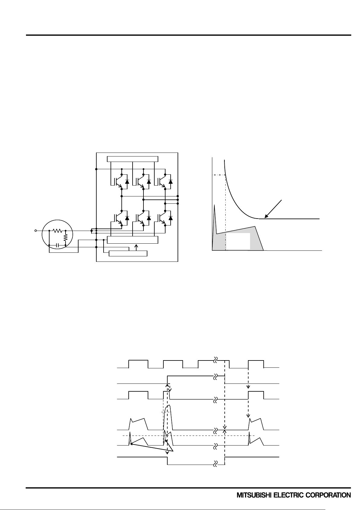
CHAPTER 3 : SYSTEM APPLICATION GUIDANCE
3.1 Application guidance This chapter states the DIPIPM+ application method and interface circuit design hints.
3.1.1 System connection
(note) The capacitance also depends on the PWM
control strategy of the application system
C2: 0.01μ-2μF ceramic capacitor with good temperature,
frequency and DC bias characteristics
C3: 0.1μ-0.22μF Film capacitor (for snubber)
D1: Zener diode 24V/1W for surge absorber
(Common-mode noise filter)
-6.5nF)
limiting circuit
NC
Fig.3-1-1 System block diagram (Example)
circuit (SC)
Publication Date: September 2016
29
Page 30

< Dual-In-Line Package Intelligent Power Module >
Long GND wiring might generate noise to input signal
and cause IGBT malfunction
M
MCU
C2
15V
VD
C4
R1
Shunt resistor
N1
C
5V
+
C1
D
D1
C3
+
R2
5.1kΩ
C2 + C1 D1 C2
C5
R3
C5
R3
Brake
Resistor
Prevention circuit
for
P (32)
U (31)
V (30)
W (29)
NW (26)
LVIC
NV (27)
NU (28)
HVIC
S (35)
T (34)
B (33)
LVIC
Power GND patterning
Control GND patterning
C5
R3
C5
R3
C5
R3
C5
R3
C5
R3
+
+
A
B
UN (17)
VN (18)
WN (19)
Fo (20)
V
(9)
VP (14)
V
(11)
WP (15)
UP (13)
V
(25)
V
(16)
V
(7)
V
(21)
P1(1)
N1 (2)
N(B) (3)
AIN (5)
V
NC
(4)
V
(6)
V
(8)
V
VFS
(10)
V
(12)
R (36)
V
(24)
CIN (22)
CFo (23)
X
Y
X
Y
Long wiring might cause short
AC input
Long wiring might cause SC level fluctuation
DIPIPM+ Series Application note
3.1.2 Interface Circuit (Direct Coupling Interface example for using one shunt resistor) Fig.3-1-2 shows a t ypical a pplicati on circui t of inter fac e schem atic , in which co ntrol sig nals are transf erred di rect ly input from a controller (e.g. MCU).
inrush current
P1
UFB
UFS
VFB
WFB
WFS
P1
OT
N1
NC
Fig.3-1-2 Interface circuit example in the case of using with one shunt resistor
and malfunction
circuit failure
Publication Date: September 2016
30
Page 31

< Dual-In-Line Package Intelligent Power Module >
DIPIPM+ Series Application note
Note for the previous application circuit:
(1) If control GND is connected with power GND by common broad pattern, it may cause malfunction by power GND fluctuation. It
is recommended to connect control GND and power GND at only a point N1 (near the terminal of shunt resistor).
(2) It is recommended to insert a Zener diode D1(24V/1W) between each pair of control supply terminals to prevent surge
destruction.
(3) To prevent surge destruction, the wiring between the smoothing capacitor and the P, N1 terminals should be as short as
possible. Generally a 0.1-0.22μF snubber capacitor C3 between the P-N1 terminals is recommended.
(4) R1, C4 of RC filter for preventing protection circuit malfunction is recommended to select tight tolerance, temp-compensated
type. The time constant R1C4 should be set so that SC current is shut down within 2μs. (1.5μs~2μs is recommended
generally.) SC interrupting time might vary with the wiring pattern, so the enough evaluation on the real system is necessary.
(5) To prevent malfunction, the wiring of A, B, C should be as short as possible.
(6) The point D at which the wiring to CIN filter is divided should be near the terminal of shunt resistor. NU, NV, NW terminals
should be connected each other at near those three terminals when it is used by one shunt operation. Low inductance SMD
type with tight tolerance, tem p-compensated type is recommended for shunt resistor.
(7) All capacitors should be mounted as close to the terminals as possible. (C1: good temperature, frequency characteristic
electrolytic type and C2:0.01μ-2μF, good temperature, frequency and DC bias characteristic ceramic type are recommended.)
(8) Input logic is High-active. There is a 3.3kΩ(min.) pull-down resistor in the input circuit of IC. To prevent malfunction, the input
wiring should be as short as possible. When using RC coupling, make the input signal level meet the turn-on and turn-off
threshold voltage.
(9) Fo output is open drain type. Fo output will be max 0.95V(@I
supply (e.g. 5V,15V) by a resistor that makes I
up to 1mA. (In the case of pulled up to 5V, 10kΩ is recommended.) About
FO
driving opto coupler by Fo output, please refer the application note of this series.
(10) Fo pulse width can be set by the capacitor connected to CFO terminal. C
(11) If high frequency noise superimposed to the control supply line, IC malfunction might happen and cause DIPIPM erroneous
operation. To avoid such problem, line ripple voltage should meet dV/dt ≤+/-1V/μs, Vripple ≤ 2Vp-p.
(12) For DIPIPM, it isn't recommended to drive same load by parallel connection with other phase IGBT or other DIPIPM.
(13) No.4 and No.25 V
No.16 V
terminals are connected mutually inside, please connect either No.4 or No.25 terminal to GND and also connect
P1
terminals (GND terminal for control supply) are connected mutually inside of DIPIPM+ and also No.6 and
NC
either No.6 or No.16 terminal to supply and make the unused terminal leave no connection.
=1mA,25°C), so it should be pulled up to MCU or control power
FO
(F) = 9.1 x 10⁻⁶ x tFO (Required Fo pulse width).
FO
Publication Date: September 2016
31
Page 32

< Dual-In-Line Package Intelligent Power Module >
Long GND wiring might
generate noise to input signal
and cause IGBT malfunction
M
C2
15V
VD
C4
R1
Shunt resistor
N1
C
+
C1
D
D1
C3
+
5.1kΩ
C2
+
C1 D1 C2
C5
R3
C5
R3
Brake
Resistor
Prevention circuit
for
P (32)
U (31)
V (30)
W (29)
NW (26)
LVIC
NV (27)
NU (28)
HVIC
S (35)
T (34)
B (33)
LVIC
Power GND patterning
Control GND patterning
C5
R3
C5
R3
C5
R3
C5
R3
C5
R3
+
+
A
B
UN (17)
VN (18)
WN (19)
Fo (20)
V
(9)
VP (14)
V
(11)
WP (15)
UP (13)
V
(25)
V
(16)
V
(7)
V
(21)
P1(1)
N1 (2)
N(B) (3)
AIN (5)
V
NC
(4)
V
(6)
V
(8)
V
(10)
V
(12)
R (36)
V
(24)
CIN (22)
CFo (23)
X
Y X Y
Long wiring might cause short
circuit failure
AC input
Long wiring might cause SC level fluctuation
and malfunction
OT trip
level
Comparator
-
MCU
5V
DIPIPM+ Series Application note
3.1.3 Interface circuit (example of opto-coupler isolated interface)
(note)
(1) High speed (high CMR) opto-coupler is recommended.
(2) Set the current limiting resistance to make Fo sink current IFO=5mA or less when the opto-coupler is driven by Fo output
directly. To assure I
(3) To prevent malfunction, it is strongly recommended to insert RC filter (e.g. R3=100Ω and C5=1000pF) and confirm the input
signal level to meet turn-on and turn-off threshold voltage.
(4) About comparator circuit at V
output chattering.
Publication Date: September 2016
+
inrush current
P1
UFB
UFS
VFB
VFS
WFB
WFS
P1
OT
N1
NC
Fig.3-1-3 Interface circuit example with opto-coupler
=5mA, it will be needed to pull up to 15V supply since Fo output may be max 4.75V (@IFO=5mA, 25℃).
FO
output, it is recommended to design the input circuit with hysteresis because of preventing
OT
32
Page 33

< Dual-In-Line Package Intelligent Power Module >
Item
Symbol
Condition
Min.
Typ.
Max.
Unit
P
V
U W N-side IG B T
P-side IG BT
Drive circuit
DIPIPM
VNC
NW
Drive circuit
CIN
NV
NU
-
Vref
+
Vref
Vref
Comparators
(Open collector output type)
External protection circuit
Protection circuit
Shunt
resistors
Rf
Cf
5V
B A C
OR output
D
N1
- + -
+
U
, WP
DIPIPM
UN,VN,W
AIN
3.3kΩ(min)
3.3kΩ(min)
Gate drive
circuit
Gate drive
circuit
Level shift
circuit
DIPIPM+ Series Application note
3.1.4 External SC protection circuit wit h using three shunt resistors When using three shunt resistor, protection circuit is described as following Fig.3-1-4.
Fig.3-1-4 Interface circuit example
(note)
(1) It is necessary to set the time constant RfCf of external comparator input so that IGBT stop within 2μs when sho rt c ircuit
occurs.
(2) SC interrupting time might vary with the wiring pattern, comparator speed and so on.
(3) The threshold voltage Vref should be set up the same rating of short circuit trip level (Vsc(ref) typ. 0.48V).
(4) Select the external shunt resistance so that SC trip-level is less than specified value.
(5) To avoid malfunction, the wiring A, B and C should be designed as short as possible.
(6) The point D at which patterns are branched to each comparator should be closer to the terminal of shunt resistor.
(7) OR output high level should be more than 0.505V (=maximum Vsc(ref)).
(8) GND of Comparator, GND of Vref circuit and Cf should be connected to control GND wiring. (not to power GND)
3.1.5 Circuits of Signal Input Terminals and Fo Terminal (1) Internal Circuit of Control Input Terminals
DIPIPM is high-active input logic. 3.3kΩ(min)
pull-down resistor is b ui lt-in eac h input cir cu its of
P, VP
the DIPIPM as show n in Fig.3-1-5 , so external
pull-down resistor is not needed.
Furthermore, the turn-on and turn-off
threshold voltage of input signa l are as sho wn in
N
Table 3-1-1 .
Fig.3-1-5 Internal structure of control input terminals
Table 3-1-1 Input threshold voltage ratings(Tj=25°C)
Turn-on threshold voltage Vth(on)
Turn-off threshold voltage Vth(off)
(note)
(1) The wiring of each input should be patterned as short as possible. If the pattern is long and the noise is imposed on the
(2) There are limits for the minimum input pulse width in the DIPIPM. The DIPIPM might make no response or delayed
Publication Date: September 2016
U
P,VP,WP-VNC
U
N,VN,WN-VNC
AIN-V
terminals,
terminals,
terminal
NC
- - 3.5
0.8 - -
pattern (e.g. Fig3-1-6), it may be effective to insert RC filter.
response, if the input pulse width (both on and off) is shorter than the specified value. (Table 3-1-2)
33
V
Page 34

< Dual-In-Line Package Intelligent Power Module >
UP,VP,WP,UN,VN,WN,AIN
Fo
VNC(Logic)
DIPIPM
MCU/DSP
10kΩ
5V line
3.3kΩ (min)
Item
Symbol
Condition
Min. value
Unit
0≤VCC≤800V(for 1200V series) or
N line wiring inductance less than 10nH
Up to rated
current
From rated
current
P Side Control Input
Internal IGBT Gate
Output Current Ic
t1
t2
Real line : off pulse width>PWIN(off ); turn on time t1
Broken line
DIPIPM+ Series Application note
Fig.3-1-6 Control input connection
(note)
(1) The RC coupling (parts shown as broken line) at each input depends on user’s PWM control strategy and the wiring
impedance of the printed circuit board.
(2) The DIPIPM signal input section integrates a 3.3kΩ(min) pull-down resistor. Therefore, when using an external
filtering resistor, please be careful to the signal voltage drop at input terminal.
Table 3-1-2 Allowable minimum input pulse width
PWIN(on) Up to 1.7 times of rated current 1.5
Allowable
minimum input
pulse width
PWIN(off)
0≤VCC≤350V(for 600V series),
13.5≤V
≤16.5V, 13.0≤VDB≤18.5V,
D
-20°C ≤Tc≤100°C,
current to 1.7
times of rated
3
μs
3.5
(note)
(1) Input signal with ON pulse width less than PWIN(on) might make no response.
(2) IPM might make no response or delayed response for the input OFF signal with pulse width less than PWIN(off).
(Delay occurs for p-side only .) Please refer the following Fig.3-1-7 of delayed response.
: off pulse width<PWIN(off); turn on time t2
(t1:Normal switching time)
Fig.3-1-7 Delayed response of output operation with inputting less than PWIN(OFF) for P-side
Publication Date: September 2016
34
Page 35

< Dual-In-Line Package Intelligent Power Module >
Item
Symbol
Condition
Min.
Typ.
Max.
Unit
V
FOH
VSC=0V, Fo=10kΩ 5V Pulled-up
4.9 - - V V
FOL
VSC=1V, IFO=1mA
-
0.95
V
0.0
0.5
1.0
1.5
2.0
2.5
3.0
0 1 2 3 4 5
V
FO
(V)
IFO(mA)
DIPIPM
P + -
Wiring Inductance
Shunt resistor
NU
DIPIPM+ Series Application note
(2) Internal circuit of Fo terminal
Fo terminal is an open dra in type. W hen Fo out put is input into MCU( controller) directl y, it is necessar y to
note the dependenc y of V
signal level fits to the input threshold voltage of MCU. In the case of pulling up to 5V supply, it is
recommended to pull up by 10kΩ resistor.
When the opto-coup ler is d r iven b y F o ou tput d irec tly, the maximum Fo sink curr ent b ec omes 5mA or less.
To assure I
=5mA, it will be needed to pu ll up to 1 5V suppl y since Fo output m ay be m ax 4.75V (@IFO=5mA,
FO
25°C).
If max 5mA coupler driving current is not enough, it is necessary to apply buffer circuit for increasing
driving current.
Table 3-1-3 shows the typical V-I characteristics of Fo terminal.
on IFO (VFO=max0.95V @IFO=1mA, 25°C) and set pull up resistance so that Fo
FO
Fault output voltage
-
Fig.3-1-8 Fo terminal typical V-I characteristics (V
=15V, Tj=25°C)
D
3.1.6 Snubber circuit In order to prevent DIPIPM from destruction b y extra surge, the wiri ng length b etween th e s moothing capacitor and P terminal (D IPIPM) – N1 points (shunt resistor terminal) should be designed as short as possible. Also, a
0.1μ~0.22μF snubber capacitor with high withstanding voltage should be mounte d in the DC-link and clos e to P
and N1.
In order to suppress the surge voltage maximally, the wiring at part-A (including shunt resistor parasitic
inductance) should be designed as small as possible as shown in Fig.3-1-9.
Fig.3-1-9 Recommended snubber circuit location
NV
NW
Publication Date: September 2016
35
Page 36

< Dual-In-Line Package Intelligent Power Module >
Connect GND wiring from VNC terminal to the
shunt resistor terminal as close as possible.
Shunt
It is recommended to make the inductance of each
e.g.
(width=3mm, length=17mm) is about 10nH.
N1
VNC
DIPIPM
NW
Connect GND wiring from VNC terminal to the
shunt resistor terminal as close as possible.
Shunt
resistor
It is recommended to make the inductance of this part
e.g.
(width=3mm, length=17mm) is about 10nH.
N1
VNC
DIPIPM
NW
DIPIPM+ Series Application note
3.1.7 Recommended wiring method around shunt resistor External shunt resistor is nec essary to detect short -circuit acc ident. If applied a lon ger patterning be tween the shunt resistor and D IPIPM, it causes so m uch large s urge that m ight damage built-in I C. To dec rease th e patter n inductance, the wiring between the shunt resistor and DIPIPM should be connected as short as possible and using low inductance resistor such as SMD (Surface Mounted Device) resistor instead of long-lead resistor.
NU
NV
Fig.3-1-10 Wiring instruction (In the case of using with one shunt resistor)
NU
NV
Fig.3-1-11 Wiring instruction (In the case of using with three shunt resistors)
NU, NV, NW should be connected each other at near terminals.
(including the shunt resistor) under 10nH.
Inductance of copper pattern
phase (including the shunt resistor) less than 10nH.
Inductance of copper pattern
resistors
Publication Date: September 2016
36
Page 37

< Dual-In-Line Package Intelligent Power Module >
Drive circuit
Drive circuit
SC protection
W
V
U
C
VNC
CIN
A
P
N1
N
D
R2
Shunt resistor
DIPIPM
P-side
IGBTs
N-side
IGBTs
Current path
External protection circuit
B
C1
DIPIPM+ Series Application note
Influence of pattern wiring around the shunt resistor is shown below.
Fig.3-1-12 External protection circuit
(1) Influence of the part-A wiring
The ground of N-side IGBT gate is VNC. If part-A wiring pattern in Fig.3-1-12 is too long, extra voltage
generated by the wiring parasitic inductance will result the potential of IGBT emitter variation during switching
operation. It is necessar y to locate shunt resistor as close to the N terminal as possible.
(2) Influence of the part-B wiring
The part-B wiring in Fig.3-1-12 affects SC protection level. SC protection works by detecting the voltage of the
CIN terminals. If part-B wiring is too long, extra surge voltag e gener at ed b y the wiring inductance will lead to
deterioration of SC protection level. It is necessary to connect CIN and V
shunt resistor and avoid long wiring.
(3) Influence of the part-C wiring pattern
C1R2 filter is added to remove noise influence occurring on shunt resistor. Filter eff ec t will dropdown and noise
will easily superimpose on the wiring if part-C wiring in Fig.3-1-12 is too long. It is necessary to install the C1R2
filter near CIN, V
(4) Influence of the part-D wiring pattern
Part-D wiring pattern in Fig.3-1-12 gives influence to all the items described above, maximally shorten the
GND wiring is expected.
terminals as close as possible.
NC
terminals directly to the two ends of
NC
Publication Date: September 2016
37
Page 38

< Dual-In-Line Package Intelligent Power Module >
VCE=0, IC=0
≤VCC
≤V
Collector current
VCE=0, IC=0
≤2μs
Short-circuit
current
≤V
≤V
DIPIPM+ Series Application note
3.1.8 SOA of DIPIPM+ at switching state
The SOA (Safety Operating Area) of DIPIPM+ series are described as follows;
: Maximum rating of IGBT collector-emitter voltage
V
CES
: DC-link voltage applied on P-N terminals
V
CC
V
V
CC(PROT)
In case of switching
V
CES
specified to maximum 1000V (or 500V) subtracted 200V or less (or 100 V or less) of surge voltag e by intern al
wiring inductance of DIPIPM+ from V
because it should be considered about surge voltage b y wiring inductance between DIPIPM+ ter minals and
DC-link capacitor, then the maximum Vcc is subtracted 100V (or 50V) from V
In case of short-circuit
V
CES
it should be cons id ered about larger s urge volta ge by wiring inductance at the turning of f short-circuit current ,
then maximum Vcc is subtracted 200V (or 100V) from V
(note)
The above value in parentheses is for 600V rating products.
: Voltage between P and N terminals including surge voltage which will be generated due to wiring
CC(surge)
inductance between DIPIPM and DC-link capacitor at switching state.
: Maximum DC-link voltage in which DIPIPM can protect itself when short circuit happens.
Ic
cc(surge)
Fig.3-1-13 SOA at switching mode and sh or t-circuit mode
is the maximum voltage rating of IGBTs for 1200V (or 600V) as withstanding voltage. V
. Furthermore, also VCC is specified to maximum 900V (or 450V)
CES
and VCC(surge) are same definition as the case of switching. Vcc is specified to 800V (or 400V) because
CC(surge)
as the margin.
as the margin.
CC(surge)
cc(surge)
CC(PROT)
CC(surge)
is
Publication Date: September 2016
38
Page 39

< Dual-In-Line Package Intelligent Power Module >
0
20
40
60
80
100
120
0 1 2 3 4 5 6 7
Ic [A pea k]
Input pulse width [μs]
VD=15V
VD=18. 5V
VD=16. 5V
0
20
40
60
80
100
120
140
160
0 1 2 3 4 5 6 7
Ic [A pea k]
Input pulse width [μs]
VD=15V
VD=18. 5V
VD=16. 5V
0
50
100
150
200
250
0 1 2 3 4 5 6 7
Ic [A pea k]
Input pulse width [μs]
VD=15V
VD=18. 5V
VD=16. 5V
0
50
100
150
200
250
300
350
0 1 2 3 4 5 6 7
Ic [A pea k]
Input pulse width [μs]
VD=15V
VD=18. 5V
VD=16. 5V
0
50
100
150
200
250
300
350
400
0 1 2 3 4 5 6 7
Ic [A pea k]
Input pulse width [μs]
VD=15V
VD=18. 5V
VD=16. 5V
0
50
100
150
200
250
300
350
400
450
0 1 2 3 4 5 6 7
Ic [A pea k]
Input pulse width [μs]
VD=15V
VD=18. 5V
VD=16. 5V
Max. saturation current 88 [A]
Max. saturation current 113 [A]
Max. saturation current 164 [A]
Max. s aturation current 263 [A]
Max. saturation current 308 [A]
Max. saturation current 317 [A]
DIPIPM+ Series Application note
3.1.9 SCSOA Fig.3-1-14~19 show the typical SCSOA performance curves of each products.
The measurement condition is described as follows;
(1) for 1200V series, V
(2) for 600V series, V
Please refer Fig.3-1-17 f or PSS25MC1FT(25A/1200V CIB type), for instance. It sho ws DIPIPM+ can safely shut
down an SC current which is about 1 0 times of its c urrent rat ing under abo ve con ditions, when the IGBT shu ts off
by 4. 6μs at V
D=16.5V. S ince the SCSOA (Short Circuit Safet y Operating Area) will vary with the control s upply
voltage, DC-link voltage, and so on, it is necessary to set time constant of RC filter with a margin.
Pulse width 4.4[μs]
(at V
=16.5 [V])
D
Fig.3-1-14 Typical SCSOA curve of PSS05M(N)C1FT Fig.3-1-15 Typical SCSOA curve of PSS10M(N)C1FT
Pulse width 4.3[μs]
(at V
=16.5 [V])
D
Fig.3-1-16 Typical SCSOA curve of PSS15M(N)C1FT Fig.3-1-17 Typical SCSOA curve of PSS25M(N)C1FT
Fig.3-1-18 Typical SCSOA curve of PSS35M(N)C1FT Fig.3-1-19 Typical SCSOA curve of PSS50M(N)C1F6
Publication Date: September 2016
Pulse width 5.0[μs]
(at V
=16.5 [V])
D
=800V, Tj=125°C at initial state, V
CC
=400V, Tj=125°C at initial state, V
CC
≤1000V(surge included), non-repetitive,2m load.
CC(surge)
CC(surge)
39
≤500V(surge included), non-repetitive,2m load.
Pulse width 4.3[μs]
(at V
=16.5 [V])
D
Pulse width 4.6[μs]
(at V
=16.5 [V])
D
Pulse width 5.3[μs]
(at V
=16.5 [V])
D
Page 40

< Dual-In-Line Package Intelligent Power Module >
1000
10000
100000
1000000
10000000
10 100
1000
接合温度変化⊿
Tj(K)
サイクル数
0.1%
1%
10%
Nu mber of cycle
Average junction temperature variation ΔTj(K)
DIPIPM+ Series Application note
3.1.10 Power Life Cycles When DIPIPM is in o peration, repetitive tem perature variation will happen o n the IGBT junctions (ΔTj). T he amplitude and the times of the junction temperature variation affect the device lifetime. Fig.3-1-20 shows the IGBT power cycle curve as a function of average junction temperature variation (ΔTj). (The curve is a regr ession c urve based on 3 points of ΔTj=46, 88, 98K with regarding to failure rate of 0.1%, 1% and 10%. These data are obtained from the reliability test of intermittent conducting operation)
Fig.3-1-20 Power cycle curve
Publication Date: September 2016
40
Page 41

< Dual-In-Line Package Intelligent Power Module >
2
1
2
1 DD +−
~
2
xsinD1 ×+
2
)
sin(1
sin
θ
+×+
=
×=
xD
DutyPWM
xIcpcurrentOutput
)sin)(@()( xIcpsatVcesatVce ×=
)sin)((@)1( xIcpIecpVecVec ×=×−=
dx
xD
xIcpsat
Vcex
Icp •
+
+
××
×
×
∫
2
)sin(
1
)sin
)(@(
)sin
(
2
1
0
θ
π
π
∫
•
+
+
×××−××−
π
π
θ
π
2
2
)sin(1
)sin(@)1)((sin)1((
2
1
dx
xD
xIcpVecxIcp
dxfcxIcpoffPswxIcponPsw •××+×
∫
π
π
0
))sin)(@()sin)(@((
2
1
DIPIPM+ Series Application note
3.2 Power loss and thermal dissipation calculation
3.2.1 Power loss calculation Simple expressions for calculating average power loss are given as follows;
● Scope
The power loss calculation intends to provide users a way of selecting a m atched power device for their
VVVF inverter application. However, it is not expected to use for limit thermal dissipation design.
● Assumptions
(1) PWM controlled VVVF inverter with sinusoidal output;
(2) PWM signals are generated by the comparison of sine waveform and triangular waveform.
(3) Duty amplitude of PWM signals varies between
(4) Output current various with Icp·sinx and it does not include ripple.
(5) Power factor of load output current is cosθ, ideal inductive load is used for switching.
● Expressions Derivation
(%/100), (D: modulation depth).
PWM signal duty is a function of phase angle x as
variation. From the po wer factor cosθ, the out put curre nt and its c orrespon ding PW M duty at an y phase an gle
x can be obtained as below:
Then, V
Thus, the static loss of IGBT is given by:
Similarly, the static loss of free-wheeling diode is given by:
On the other hand, the dynamic loss of IGBT, which does not depend on PWM duty, is given by:
and VEC at the phase x can be calculated by using a linear approximation:
CE(sat)
which is equivalent to the output voltage
Publication Date: September 2016
41
Page 42

< Dual-In-Line Package Intelligent Power Module >
4
trrVccIrr
Psw××=
dxfc
xIcptrrVccxIcpIrr
dxfc
xIcptrrVccxIcpIrr
•×××××=
•×
××××
∫
∫
)sin(@)sin(@
8
1
4
)sin(@)sin(@
2
1
2
2
π
ρ
π
π
trr
Vcc
Irr
IEC
VEC
t
DIPIPM+ Series Application note
FWDi recovery characteristics can be approximated by the ideal curve shown in Fig.3-2-1, and its dynamic loss
can be calculated by the following expression:
Fig.3-2-1 Ideal FWDi recovery characteristics curve
Recovery occurs only in the half cycle of the output current, thus the dynamic loss is calculated by:
Attention of applying the power loss simulation for inverter designs
・ Div ide the output cur rent period into fine-steps and calculate th e losses at each step based o n the
actual values of PWM duty, output current, V
, VEC, and Psw corresponding to the output
CE(sat)
current. The worst condition is most important.
・ PWM duty depends on the signal generating way.
・ T he relationship between output current wavef orm or output curren t and PWM duty chan ges with
the way of signal gener ating, load, and other various f actors. Thus, calculation should be carr ied
out on the basis of actual waveform data.
・ V
CE(sat),VEC
and Psw(on, off) should be the values at Tj=125°C.
Publication Date: September 2016
42
Page 43

< Dual-In-Line Package Intelligent Power Module >
0
5
10
15
20
25
30
0 5 10 15 20
Allowable curre nt [Arms]
Career Frequency [kHz]
PSS05xC1FT
PSS10xC1FT
PSS15xC1FT
PSS25xC1FT
PSS35xC1FT
0
5
10
15
20
25
30
35
40
0 5 10 15 20
Allowable curre nt [Arms]
Career Frequency [kHz]
PSS50xC1F6
[Calculation condition for PSSxxxC1FT]
[Calculation condition for PSS50xC1F6]
Carrier Frequency [kHz]
Carrier Frequency [kHz]
DIPIPM+ Series Application note
3.2.2 DIPIPM+ performance according to carreir frequency Fig.3-2-2 shows the typical characteristics of allowable effective current vs. carrier frequency under the following inverter operating conditions based on power loss simulation results for DIPIPM+ 1200V series. And Fig.3-2-3 shows for PSS50xC1F6.
Fig.3-2-2 Effective current-carrier frequency characteristics
Fig.3-2-3 Effective current-carrier frequency characteristics
Fig.3-2-2 and Fig.3-2-3 show one of the example of estimating allowable inverter output effective current with
different carrier frequency and allowable maximum operating temperature condition (T
results may change for different control strategy and motor types. Anyway please ensure that there is no large
current over device rating flowing continuously.
VCC=600V, VD=VDB=15V,
=Typ., Switching loss=Typ.,
V
CE(sat)
=125°C, Tc=100°C, ΔT
T
j
=Max.
R
th(j-c)
=25K
j-c
P.F=0.8, 3-phase PWM modulation,
60Hz sine waveform output
VCC=300V, VD=VDB=15V,
=Typ., Switching loss=Typ.,
V
CE(sat)
=125°C, Tc=100°C, ΔT
T
j
=Max.
R
th(j-c)
=25K
j-c
P.F=0.8, 3-phase PWM modulation,
60Hz sine waveform output
=100°C. Tj=125°C). The
c
Publication Date: September 2016
43
Page 44

< Dual-In-Line Package Intelligent Power Module >
DIPIPM+ Series Application note
The inverter loss can be calculated by the free power loss simulation software which is uploaded on the web site.
URL: http://www.MitsubishiElectric.com/semiconductors/
Fig.3-2-4 Loss simulator screen image
Publication Date: September 2016
44
Page 45

< Dual-In-Line Package Intelligent Power Module >
I/F
Inverter
M
Fo
T
S
C
W
V
U
R
Isolation
transformer
Voltage
slider
AC100V
AC input
Heat sink
Control supply
(15V single power source)
DC supply
DIPIPM+ Series Application note
3.3 Noise and ESD withstand capability
3.3.1 Evaluation circuit of noise withstand capability DIPIPM+ series have been confirmed to be with over +/-2.0kV noise withstand capability by the noise evaluation under the conditions shown in Fig.3-3-1. However noise withstand c apability greatly depends o n the test environment, t he wiring patterns of control substrate, parts layout and other factors, it is recommended to conduct enough evaluation using prototype product.
[Condition]
(1) For 1200V series; V
(2) For 600V series; V
Scheme of applying noise: From AC line (R, S, T), Period T=16ms, Pulse width tw=0.05-1μs, input in random.
(note)
C1: AC line common-m ode filter 4700pF, PWM signals are input from microcomputer by using opto-couplers,
15V single power supply, Test is performed with IM
=600V, VD=15V, Ta=25°C, no load
CC
=300V, VD=15V, Ta=25°C, no load
CC
Breaker
Noise simulator
Fig.3-3-1 Noise withstand capability evaluation circuit
DIPIPM
Publication Date: September 2016
45
Page 46

< Dual-In-Line Package Intelligent Power Module >
Increase the capacitance of
the terminal as possible.
M
MCU
C2
15V
VD
C4
R1
Shunt resistor
5V + C1
D1
C3
+
R2
5.1kΩ
C2 + C1 D1 C2
C5
R3
C5
R3
Brake
Resistor
P (32)
U (31)
V (30)
W (29)
NW (26)
LVIC
NV (27)
NU (28)
HVIC
S (35)
T (34)
B (33)
LVIC
C5
R3
C5
R3
C5
R3
C5
R3
C5
R3
+
+
UN (17)
VN (18)
WN (19)
Fo (20)
V
VFB
(9)
VP (14)
V
(11)
WP (15)
UP (13)
V
(25)
V
(16)
V
(7)
V
(21)
P1(1)
N1 (2)
N(B) (3)
AIN (5)
V
NC
(4)
V
(6)
V
(8)
V
(10)
V
(12)
R (36)
V
(24)
CIN (22)
CFo (23)
X Y X
Y
AC input
Insert
Increase the capacitance of
the terminal as possible.
DIPIPM+ Series Application note
3.3.2 Countermeasures and precautions
DIPIPM+ series are improved of noise withstand capabilities by means of reducing parts quantity, lowering
internal wiring parasitic inductance, and reducing leakage current. But when the noise affects on the control
terminals of DIPIPM (due to wiring pattern on PCB), the short circuit or malfunction of SC protection may occur.
In that case, below countermeasures are recommended.
C2 and locate it as close to
the RC filter
C4 with keeping the same
time constant R1·C4, and
locate the C4 as close to
Fig.3-3-2 Example of countermeasures for inverter part
P1
UFB
UFS
VFS
WFB
WFS
P1
OT
N1
NC
Publication Date: September 2016
46
Page 47

< Dual-In-Line Package Intelligent Power Module >
Evaluated terminals
+ Polarity
- Polarity
Unit
V
UFB-VUFS, VVFB-VVFS,VWFB-VWFS
2.7
2.7
UP, VP, WP-V
NC
0.7
0.9
VP1-V
NC(PC)
3.0
3.5
UN, VN, WN-V
NC
0.8
0.8
VN1-VNC
4.0 or more
4.0 or more
Fo-VNC
0.8
1.2
CIN-VNC
0.8
1.0
VOT-VNC
0.9
1.4
CFo-VNC
1.1
1.2
Evaluated terminals
+ Polarity
- Polarity
Unit
P-NU,NV,NW
4.0 or more
4.0 or more
U-NU, V-NV, W-NW
4.0 or more
4.0 or more
Evaluated terminals
+ Polarity
- Polarity
Unit
P1-N1
4.0 or more
4.0 or more
R, S, T-N1
4.0 or more
4.0 or more
Evaluated terminals
+ Polarity
- Polarity
Unit
VP1-VNC
3.0
3.5
AIN-V
NC
0.8
0.8
Evaluated terminals
+ Polarity
- Polarity
Unit
P-N(B)
4.0 or more
4.0 or more
B-N(B)
4.0 or more
4.0 or more
P-B
2.7
4.0 or more
VN1
UN
VNC
VN
LVIC R C
WN
VP1
VNC
UP
HVIC
R C V
V
Ho
DIPIPM+ Series Application note
3.3.3 Static electricity withstand capability Typical stat ic electricit y withstand capabilit y by Machine Model(R= 0Ω, C=200pF) is descr ibed as follows and the result is described as following Table 3-3-1 and 2.
Conditions: Surge voltage increases by degree and one surge pulse is impressed at each surge voltage.
(Limit voltage of surge simulator: ±4.0kV, Judged by change in V-I characteristic)
Fig.3-3-3 Surge test circuit example (V
terminal) Fig.3-3-4 Surge test circuit example (VP1 terminal)
N1
Table 3-3-1 PSSxxxC1Fx Typical ESD capability (MM)
[Control part for Inverter]
UFB
UFS
[Power part for Inverter]
[Power part for Converter]
Table 3-3-2 PSSxxMC1Fx Typical ESD capability (MM)
[Control part for Brake]
[Power part for Brake]
kV
kV
kV
kV
Publication Date: September 2016
kV
47
Page 48

< Dual-In-Line Package Intelligent Power Module >
Bootstrap diode
Bootstrap capacitor
(BSC)
Current limiting
resistor
N(GND)
P(Vcc)
U,V,W
VD=15V
N-side
IGBT
P-side
IGBT
VFB
VFS
HVIC
LVIC
↑High voltage area
VN1
VNC
VP1
P-side
FWDi
N-side
FWDi
Level Shift
VPC
+
Voltage of V
that is reference voltage of BSC swings
BSD
P(Vcc)
U,V,W
P-side
VFB
VFS
Gate Drive
Logic & UV
protection
Level Shift
15V
Low voltage area
VP1
P-side
BSC
VPC
+
DIPIPM+ Series Application note
CHAPTER 4 : Bootstrap Circuit Operation
4.1 Bootstrap Circuit Operation For three phase inverter c irc uit driving, it r equ ires f our isol ated c ontr o l sup pl ies for driving three P-side ICs and one N-side IC. But using floating control s upply with bootstrap circuit can reduc e the number of isolated control supplies from four to one, it requires N-side control supply only. Bootstrap circuit consists of a bootstrap diode(BSD), a bootstrap capacitor(BSC) and a current limiting resistor. DIPIPM+ series in tegrates BSD and limiting resis tor, so it can mak e bootstrap circuit by adding outer BS C only. The BSC works as a control supply for dr iving P-side IGBT. The BSC sup plies gate charge when P-sid e IGBT turning ON and circuit current of logic circuit on P-side driving IC. (Fig.4-1-2) Since a capacitor is used as substitute for isolat ed supply, its supply capabi lity is limited. This floatin g supply driving with boots trap circuit is suitable for small supply current products like DIPIPM. Charge consumed by driving c ircuit is re-charged fr om N-side 15V control supply to BS C via current limiting resistor and BSD when vol tage of output terminal (U, V or W ) goes down to GND potential in in verter operation. The BSC cannot be charged enough charge leads to too low voltage of BSC and m ight work “under vo ltage protecti on” (UV). This s ituation makes the loss of P-side IGBT increase by low gate voltage or stop switch ing. So it is neces sary to consider and e valuate enough for designi ng boots trap circu it. For m ore det ail information about driving by the bootstr ap circuit, refer t he DIPIPM application note "Bootstrap Circuit Design Manual"
The BSD characteristics for DIPIPM+ series and the circuit current characteristics in switching situation of
P-side IGBT are described as follows.
(BSD)
Fig.4-1-1 Bootstrap Circuit Diagram Fig.4-1-2 Bootstrap Circuit Diagram
depending on its switching condit ion, BSC capacitance and s o on. Deficient
IGBT
between VCC and GND level. If voltage of BSC is lower than
15V when V
from 15V N-side control supply.
FS
FS becomes to GND potential, BSC is charged
FWDi
Publication Date: September 2016
48
Page 49

< Dual-In-Line Package Intelligent Power Module >
0.00
0.20
0.40
0.60
0.80
1.00
1.20
0 5 10 15 20
Circu lt cur re n t ( mA )
Carrier freq u en cy (kHz )
0.00
0.20
0.40
0.60
0.80
1.00
1.20
1.40
0 5 10 15 20
Circu lt cur re n t ( mA )
Carrier freq u en cy (kHz )
0.00
0.20
0.40
0.60
0.80
1.00
1.20
1.40
1.60
1.80
0 5 10 15 20
Circu ltcur re n t ( mA )
Carrier freq u en cy (kHz )
DIPIPM+ Series Application note
4.2 Bootstrap supply circuit current at switching state Bootstrap supply circuit current I exceeds 0.55mA and increases proportional to carrier frequency, because gate charge and discharge are repeated at each s witch ing stat e. Fig.4-2-1~6 sho w typical I series.
[Condition]
(1) For 1200V series, V
=800V, VD=VDB=15V, Tj=125°C, Duty=50%
CC
(2) For 600V series, Vcc=400V, V
at steady state is 0.55mA maximum. At switchi ng state, the circuit cur rent
DB
vs. carr ier fr equen c y fc charac teristic s for DIP IPM+
DB
=15V, Tj=125°C, Duty=50%
D=VDB
Fig. 4-2-1. I
Fig. 4-2-2. I
Publication Date: September 2016
Fig. 4-2-3. I
vs. Carrier frequency for PSS05M(N)C1FT
DB
vs. Carrier frequency for PSS10M(N)C1FT
DB
vs. Carrier frequency for PSS15M(N)C1FT
DB
49
Page 50

< Dual-In-Line Package Intelligent Power Module >
0.00
0.50
1.00
1.50
2.00
2.50
3.00
0 5 10 15 20
Circu ltcur r en t ( mA )
Carrier freq u en cy (kHz )
0.00
0.50
1.00
1.50
2.00
2.50
3.00
3.50
0 5 10 15 20
Circu ltcur r en t ( mA )
Carrier freq u en cy (kHz )
0.00
0.50
1.00
1.50
2.00
2.50
3.00
3.50
4.00
0 5 10 15 20
Circu ltcur r en t ( mA )
Carrier freq u en cy (kHz )
DIPIPM+ Series Application note
Fig. 4-2-4. I
Fig. 4-2-5. I
vs. Carrier frequency for PSS25M(N)C1FT
DB
vs. Carrier frequency for PSS35M(N)C1FT
DB
Publication Date: September 2016
Fig. 4-2-6. I
vs. Carrier frequency for PSS50M(N)C1F6
DB
50
Page 51

< Dual-In-Line Package Intelligent Power Module >
Ceramic capacitor
(large capacitance type)
Aluminum type:
Low temp.: -5% High temp: +10%
Different due to temp. characteristics rank
(in the case of B,X5R,X7R ranks)
0
5
10
15
20
25
30
35
40
45
50
0.0 0.2 0.4 0.6 0.8 1.0 1.2 1.4 1.6 1.8
I
F
[mA]
VF [V]
0
100
200
300
400
500
600
700
800
0 1 2 3 4 5 6 7 8 9 10 11 12 13 14 15
I
F
[mA]
VF [V]
DIPIPM+ Series Application note
4.3 Note for designing the bootstrap circuit When each device for bootstrap circuit is designed, it is necessary to consider various conditions such as temperature characteristics, change by lifetime, variation and so on. Note for designing these devices are listed as below. For more detail information about driving by the bootstrap circuit, refer the DIPIPM application note "Bootstrap Circuit Design Manua l"
(1) Bootstrap capacitor
BSC employs electr olytic capacitors in gen eral, and recently cer amic capacitor with large capacitance is also
applied t o it. Please note that DC bi as char acterist ic is considera bl y different between electrolytic capacitor and of
ceramic capacitor when applying DC voltage. Its characteristics especially differ with large capacitance type.
Table 4-3-1 shows example of difference between the above two capacitors.
Table 4-3-1 Differences of capacitance characteristics between electrolytic and ceramic capacitors
Electrolytic capacitor
Temperature
characteristics
(Ta:-20~ 85°C)
•
Low temp.: -10% High temp: +10%
• Conductive polymer aluminum solid type:
DC bias
characteristics
Nothing within rating voltage
(Applying DC15V)
DC bias characteristic of electrolytic capacitor is no problem, however, it is necessary to note its ripple
capability by repetitive charge and discharge, its ambient temperature which affects the capacitor’s life time
greatly, and so on. These above characteristics are just example data which are quoted from the WEB site, so it is
recommended to inquiry to the capacitor manufacturers about detailed characteristics.
(2) Bootstrap diode
DIPIPM+ integrates boots trap diodes for P-side dri ving supply. This BSD incorporates cur rent limiting resistor
(typ. 20Ω). The V
characteristics (including voltage drop by built-in current limiting resistor) are shown in
F-IF
Fig.4-3-1, 2 and Table 4-3-2.
(a) BSD V
characteristics (b) BSD VF-IF characteristics (Enlarged view)
F-IF
Fig.4-3-1 Typical V
(a) BSD V
Fig.4-3-2 Typical V
Publication Date: September 2016
characteristics (b) BSD VF-IF characteristics (Enlarged view)
F-IF
Low temp.: -5%~0%
High temp.: -5%~-10%
Different due to temp. characteristics, rating
voltage, package size and so on
-70%~-15%
curve for bootstrap Diode (For PSS**M(N)C1FT)
F-IF
curve for bootstrap Diode (For PSS**M(N)C1F6)
F-IF
51
Page 52

< Dual-In-Line Package Intelligent Power Module >
0V
VD
15V
0V
N-side
input
0
Charge
current
0
Voltage of
BSC VDB
P(Vcc)
N(GND)
BSD
U,V,W
15V
N-side
IGBT
P-side
IGBT
VFB
VFS
HVIC
LVIC
VN1
VNC
VP1
N-side
FWDi
Level Shift
VPC
VDB
ON
+
DIPIPM+ Series Application note
Table 4-3-2 Electric characteristics of built-in bootstrap diode
Item Symbol Condition
Min. Typ. Max. Unit
Bootstrap Di forward voltage VF
Built-in limiting resistance R
IF=10mA including voltage drop
by limiting resistor
Included in bootstrap Di
- 0.9 1.3
16 20 24
V
Ω
4.4 Initial charging in bootstrap circuit In case of applying bootstrap circuit, it is necessary to charge to the BSC initially because voltage of BSC is 0V at initial state or it m ay drop down to th e trip level of under voltage protection af ter long suspe nding period (even 1s). BSC charging is performed by turning on all N-side IGBT normally. When outer load (e.g. motor) is connected to the DIPIPM, BSC charging may be performed by turning on only one phase N -side IGBT since potent ial of all output terminals will go down to GND level through the wiring in the motor. But its charging efficiency might become lower due to some cause. (e.g. wiring resistance of motor) There are mainly two procedures for BSC charging. One is performed by one long pulse, and another is conducted by multip le shor t pulses . Mu lti pu ls e method is used when th er e are s o me restriction like contr o l supp l y capability and etc.
Fig.4-4-1 Initial charging root Fig .4-4-2 Example of waveform by one charging pulse
Initial charging needs to be performed until voltage of BSC exceeds 13V, recommended minimum supply
voltage. (It is recommended to charge higher than 13V with consideration for voltage drop from the end of
charging to start time of inverter operation.)
After BSC was charged, it is r ecommended to input on e ON pulse to the P-side input f or reset of internal IC
state before starting s ystem. Input pulse widt h is needed to be longer than allowable m inimum input pulse widt h
PWIN(on). (1.5μs or more for DIPIPM+. Please refer the datasheet for each product in detail.)
Publication Date: September 2016
52
Page 53

< Dual-In-Line Package Intelligent Power Module >
(55)
(19)
(520)
8stages
Plastic tube
DIPIPM+
Quantity:
5 pieces
Total amount in one box (max):
IPM Quantity
Mass:
4columns
・・・
・・・
・・・
・・・
When it isn't fully filled by tubes
(545)
(230)
Packaging box
DIPIPM+ Series Application note
CHAPTER 5 : PACKAGE HANDLING
5.1 Packaging Specificati on
Spacers are put on the top and bottom of the box. If there is some space on top of the box, additional buffer
materials are also inserted.
/ 1 tube
Tube Quantity: 4 × 8=32pcs
(max.):
5 × 32 =160pices
at top stage, cardboard spacers
or empty tubes are inserted
for filling the spcae of top stage.
About 40g / DIPIPM+
About 300g / tube
About 11kg / box
Fig.5-1 Packaging Specification
Publication Date: September 2016
53
Page 54

< Dual-In-Line Package Intelligent Power Module >
Cautions
!
Transportation
· Put package boxes in the correct direction. Putting them upside down, leaning them or
Storage
· W e recommend temper ature and humidity in the ran ges 5-35°C and 45-75%, r espectively,
Long storage
· W hen storing modules for a lo ng time (more than one year) , keep them dry. Also, when
Surroundings
· Keep modules away from places where water or or ga nic s ol ven t may attach to them direc tl y
Flame
· The epoxy res in and the case m aterials are flame-resistant t ype (UL standard 94-V0), but
· ICs and power chips with MOS gate structure are used for the DIPIPM power modules.
·If using a soldering iron, earth its tip.
(2)Notice when the control terminals are open
DIPIPM+ Series Application note
5.2 Handling Precautions
giving them uneven str ess m ight cause electrod e termina ls to be defor med or resin c ase to
be damaged.
· Throwing or dropping the packaging boxes might cause the devices to be damaged.
· Wetting the pack aging boxes might cause the break down of devices when operating. Pa y
attention not to wet them when transporting on a rainy or a snowy day.
for the storage of modules. The quality or reliability of the modules might decline if the
storage conditions are much different from the above.
using them aft er long storage, mak e sure that there is no visible f law, stain or rus t, etc. on
their exterior.
or where corrosive g as, explosive gas, fine dust or salt, etc. may exist. T hey might cause
serious problems.
resistance
Static electricity
they are not noninflammable.
Please keep the following notices to prevent modules from being damaged by static
electricity.
(1)Precautions against the device destruction caused by the ESD
The ESD of human bodies and packaging and/or excessive voltage applied across the
gate to emitter may damage and destroy devices. The basis of anti-electrostatic is to
inhibit generating static electricity possibly and quick dissipation of the charged electricity.
·Containers that charge static electricity easily should not be used for transit and for
storage.
·Terminals should be a l wa ys s hor ted with a c arb on c l ot h or the lik e unt il j ust before using
the module. Never touch terminals with bare hands.
·Should not be tak ing out DIPIPM from tubes until just before using DIPIPM and never
touch terminals with bare hands.
·During assem bly and after taking out DIPIPM from tubes, always earth the equipment
and your body. It is recommended to cover the work bench and its surrounding floor
with earthed conductive mats.
·When the terminals are open on the printed circuit board with mounted modules, the
modules might be damaged by static electricity on the printed circuit board.
·When the control t erminals are open, do not apply voltage between the collector and
emitter. It might cause malfunction.
·Short the terminals before taking a module off.
Publication Date: September 2016
54
Page 55

< Dual-In-Line Package Intelligent Power Module >
-
01/09/2016
New
DIPIPM+ Series Application note
Revision Record
Rev. Date Points
© 2016 MITSUBISHI ELECTRIC CORPORATION. ALL RIGHTS RESERVED.
DIPIPM,DIPIPM+ and CSTBT are trademarks of MITSUBISHI ELECTRIC CORPORATION
Publication Date: September 2016
55
 Loading...